第 2 章 - Basic platform introduction
來源 PDF 頁碼: 15–17
目錄
- 2.1 Interface introduction
- 2.2 Adding, Moving, and Deleting Layers
- 2.3 Dielectric layer material Dk/Df
- 2.4 Calculate impedance
- 2.5 Optimize
2.1 Interface introduction
Substrate 由交替排列的不同 layer 類型組成。Substrate Layer 用來定義 dielectric media、ground plane、cover、air 或其他 layered material。
介面中的主要項目如下:
- Graphical stackup diagram:顯示 stackup 結構。
Thickness:定義 layer thickness。Material:從下拉選單指定 material property;需要新增 material 時,可使用Material旁的按鈕。- Dielectric 中的 metal type /
Operation設定。 Angle:設定 etching angle。Surface roughness model:分別指定Top與Bottom的 surface roughness model。
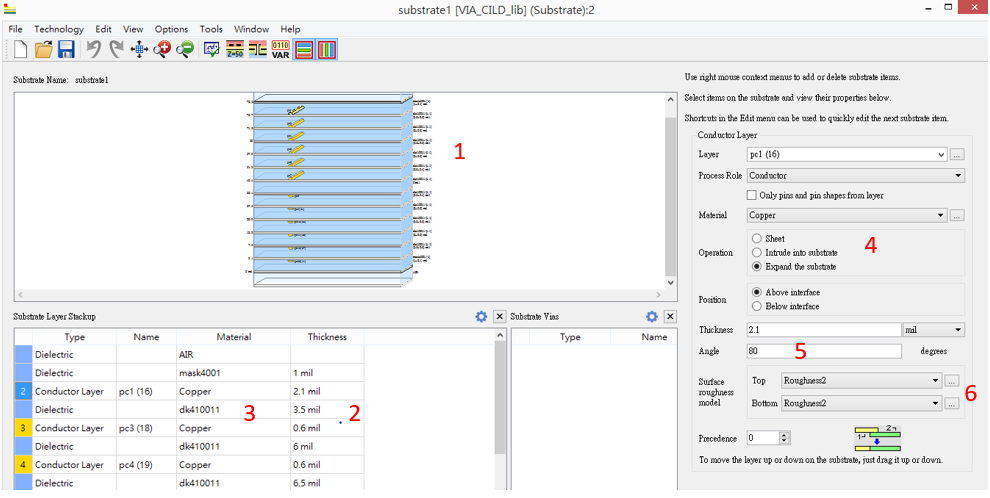
圖 2.1:Substrate interface 的主要設定區域
2.2 Adding, Moving, and Deleting Layers
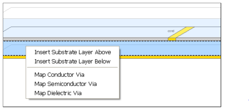
Substrate view 可用來檢視 stackup 並進行基本編輯。若要新增或刪除 substrate item,在 substrate view 中按滑鼠右鍵,從 pop-up menu 選擇對應操作。
2.3 Dielectric layer material Dk/Df
在 Dielectrics material table 中設定:
Real= Dk。TanD= Df。
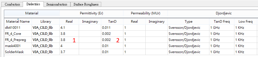
圖 2.3:Dielectric material 的 `Real (Dk)` 與 `TanD (Df)`
2.4 Calculate impedance
CILD 可用來分析 transmission line 的 physical parameter、substrate thickness 與 material parameter,藉此得到所需的 characteristic impedance。CILD analysis 產生的 parameter 可轉移到 ADS 作為 Technology Line Type,並可在 pre-layout schematic 中使用。
操作流程:
- 設定 layer combination。
- 設定 geometry 與 frequency。
- 在右下角查看 electrical result。
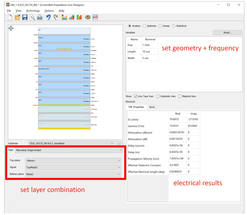
圖 2.4:Layer combination、geometry / frequency 與 electrical results
2.5 Optimize
若要針對 target impedance 尋找所需 trace width,可切換至 Optimize,再使用 Width 旁的 Optimize 讓 CILD 計算對應值。
- 選擇
Optimize。 - 設定 target impedance
Zc。 - 在
Width旁按Optimize。 - 在右下角查看 electrical result。
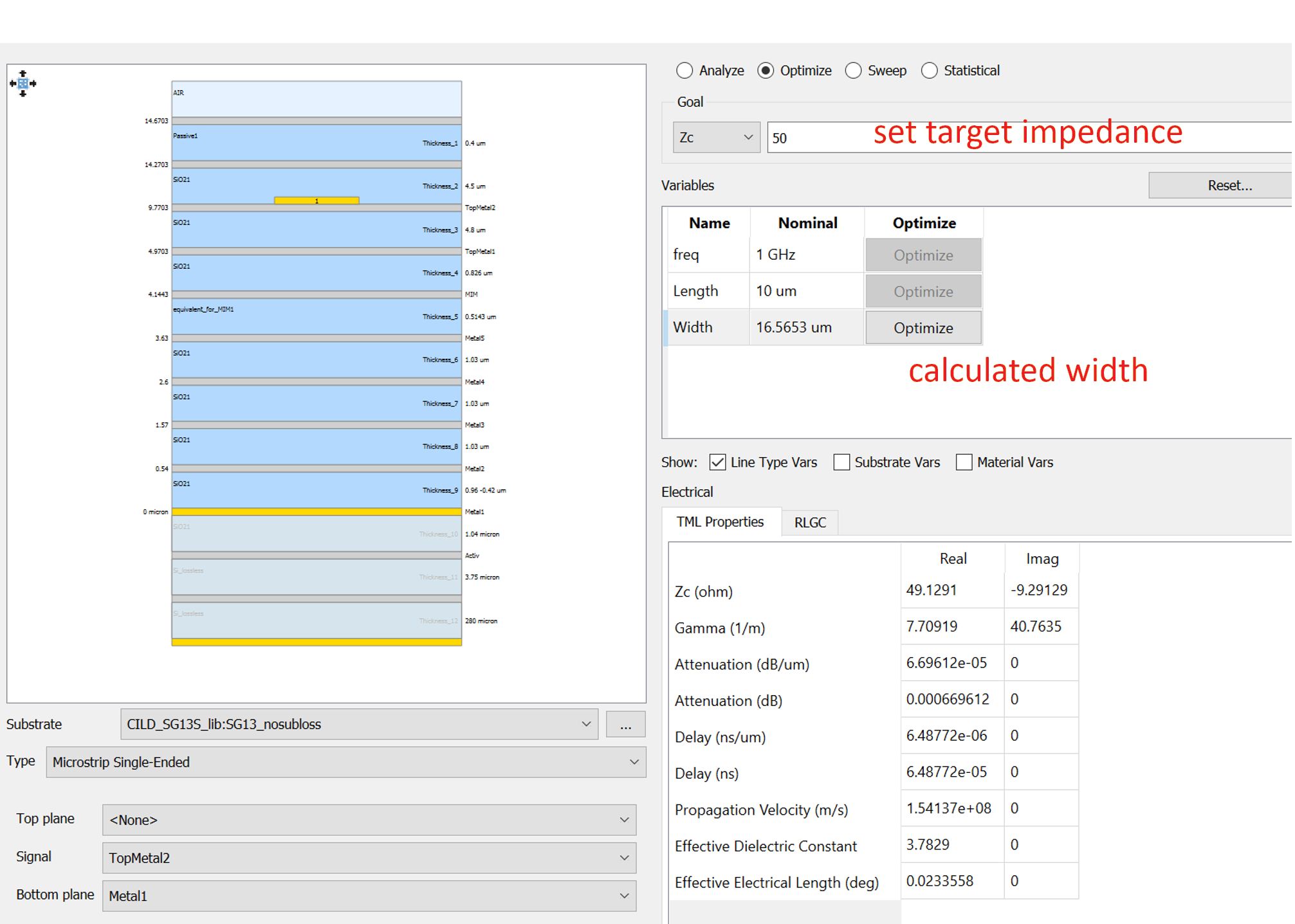
圖 2.5:Target impedance 與 calculated width 範例