第 1 章 - Basic Simulation Template
來源 PDF 頁碼: 6–14
目錄
- Stackup reference
- 1.1 Open file
- 1.2 Set stackup
- 1.3 Simulation
- 1.4 Optimize
- 1.5 Sweep
- 1.6 W-element Extraction
Stackup reference
來源章節開頭提供以下 stackup reference。此表格包含 layer、thickness、glass style、hybrid material、Dk / Df 等多層關係,因此保留為原始圖像,避免破壞 merged-cell 與欄位關係。
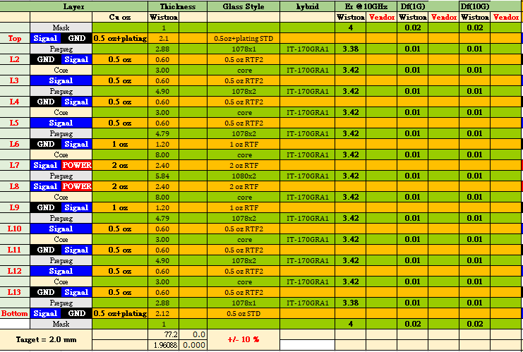
Chapter 1:stackup reference
1.1 Open file
- 在 desktop 雙擊
Advanced Design System。

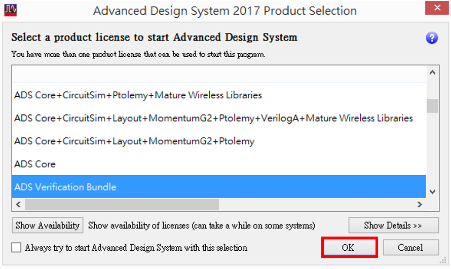
- 在 product selection 視窗選擇可用的 product license,然後按
OK。
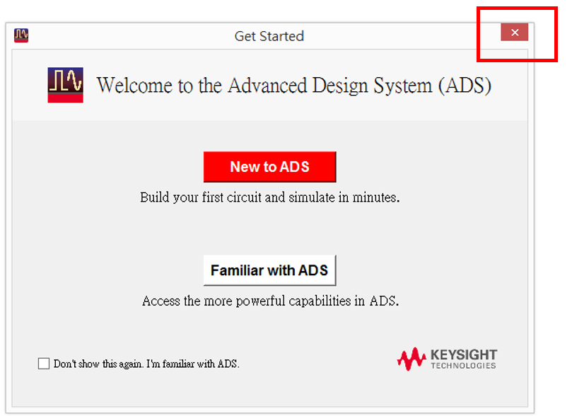
- 關閉
Get Started視窗。
- 按工具列的 Workspace 圖示,開啟 workspace。
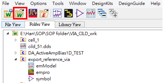
- 開啟
SOP folder。
- 開啟
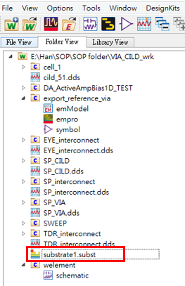
VIA_CILD_wrk。

- 在 workspace 中開啟
substrate1.subst。
1.2 Set stackup
- 依 stackup 設定各 layer thickness。
- 將 conductor layer 的
Angle設為80 degrees。 - 在
Operation選擇Expand the substrate。 - 在
Position選擇Below interface。
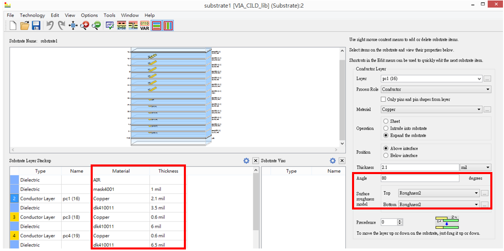
圖 1.8:Substrate stackup 與 conductor layer 設定
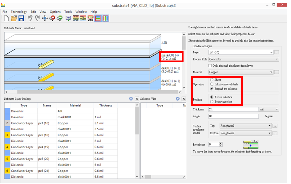
圖 1.9:`Operation`、`Position` 與 surface roughness model 設定
- 開啟
Surface Roughnessmaterial library,選擇Hammerstadmodel,並使用2 umroughness。
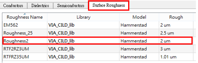
圖 1.10:`Roughness2` 使用 `Hammerstad` model,roughness 為 `2 um`
- 開啟
Dielectrics,依來源設定 material parameter:
| Material | Real (Dk) | TanD (Df) |
|---|---|---|
mask4001 |
4 | 0.01 |
dk410011 |
4.1 | 0.011 |
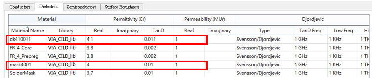
圖 1.11:Dielectric material 的 Dk / Df 設定
1.3 Simulation
- 按工具列的
Controlled Impedance Line圖示。

- 選擇
Analyze。 - 設定以下參數:
| Parameter | Value |
|---|---|
Freq |
10 GHz |
Width |
4.8 mil |
- 按執行圖示開始計算。
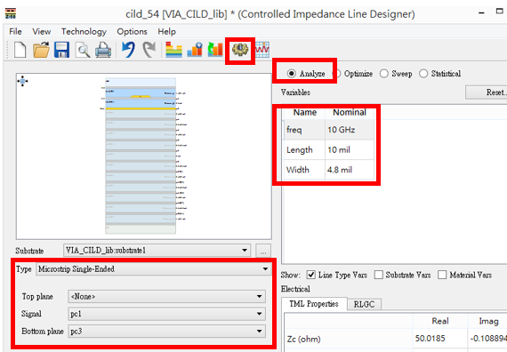
圖 1.13:Controlled Impedance Line 的 Analyze 設定
1.4 Optimize
- 選擇
Optimize。 - 將 target impedance
Zc設為40。 - 在
Width變數旁選擇Optimize。 - 按執行圖示開始計算。
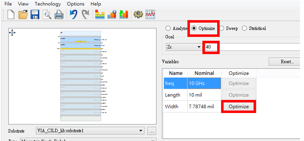
圖 1.14:以 `Zc = 40` Optimize `Width`
1.5 Sweep
- 選擇
Sweep。 - 勾選
Material Vars。 - 對
Width設定 sweep range:
| Parameter | Value |
|---|---|
Start |
7 mil |
Stop |
10 mil |
Step |
1 mil |
Npts |
4 |
- 按執行圖示開始 sweep。
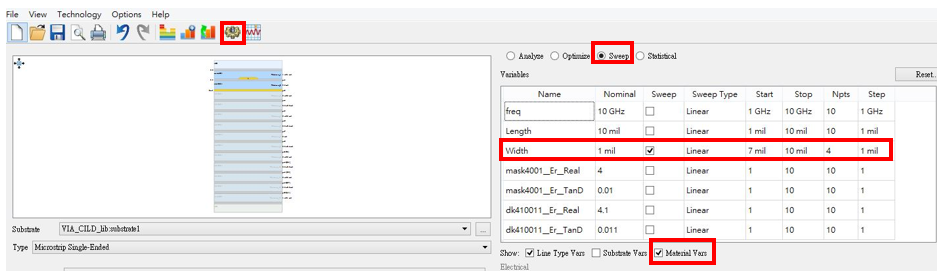
圖 1.15:`Width` sweep 設定
1.6 W-element Extraction
- 在 ADS schematic 右側元件視窗選擇
TLines-Line Type。
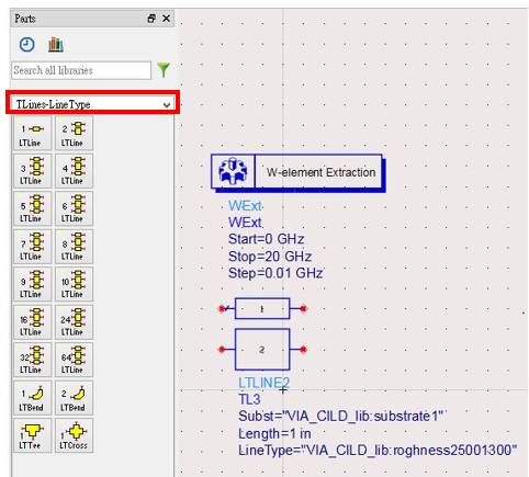
W-element Extraction 與 `TLines-Line Type` 元件畫面
來源畫面中的 Line Type 設定包含:
| Field | Source value |
|---|---|
Line Type |
VIA_CILD_lib:R2dk0014 |
Length |
1 in |
Substrate |
VIA_CILD_lib:substrate1 |
ReuseRLGC |
NO |
W_FileFormat |
HSPICE subckt with tabular RLGC data |
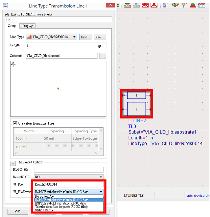
W-element / Line Type 的 `Advanced Options` 畫面