Stackup 與 Via 設定
4. Setup Stackup
- Workflow sidebar → 選擇
Check Stackup。 Enforce Causality→ 勾選。View Material。
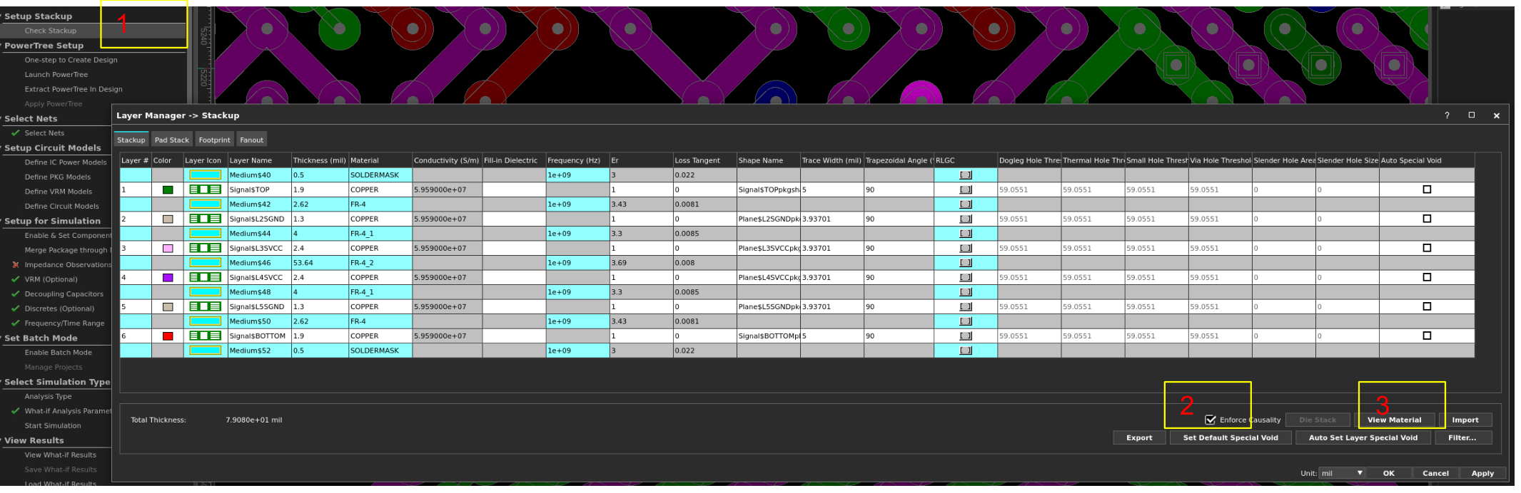
5. Setup Stackup
- 選擇
D-Sarkar Model。 - 新增 Material(Solder Mask 與 Stackup Material)。
- 設定:
- Frequency:
1000 MHz - Er:Stackup 的平均值
3.3 - Df:
1 GHz的平均值0.008
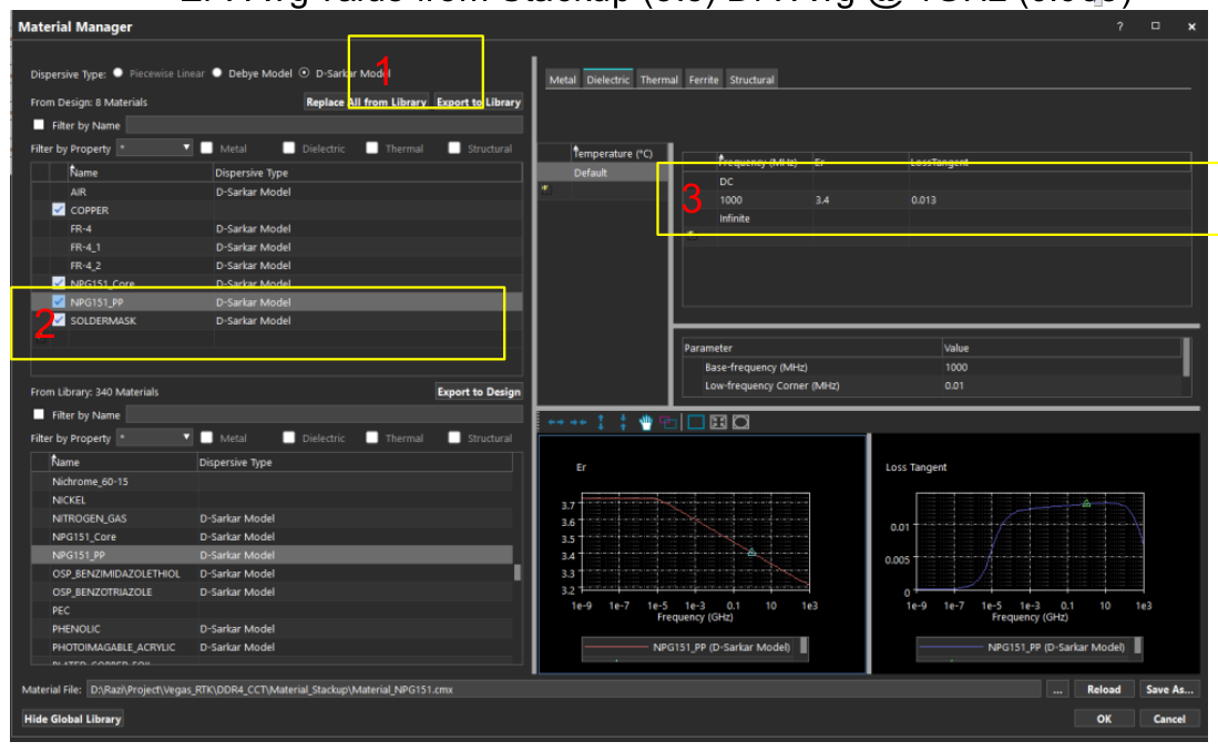
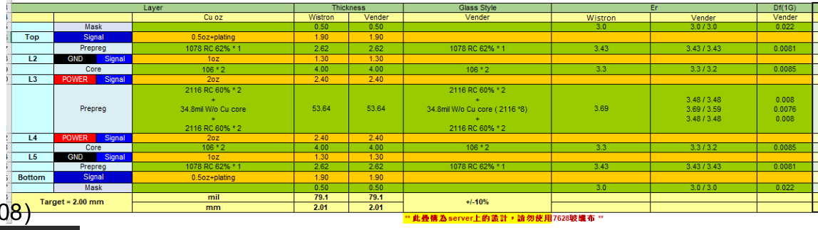
Note:較建議先將 material 加入 global library,再 export 到 project library。Simulation 有時會因找不到 material definition 而產生 error。
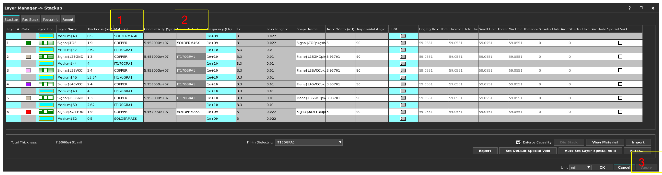
6. Setup Stackup
- 修改
Materialcolumn。 - 修改
Fill-in Dielectriccolumn。 Apply→OK。
PI-AC simulation 可忽略其他項目。
7. Modify the Via DHS = FHS + 2 (mil)
- 從 Stackup 切換到
Pad Stack。 - 選擇名稱以
[V]開頭的 via。 - 將 outer Diameter 從 FHS 修改為 DHS。
Apply→OK。
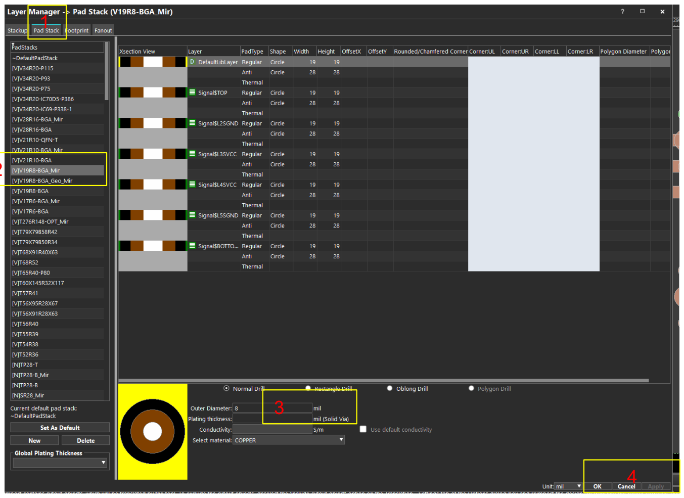
Note: 1. 以
[N]開頭的 Padstack 未使用於 board files,可忽略。 2. 以[V]開頭的 Padstack 有使用於 board files,因此需要修改 FHS → DHS value。 3.V19R8via 的Outer Diameter由8修改為10。