第 2 章-Post-layout 模擬
來源 PDF 頁碼: 23–55
目錄
- 2.1 匯入檔案
- 2.2 將檔案匯入 PinToPinSetup
- 2.3 開啟檔案
- 2.4 設定 stackup
- 2.4.1 材料
- 2.4.2 Roughness
- 2.4.3 Etch
- 2.5 設定 Via 與 GND
- 2.6 設定 hole diameter、padstack、pad 與 anti-pad
- 2.7 設定模擬範圍
- 2.8 設定 PWR
- 2.9 整理 structure
- 2.10 設定 HFSS Extents
- 2.11 設定 mesh
- 2.12 HFSS 模擬
- 2.13 SIwave
- 2.13.1 將 trace type 改為 line
- 2.13.2 設定模擬範圍
- 2.14 Circuit
- 2.14.1 開啟 Circuit
- 2.14.2 開啟 Component Libraries
- 2.14.3 Circuit connection
- 2.14.4 TDR circuit connection
- 2.14.5 Channel loss
- 2.14.6 Via simulation
- 2.14.7 Trace simulation
- 2.14.8 Channel-loss simulation
- 2.15 檔案輸出
2.1 匯入檔案
- 開啟 Computer。
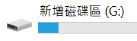
- 開啟
Local Disk (G:)。
- 建立個人資料夾。
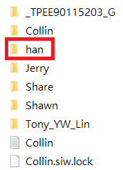
- 將要模擬的 board files 複製到個人資料夾。
2.2 將檔案匯入 PinToPinSetup
- 開啟
C:\Program Files\AnsysEM\AnsysEM21.2\Win64。

- 雙擊
PinToPinSetup。

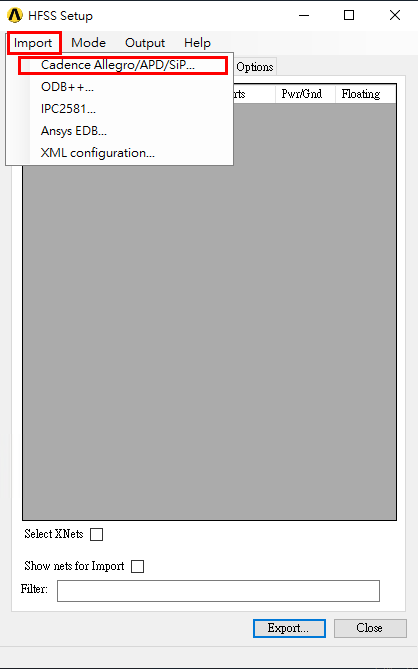
- 將
.brd檔匯入 HFSS Setup(PinToPinSetup)。
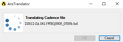
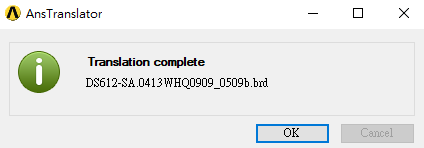
- 選擇要模擬的 net。
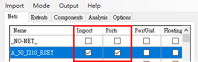
圖 2.9:選擇 net
- 選擇 reference GND/POWER nets。
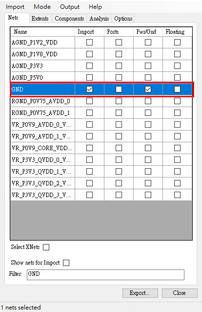
圖 2.10:選擇 reference GND
- 在
Extents下,將Factor/Distance設為0.05-0.1。
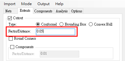
圖 2.11:設定 Factor/Distance
- 在
Components下選擇 IC name。 - 設定 component orientation:
- Chip 位於 board 上側:
Chip down - Chip 位於 board 下側:
Chip up
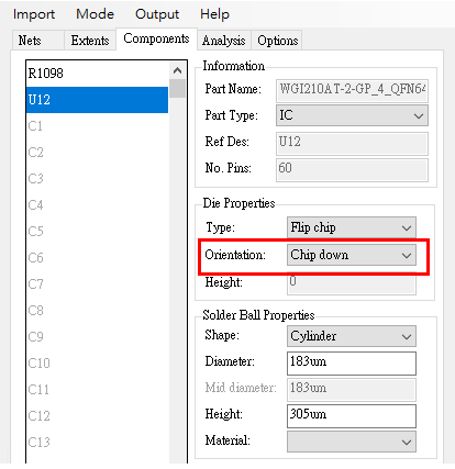
圖 2.12:設定 orientation
- 一般 solder-ball 設定使用:
| Parameter | Value |
|---|---|
Shape |
Cylinder |
Diameter |
default value |
Height |
default value |
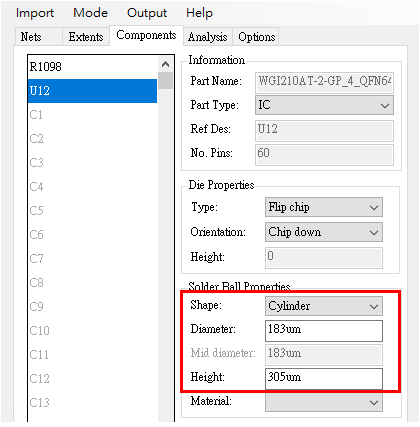
圖 2.13:設定 solder ball
- 1 mm-pitch BGA solder ball 設定:
| Parameter | Value |
|---|---|
Shape |
Spheroid |
Diameter |
400 um |
Mid Diameter |
500 um |
Height |
300 um |
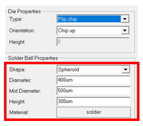
圖 2.14:1 mm-pitch BGA solder ball
- 在
Options下,從 port naming convention 移除$PINNAME。
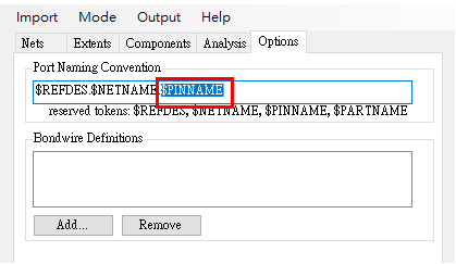
圖 2.15:刪除 $PINNAME
2.3 開啟檔案
- 開啟 Ansys Electronics Desktop。
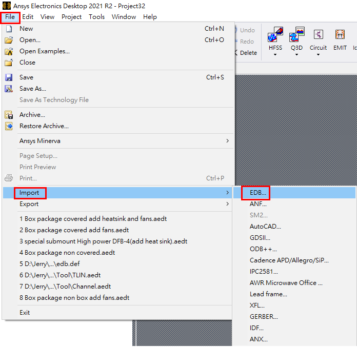
- 選擇
File>Import>EDB。
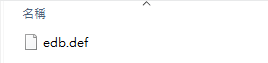
- 選擇轉換後的 EDB file。
2.4 設定 stackup
- 開啟 stackup editor
 。
。 - 在 layer table 中選擇
FR4-epoxy。
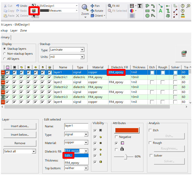
圖 2.19:設定材料的操作路徑
- 在
Dielectric fill旁選擇Edit...。 - 選擇
Add Material...。
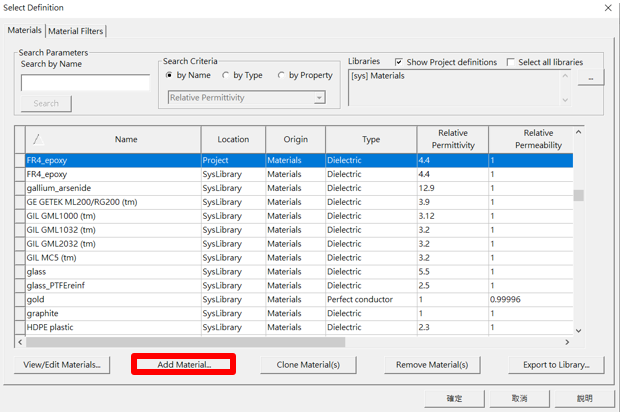
圖 2.20:建立材料
- 輸入 material name。
- 選擇
Set Frequency Dependency...。 - 選擇
Djordjevic-Sarkar Model Input。
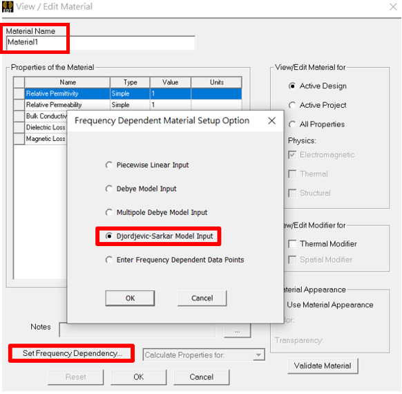
圖 2.21:設定材料 frequency dependency 的路徑
- 輸入 frequency-dependent material parameters。範例設定:
| Parameter | Value |
|---|---|
Frequency |
10 GHz |
Relative Permittivity |
2.85 |
Loss Tangent |
0.0016 |
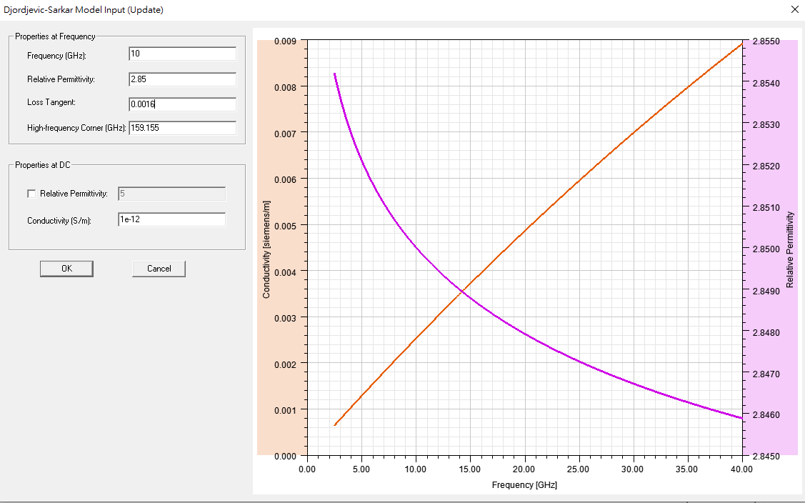
圖 2.22:設定材料 frequency parameters
2.4.1 材料
- 選擇
Select signal。 - 將 signal material 設為
copper。
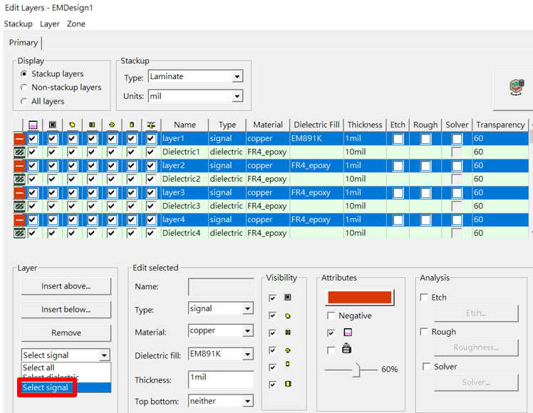
圖 2.23:選取 signal layer 的操作路徑
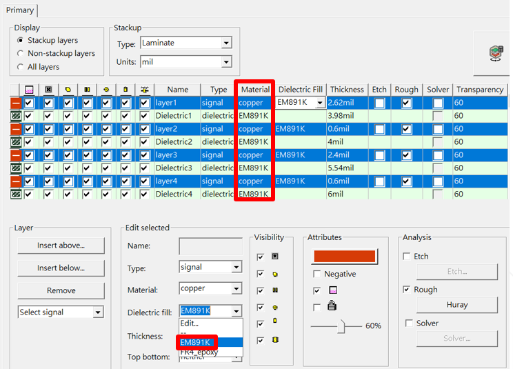
圖 2.24:設定 signal material
- 選擇
Select dielectric。
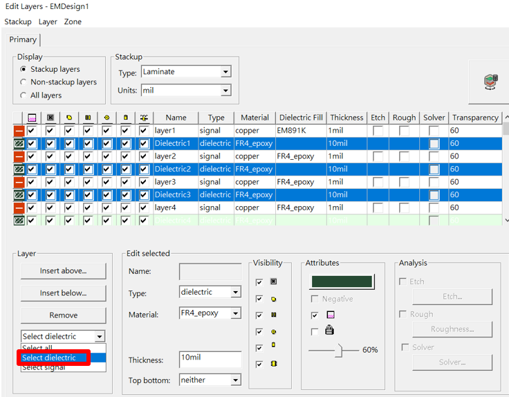
圖 2.25:選取 dielectric layer
- 將 dielectric fill 設為
EM892K。
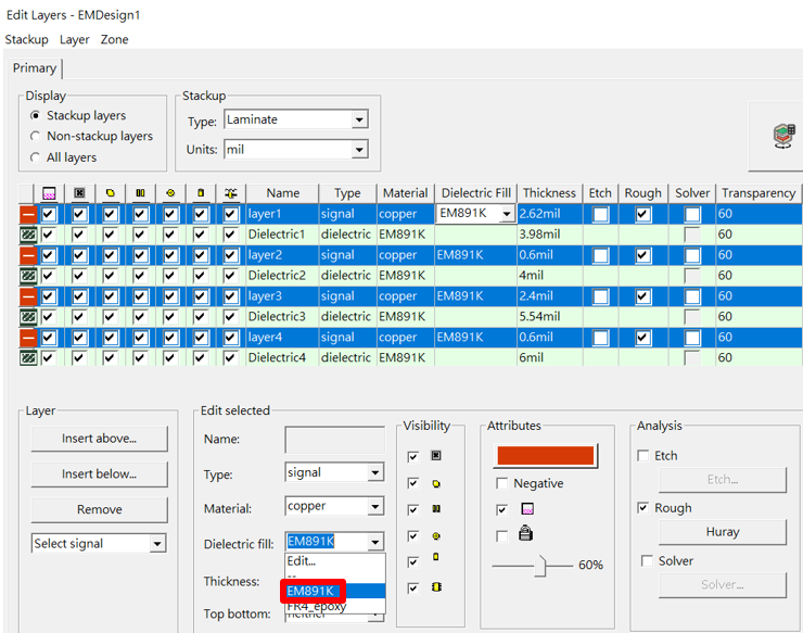
圖 2.26:設定 dielectric layer 的操作路徑
- 依 project parameters 設定 stackup thickness。
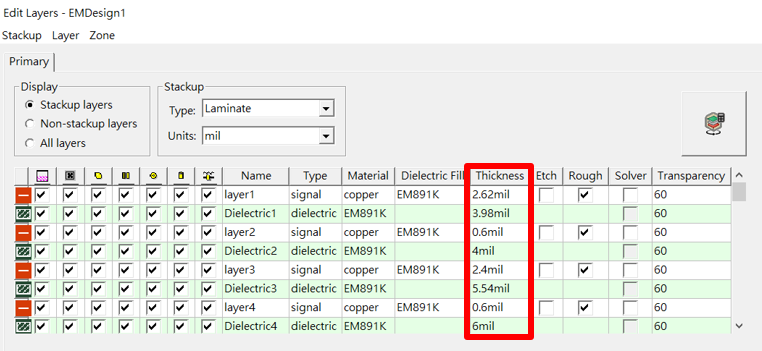
圖 2.27:設定 stackup thickness
2.4.2 Roughness
- 啟用
Roughness欄位中的 checkbox。 - 將
Nodule radius設為0.06 x Rz (um)。 - 將
Hall-Huray surface ratio設為4.9。 - 選擇
Set All Regions。
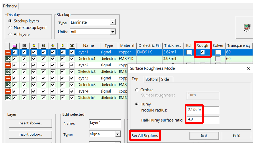
圖 2.28:設定 Roughness
Rz 參考值:
| Copper profile | Rz |
|---|---|
| HTE | 8 um |
| RTF | 3.5 um |
| RTF2 | 3 um |
| RTF3 | 2.5 um |
| VLP | 3 um |
| HVLP | 2 um |
| HVLP2 | 1.5 um |
| HVLP3 | 1 um |
2.4.3 Etch
- 啟用
Etch欄位中的 checkbox。 - 設定 top 與 bottom parameters。
- 依實際情況將
Etch Factor設為2.5或-2.5。
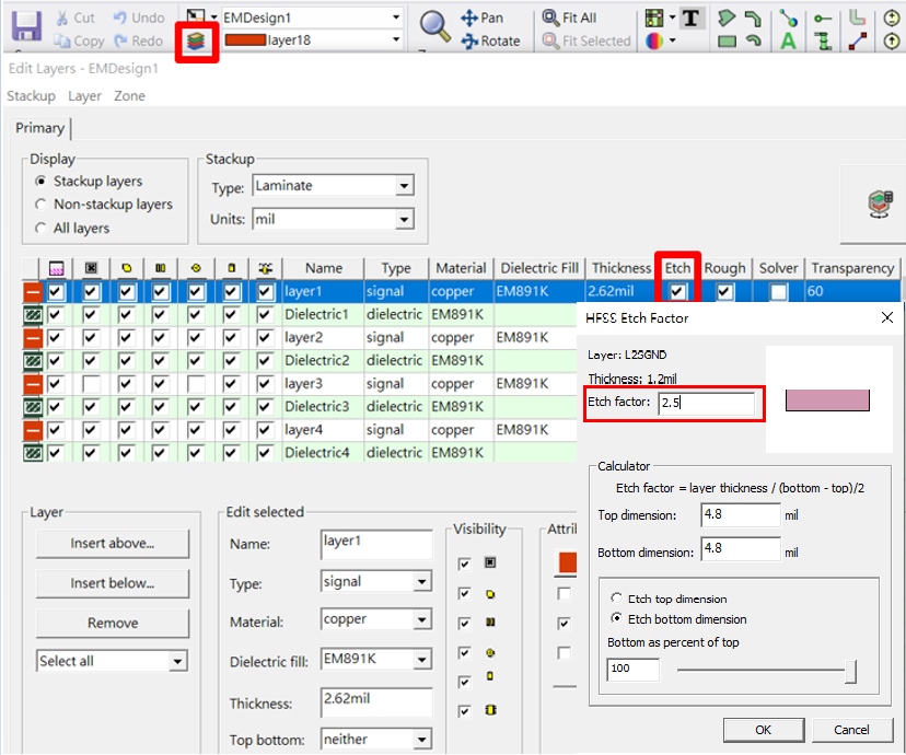
圖 2.29:設定 Etch
2.5 設定 Via 與 GND
- GND via 不要指定
Backdrill Top或Backdrill Bottom。 - 模擬前,確認 signal via 的 start/stop layer 與 Backdrill 定義。
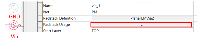
圖 2.30:設定 via
2.6 設定 hole diameter、padstack、pad 與 anti-pad
Hole Diameter比 default drill value 增加2 mil。例如:由8 mil改為10 mil。- 以手動方式或依 net name 設定 pad/anti-pad dimensions。
- 選擇 anti-pad style;通常使用 bullet-style anti-pad。
- 只有在 drill 必須偏離 padstack center 時,才使用
Offset x/y。
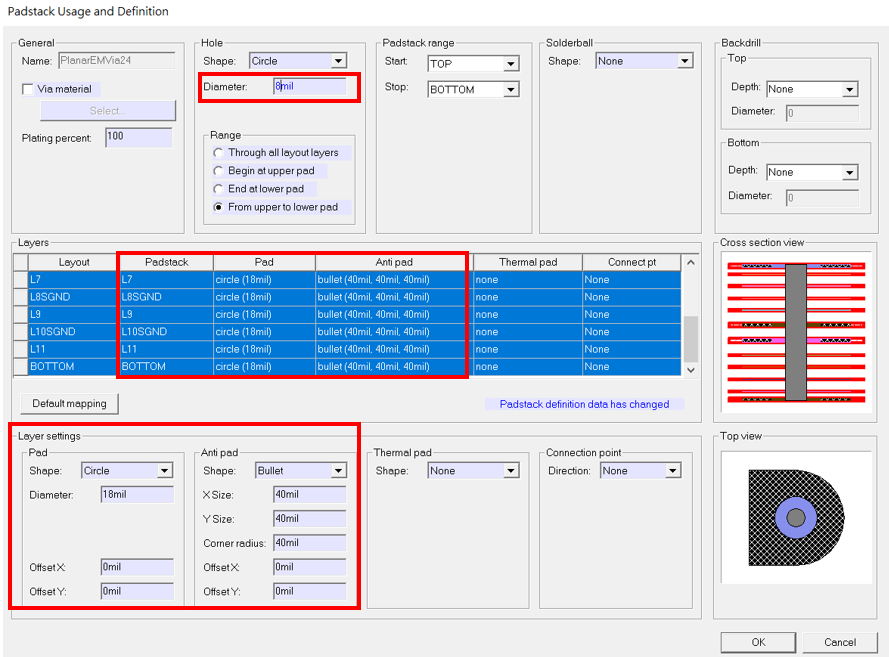
圖 2.31:設定 padstack、pad 與 anti-pad
- 設定 net name。
- 依需求設定
Backdrill Top與Backdrill Bottom。
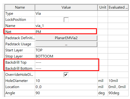
圖 2.32:設定 pad 與 anti-pad
2.7 設定模擬範圍
- 啟用 selection-window tool
 。
。 - 選取 trim area。
Cutout 規則 - 若要保留圖中的綠框區域,需選取較大的紅框區域。 - 至少包含一個相鄰的 GND structure。 - 不要將 component 從中間切斷,必須保留 component 完整性。 - Signal via 附近若有 power via,進行 via simulation 時應一併保留。
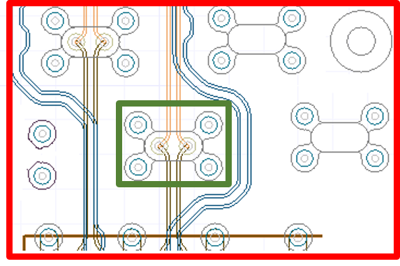
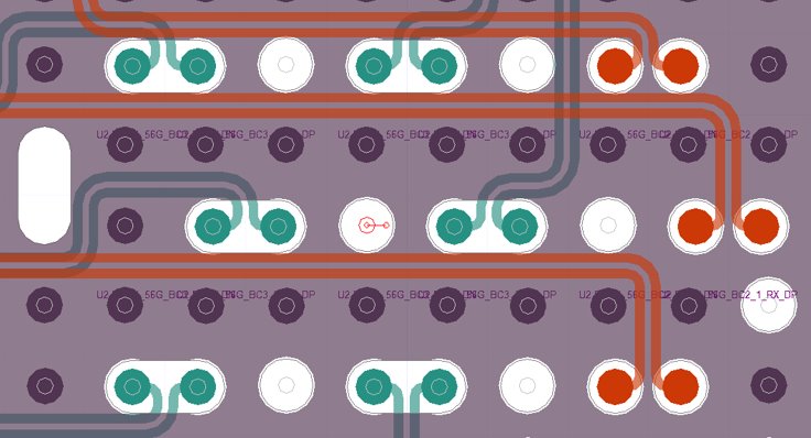
圖 2.33:選取 trim area
- 選擇
Cutout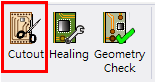 。
。 - 選擇要保留的 nets。
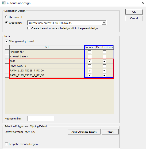
圖 2.34:選擇要保留的 net
- 選擇
Create new,避免覆寫 original file。 - 選擇
Auto Generate Extent,並將Expansion設為0。
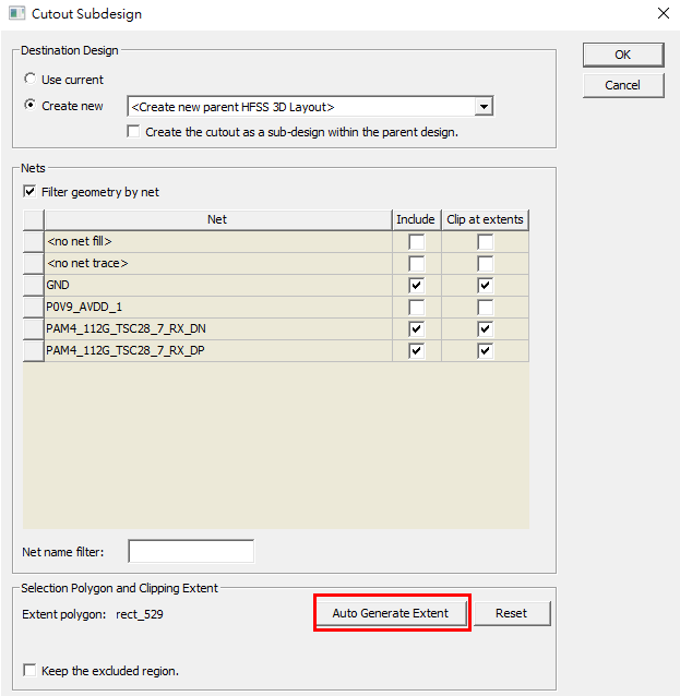
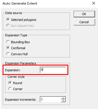
圖 2.35:設定 Expansion
2.8 設定 PWR
模擬範圍包含 power structure 時,需指定 capacitor model。設定值如下:
| Parameter | Value |
|---|---|
R |
10m |
L |
400p |
C |
10uF |
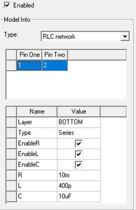
圖 2.36:設定 PWR
正式使用前,需確認上述設定的 SI units 與 component model 定義。
2.9 整理 structure
完成 Cutout 後,移除操作過程產生的非預期 polygon。
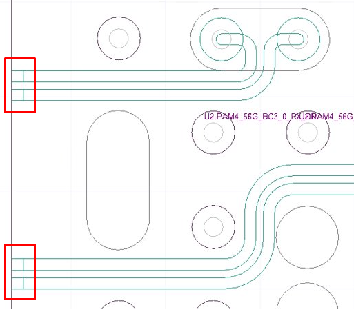
2.10 設定 HFSS Extents
- 選擇
HFSS Extents。 - 選擇
Edit。
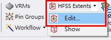
圖 2.38:編輯 HFSS Extents
- 將
Horizontal設為0。 - 將
Positive padding設為0.1。
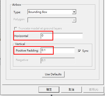
圖 2.39:設定 Airbox Bounding Box
2.11 設定 mesh
- 選擇
HFSS 3D Layout。 - 選擇
Design Settings...。 - 開啟
HFSS Meshing Method。 - 選擇
Phi plus [Beta]。 - 取消
Use alternative mesh methods as fallback。
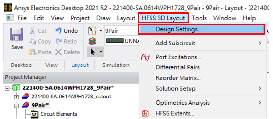
圖 2.40:Mesh 設定路徑
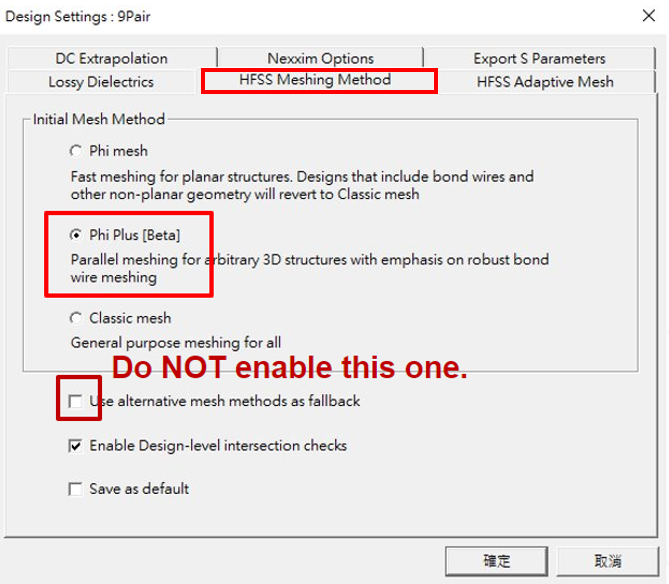
圖 2.41:Mesh 設定視窗
2.12 HFSS 模擬
- 在
Analyze上按右鍵。 - 選擇
Add HFSS Solution Setup...>Advanced。

圖 2.42:設定 solution
- 選擇
Multi-Frequencies。 - 新增 adaptive frequencies:
0.1 GHz、30 GHz、60 GHz。 - 將
Maximum Number of Passes設為999。
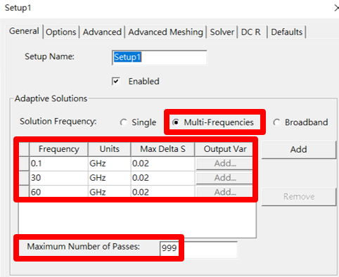
圖 2.43:設定 frequency
- 在
Options下,將Minimum Converged Passes設為2。
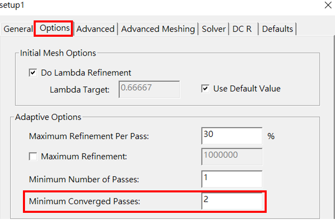
圖 2.44:設定 Minimum Converged Passes
- 在
Advanced下,將Number of sides設為8。
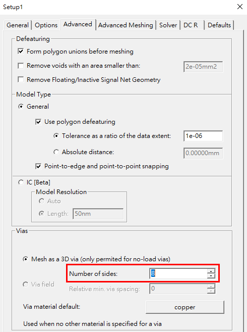
圖 2.45:設定 Number of sides
- 將 frequency sweep 設為
0 GHz至60 GHz。
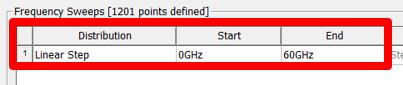
圖 2.46:設定 frequency sweep
- 選擇
Interpolation。 - 將
Max Solutions設為1000。 - 將
Error Tolerance設為0.01。
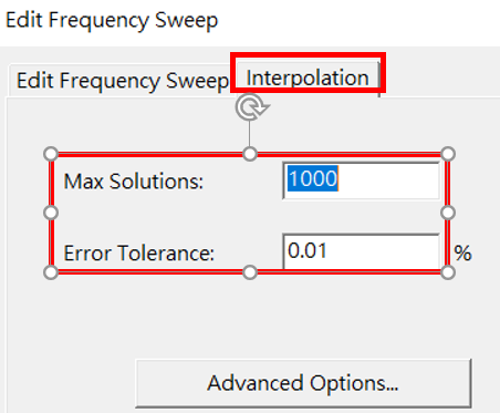
圖 2.47:設定 Interpolation
2.13 SIwave
2.13.1 將 trace type 改為 line
- 選擇一條 trace。若其 type 為
poly,需將 plane 轉換為 line。
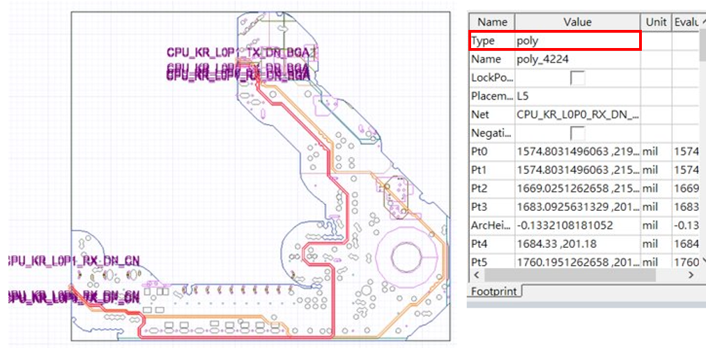
圖 2.48:Trace type 為 poly
- 選擇
Layout>Convert>Planes to Traces Options...。

圖 2.49:Planes-to-Traces Options 操作路徑
- 啟用
Allow traces with square ends。
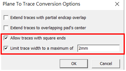
圖 2.50:設定 Planes-to-Traces Options
- 選取 trace,並執行
Planes to Traces。
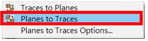
圖 2.51:將 poly 轉為 line
2.13.2 設定模擬範圍
- 新增 SIwave solution setup。
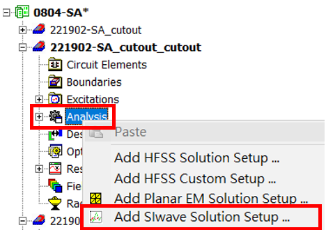
圖 2.52:新增 SIwave solution setup
- 在
General下,將 SI Simulation 設為Optimum accuracy。 - 選擇
Custom以設定 advanced options。
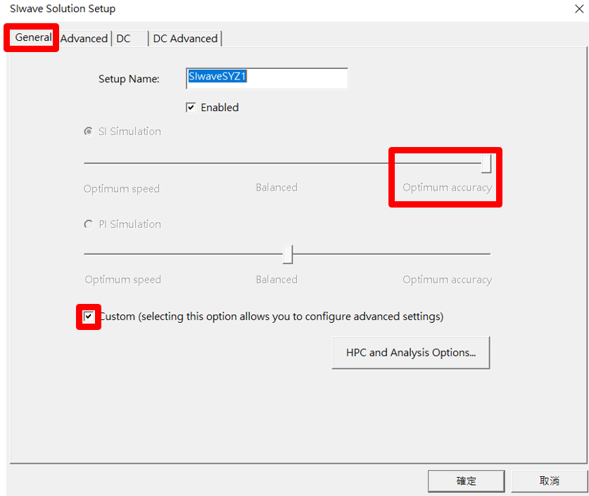
圖 2.53:SIwave custom setup
- 在
Advanced下: - 將
Do not mesh voids less than設為0。 - 將
Cross-talk threshold設為-60 dB。 - 設定 frequency range。
- 將 points 數量設為
1001。
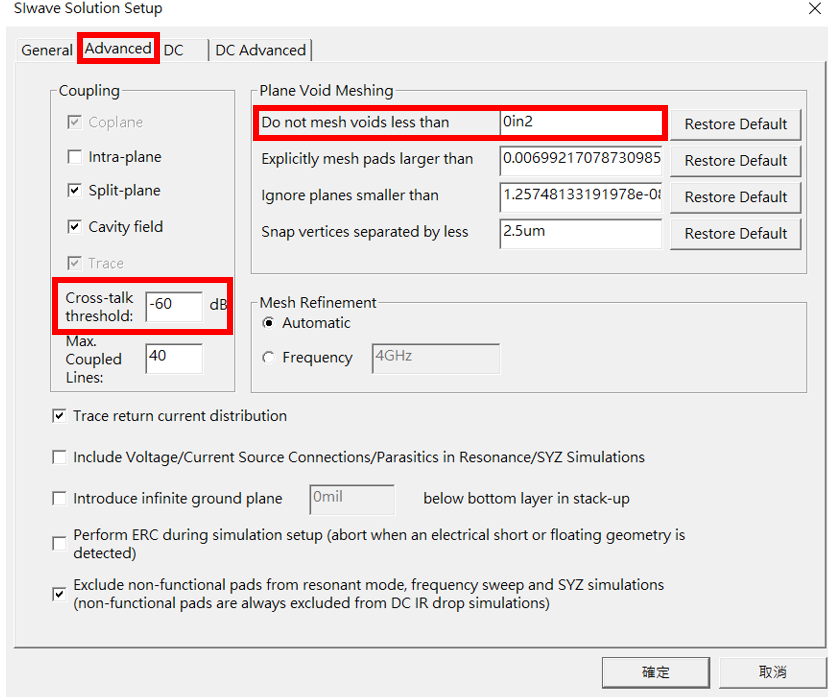
圖 2.54:設定 SIwave solution setup
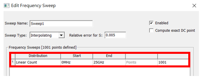
圖 2.55:設定 SIwave frequency sweep
2.14 Circuit
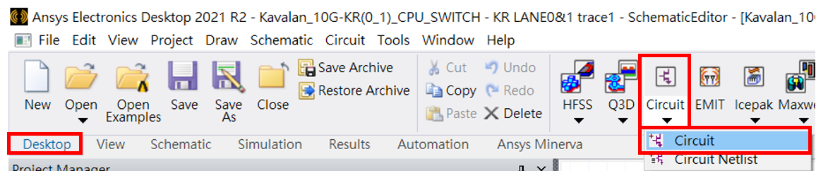
2.14.1 開啟 Circuit
- 選擇
Desktop>Circuit>Circuit。
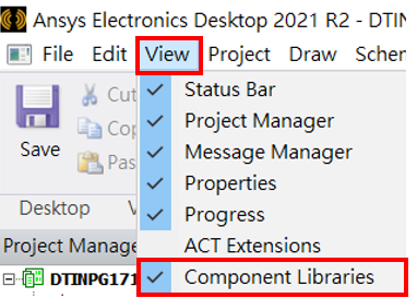
2.14.2 開啟 Component Libraries
- 選擇
View>Component Libraries。
2.14.3 Circuit connection
- 選擇
Components。 - 選擇
Nexxim Circuit Elements。
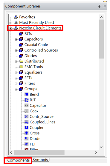
圖 2.58:Nexxim Circuit Elements
- 選擇
Group>Resistor。 - 選擇
Probes>TDR Differential_Ended: Differential Ended TDR。
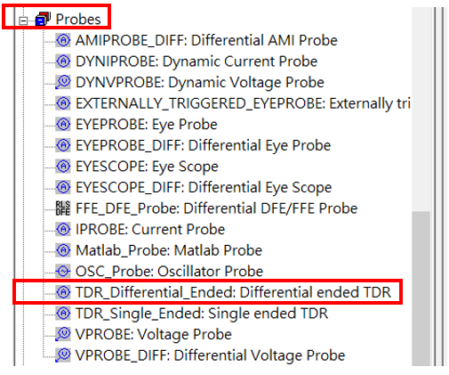
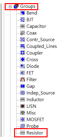
圖 2.59:Component 選取方式
2.14.4 TDR circuit connection
- 雙擊 resistor,並將 resistance 設為
50 ohm。 - 雙擊 TDR component。
- 依 rise-time reference 設定 TDR rise time。
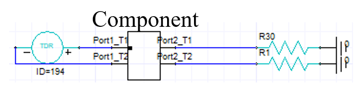
圖 2.60:TDR circuit
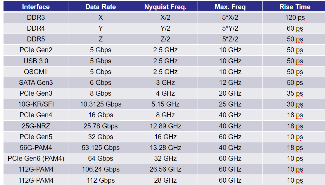
圖 2.61:TDR rise-time parameter
2.14.5 Channel loss
依下圖連接 Channel-loss circuit。
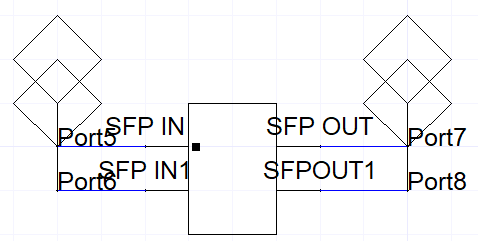
圖 2.62:Channel-loss circuit
2.14.6 Via simulation
- 在
Analysis上按右鍵,選擇Add Nexxim Solution Setup...>Transient Analysis。
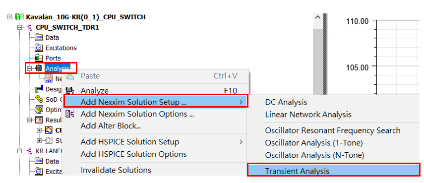
圖 2.63:Via simulation setup
- 在
Analysis Control下設定: Step:0.9 psStop:1.5 ns
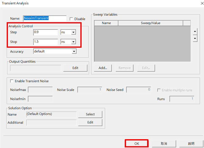
圖 2.64:Via simulation analysis control
2.14.7 Trace simulation
- 在
Analysis上按右鍵,選擇Add Nexxim Solution Options...。
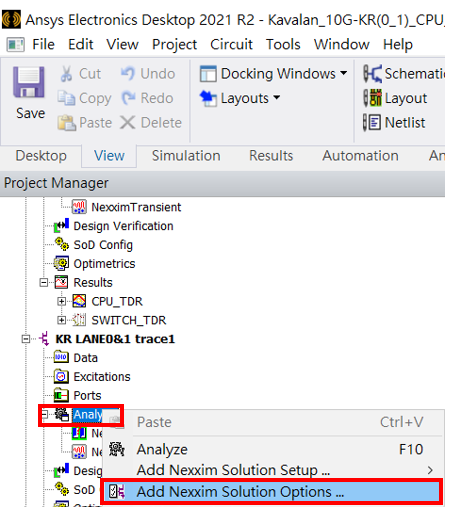
圖 2.65:Trace simulation 操作路徑
- 依下圖設定 solution options。
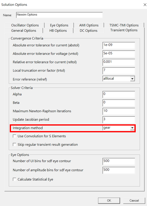
圖 2.66:Trace simulation options
- 在
Analysis上按右鍵,選擇Add Nexxim Solution Setup...>Transient Analysis。
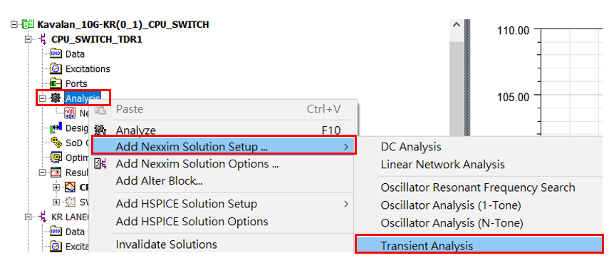
圖 2.67:Trace transient setup
- 在
Analysis Control下設定: Step:0.9 psStop:1.5 ns
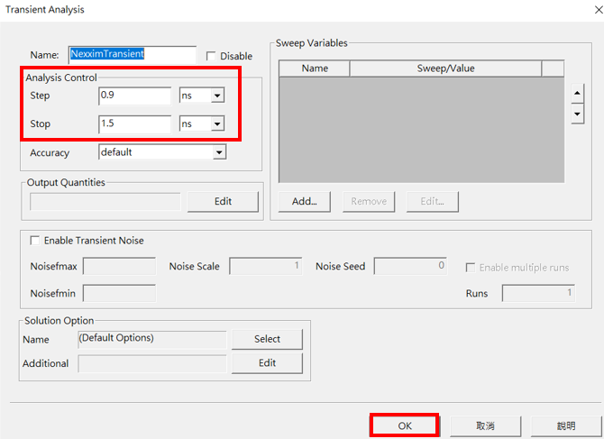
圖 2.68:Transient analysis control
2.14.8 Channel-loss simulation
- 在
Analysis上按右鍵,選擇Add Nexxim Solution Setup...>Linear Network Analysis。
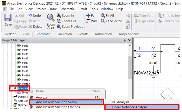
圖 2.69:Channel-loss simulation 操作路徑
- 選擇
Add。 - 依需求設定 frequency range。
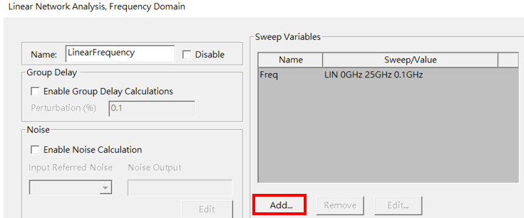
圖 2.70:Channel-loss frequency
2.15 檔案輸出
- 選擇
File>Archive...。 - 將 simulation project archive 後,上傳至核准的內部 storage location。
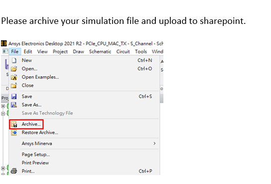
圖 2.71:檔案輸出