Diodes Buying ElevATE Is a Small Deal With a Bigger Message: AI Is Repricing Semiconductor Test
Diodes Buying ElevATE Is a Small Deal With a Bigger Message: AI Is Repricing Semiconductor Test
- Source: SemiVision
- Author: SEMIVISION
- Published: 2026-08-28T10:08:26+08:00
- URL: https://tspasemiconductor.substack.com/p/diodes-buying-elevate-is-a-small
中文翻譯與英文原文(雙語)
(2) Diodes 收購 ElevATE 雖是小交易,卻傳遞重要訊息:AI 正在重新定價半導體測試 --- (2) Diodes Buying ElevATE Is a Small Deal With a Bigger Message: AI Is Repricing Semiconductor Test


Diodes Buying ElevATE Is a Small Deal With a Bigger Message: AI Is Repricing Semiconductor Test
Diodes 收購 ElevATE 雖為小型交易,卻傳遞重大訊息:AI 正在重新定價半導體測試
Original Article By SemiVision Research [Reading time: 10 mins]
原文作者:SemiVision Research [閱讀時間:10 分鐘]

Aug 28, 2026
∙ Paid∙ 付費
Share分享
Diodes Buying ElevATE Is a Small Deal With a Bigger Message: AI Is Repricing Semiconductor Test
Diodes 收購 ElevATE:一筆小交易背後的重大訊息——AI 正在重新定義半導體測試的價值
Diodes’ US$250 million all-cash acquisition of ElevATE Semiconductor is easy to overlook.
Diodes 以 2.5 億美元全現金收購 ElevATE Semiconductor 的交易,很容易被忽視。
Diodes Incorporated Completes Acquisition of ElevATE Semiconductor
Diodes Incorporated 完成對 ElevATE Semiconductor 的收購
It should not be.但事實不該如此。
The transaction is small relative to the tens of billions of dollars being deployed into leading-edge fabs, HBM capacity, advanced packaging, and AI accelerators. But strategically, it captures one of the more important shifts happening in the semiconductor value chain:
相較於投入先進晶圓廠、HBM 產能、先進封裝與 AI 加速器的數百億美元資金,此筆交易規模確實不大。然而從策略層面來看,它捕捉到了半導體價值鏈中正在發生的關鍵轉變之一:
As compute systems become more heterogeneous, expensive, and difficult to assemble, test intensity is rising faster than unit volume.
隨著運算系統變得更加異質、昂貴且組裝困難,測試強度正以快於出貨量的速度攀升。
That distinction matters.
這一區別至關重要。
AI is not simply creating more semiconductor demand. It is increasing the number of electrical, thermal, structural, and functional verification steps required per device.
人工智慧並非僅僅創造更多的半導體需求,而是增加了每個裝置所需的電氣、熱力、結構與功能驗證步驟數量。
This is moving semiconductor test from a relatively mature back-end function into a higher-value infrastructure layer.
這正將半導體測試從相對成熟的後端功能,提升為更具價值的基礎設施層級。
ElevATE sits directly in that transition.
ElevATE 正處於此一轉型的關鍵位置。
The company develops high-performance analog and mixed-signal ICs used inside automated test equipment, including pin electronics, parametric measurement units, and device power supplies.
該公司開發高性能類比與混合訊號 IC,用於自動測試設備(ATE)內部,包括接腳電子元件、參數測量單元及裝置電源供應器。
These are not glamorous products.
這些產品雖不引人注目,
But they are increasingly important because the economics of modern ATE are shifting toward:
但其重要性日益提升,因為現代 ATE 的經濟模式正朝向以下方向轉變:
more channels,更多通道,
higher density,更高密度,
more parallelism,更多並行性,
tighter power control,更嚴格的電源控制,
more precise measurements,
更精確的測量,
and lower test cost per device.
並降低每顆裝置的測試成本。
That makes ElevATE less interesting as a standalone analog IC vendor than as a supplier into the growing test-content-per-chip equation.
這使得 ElevATE 作為一家獨立的類比 IC 供應商吸引力較低,但作為日益增長的「每晶片測試含量」方程式中的供應商則更具價值。

7月27日7 月 27 日
Below we will share:以下我們將分享:
AI Has Changed the Economics of Test
AI 已改變測試的經濟效益
Test Is Becoming a Yield-Protecting Layer
測試正成為保護良率的關鍵層級
ATE Is Already Showing AI-Driven Operating Leverage
ATE 已展現 AI 驅動的營運槓桿
The Next Shift: From Standalone Test to Integrated Test
下一波變革:從獨立測試邁向整合測試

5月25日5 月 25 日

The Semiconductor Wafer Test Asia Conference (SWTest Asia) is celebrating over 5 years as the only industry event that focuses on all the aspects associated with microelectronic wafer and die level testing within the Asia test community. The conference has the perfect mixture of manufacturer and vendor presentations. It is a probe technology forum where attendees come to learn about recent developments in the industry and exchange ideas. There is a relaxed atmosphere with a golf tournament, an EXPO, social activities and plenty of time for informal discussion and networking.
半導體晶圓測試亞洲會議(SWTest Asia)已邁入第五個年頭,是亞洲測試社群中唯一專注於微電子晶圓與晶粒層級測試各方面之產業盛會。本會議完美結合了製造商與供應商的專題演講,成為探針技術的交流平台,讓與會者得以了解產業最新發展並交換意見。會議氛圍輕鬆愜意,除高爾夫球錦標賽、博覽會及各項社交活動外,更提供充裕時間供與會者進行非正式討論與人脈交流。
AI Has Changed the Economics of Test
人工智慧已改變測試的經濟結構
The traditional semiconductor test model was relatively straightforward.
傳統的半導體測試模式相對單純直接。
A monolithic chip moved through wafer sort, packaging, final test, and perhaps reliability screening.
單一晶片依序通過晶圓分選、封裝、最終測試,並可能進行可靠性篩選。
The cost structure was manageable because the device architecture itself was relatively contained.
成本結構之所以可控,是因為該元件架構本身相對封閉。
AI accelerators are different.
AI 加速器則截然不同。
A modern high-end AI package can combine:
現代高階 AI 封裝可能整合:
a large compute die,一顆大型運算晶粒,
multiple HBM stacks,多個 HBM 堆疊,
I/O dies,I/O 晶片,
chiplets,小晶片(chiplets),
SerDes,SerDes,
interposers,中介層,
RDL,重佈線層(RDL),
advanced power delivery,先進電源傳輸,
and increasingly complex substrate interfaces.
以及日益複雜的基板介面。
In future architectures, optical I/O and co-packaged optical engines may be added to the same system.
在未來的架構中,光學 I/O 與共封裝光學引擎可能會被整合至同一系統。
This changes the test problem from:
這將測試問題從:
Is the chip functional?晶片是否正常運作?
to:致:
Is every component functional, are all interfaces within spec, and does the integrated system still behave correctly after assembly?
轉變為: 每個元件是否正常運作、所有介面是否符合規格,以及整合系統在完成組裝後是否仍能正確運作?
That is a materially more difficult problem.
這是一個實質上更為困難的問題。
And more importantly, it creates more test insertions.
更重要的是,它會產生更多的測試插入點。
A complex AI package may require verification across:
複雜的 AI 封裝可能需要進行以下驗證:
Wafer Sort晶圓測試
→ Pre-Bond Test→ 預鍵結測試
→ Known-Good-Die Screening
→ 已知良品晶粒篩選
→ HBM Stack Test→ HBM 堆疊測試
→ Chiplet Interconnect Test
→ 小晶片互連測試
→ Package Test→ 封裝測試
→ System-Level Test→ 系統層級測試
→ Reliability / Burn-In→ 可靠性 / 老化測試
The total number of units shipped does not need to increase dramatically for test demand to rise.
出貨總量無需大幅成長,測試需求即可提升。
This is whytest intensityis becoming the better metric.
這正是測試強度成為更關鍵指標的原因。
HBM Is the Clearest Example of Why Test Must Move Earlier
HBM 是最明確的例證,說明為何測試必須提前進行。
HBM makes the economics obvious.
HBM 讓相關經濟效益顯而易見。
Suppose one DRAM die inside a stack has a latent defect.
假設堆疊中的一顆 DRAM 晶粒存在潛在缺陷。
If the defect is identified early, the loss is limited.
若能及早發現缺陷,損失便可控制在有限範圍內。
If the defect is identified only after multiple dies are stacked, bonded, packaged next to an expensive GPU, and integrated into a high-value package, the economic loss becomes much larger.
若缺陷僅在多個晶粒堆疊、接合、封裝於昂貴的 GPU 旁,並整合至高價值封裝後才被發現,所造成的經濟損失將大幅擴大。
This is why the industry is moving toward a hierarchy of:
這正是產業朝向以下層級架構發展的原因:
Known Good Die → Known Good Stack → Known Good Package
已知良好晶粒(Known Good Die)→ 已知良好堆疊(Known Good Stack)→ 已知良好封裝(Known Good Package)
The logic is simple:其邏輯很簡單:
The later the defect is found, the more cumulative value is destroyed.
缺陷發現得越晚,累積破壞的價值就越高。
That creates strong pressure to test earlier.
這產生了強大的壓力,促使測試必須更早進行。
It also explains why the semiconductor industry is increasingly adopting a “shift-left” approach to test.
這也解釋了為何半導體產業日益採用「左移」(shift-left)的測試方法。

Test is moving closer to wafer fabrication, pre-bond assembly, and intermediate packaging stages because the cost of late failure has become too high.
測試正逐漸前移至晶圓製造、接合前組裝及中介封裝階段,因為後段失效的成本已變得過高。
HBM4 and future HBM generations only increase this pressure.
HBM4 與未來的 HBM 世代只會加劇這種壓力。
More dies, more TSVs, more interfaces, tighter pitch, greater power density, and higher bandwidth all increase the probability that failures will emerge from interactions between components rather than from a single defective device.
更多的晶粒、更多的 TSV、更多的介面、更緊密的間距、更高的功率密度以及更大的頻寬,都增加了故障源自元件間互動而非單一缺陷裝置的可能性。
That pushes testing beyond simple functional screening.
這促使測試超越簡單的功能篩選。
The test stack increasingly has to address:
測試堆疊越來越必須解決:
signal integrity,訊號完整性,
power integrity,電源完整性,
thermal behavior,熱行為,
interconnect quality,互連品質,
timing margins,時序餘裕,
high-speed I/O behavior,高速 I/O 行為、
stack-level reliability,堆疊層級的可靠性,
and package-level interaction effects.
以及封裝層級的交互效應。
This is a major shift.
這是一項重大的轉變。

8月27日8 月 27 日
Test Is Becoming a Yield-Protecting Layer
測試正成為保護良率的關鍵層級
Historically, test was often treated as a cost center.
歷史上,測試常被視為成本中心。
The industry asked:產業界曾提出疑問:
How can we reduce test time?
我們如何縮短測試時間?
That question still matters.
這個問題仍然至關重要。
But AI packaging adds another question:
但 AI 封裝帶來了另一個問題:
How much value can testing protect?
測試能保護多少價值?
That is arguably more important.
這或許更為重要。
A US$10 test step looks expensive when applied to a low-value device.
當應用於低價值元件時,10 美元的測試步驟看起來相當昂貴。
It looks cheap when it prevents a multi-thousand-dollar AI package from being completed around a defective die.
當它能防止價值數千美元的 AI 封裝因不良晶圓而無法完成時,這項成本顯得微不足道。
This is the fundamental economic change.
這是根本性的經濟變革。
As package value rises, testing becomes less about screening finished goods and more about preserving yield before additional value is added.
隨著封裝價值提升,測試的重點已從篩選成品轉向在增加額外價值前確保良率。
The ROI of test therefore improves as system complexity increases.
因此,隨著系統複雜度提高,測試的投資報酬率(ROI)也隨之提升。
This is one reason we expect the test share of total semiconductor manufacturing value to continue rising.
這是我們預期測試在半導體製造總價值中的佔比將持續上升的原因之一。

2025年8月10日2025 年 8 月 10 日
Why ElevATE Matters Inside the ATE Architecture
為何 ElevATE 在 ATE 架構中至關重要
Most investors think of Advantest and Teradyne when they think about ATE.
大多數投資者在想到自動測試設備(ATE)時,首先會聯想到 Advantest 和 Teradyne。
But an ATE platform itself is built from a large amount of semiconductor content.
但 ATE 平台本身是由大量半導體內容所構成。
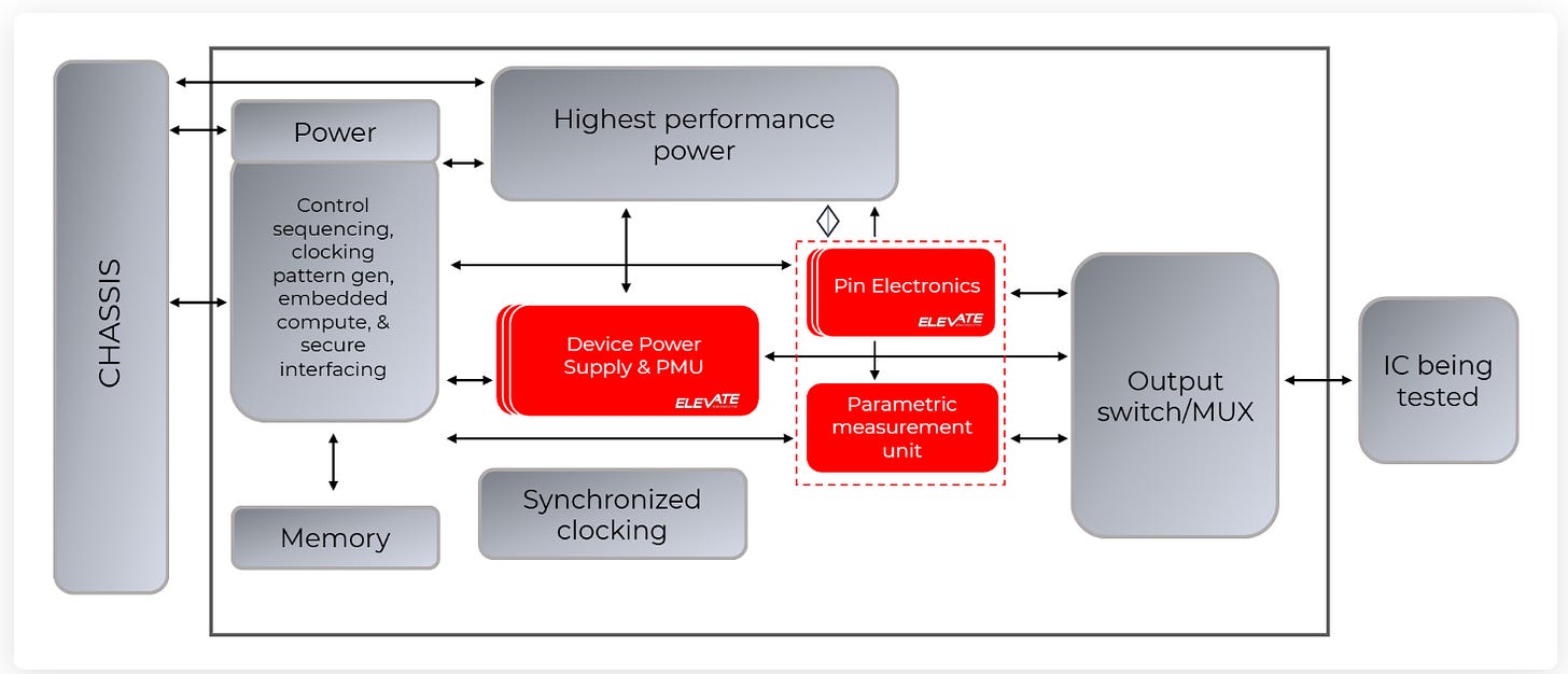
Critical IC building blocks include:
關鍵的 IC 建構模組包括:
Pin Electronics針腳電子元件
PMUsPMU
DPS
DACsDAC
ADCsADC
switching ICs切換式 IC
timing ICs時序 IC
high-voltage interfaces高壓介面
analog front ends類比前端
This creates a second-order AI opportunity.
這創造了第二波的 AI 商機。
AI drives more sophisticated semiconductor test.
AI 推動更精密的半導體測試。
More sophisticated semiconductor test drives higher-performance ATE.
更精密的半導體測試驅動更高性能的 ATE。
Higher-performance ATE requires more capable analog and mixed-signal ICs.
更高效能的自動測試設備(ATE)需要更強大的類比與混合訊號 IC。
That means the demand chain looks something like this:
這意味著需求鏈大致如下:
AI Compute GrowthAI 運算成長
→ Higher Device Complexity
→ 裝置複雜度提升
→ More Test Insertions→ 測試插入點增加
→ Higher ATE Utilization→ 更高的 ATE 利用率
→ More Channels / More Parallelism
→ 更多通道/更高平行度
→ More Semiconductor Content Inside the Tester
→ 測試機內部整合更多半導體內容
ElevATE sits near the end of this chain.
ElevATE 位於此價值鏈的末端附近。
Its core product strategy—higher density, lower power, and greater parallel test capability—is directly aligned with the economics of next-generation ATE.
其核心產品策略——更高密度、更低功耗與更強的平行測試能力,直接契合次世代自動測試設備(ATE)的經濟效益。
Parallelism is particularly important.
平行處理能力尤為重要。
If one tester can test more devices simultaneously, customers can offset part of the rising test burden by lowering cost per device.
若一台測試機可同時測試更多裝置,客戶便能透過降低每顆裝置的測試成本,來抵銷部分日益增加的測試負擔。
This is why channel density is not simply a specification.
這正是通道密度不僅僅是一項規格的原因。
It is an economic variable.
它是一項經濟變數。

Diodes Is Buying Margin Mix, Not Just Revenue
Diodes 收購的是利潤組合,而不僅是營收
The financial details make the strategic logic more obvious.
財務細節讓其戰略邏輯更加清晰。
Diodes previously indicated that ElevATE could contribute approximately US$50 million in revenue during the first 12 months after closing.
Diodes 先前表示,ElevATE 在交易完成後的首 12 個月內可貢獻約 5,000 萬美元的營收。
The company also expects ElevATE to grow at a revenue CAGR above 20% over the following four years.
該公司亦預期 ElevATE 在隨後四年內的營收年複合成長率(CAGR)將超過 20%。
More importantly, ElevATE’s gross margin profile is expected to be materially above Diodes’ corporate average.
更重要的是,ElevATE 的毛利率預估將顯著高於 Diodes 的公司平均值。
That tells us what Diodes is really buying.
這說明了 Diodes 真正收購的是什麼。
It is not primarily buying scale.
這主要不是為了擴大規模。
It is buying:該公司正在收購:
higher-margin analog exposure,
更高利潤的類比產品佈局,
more specialized application-specific products,
更專業的特定應用產品,
stronger design-in economics,
更強勁的設計導入經濟效益,
and a pathway into semiconductor test infrastructure.
以及邁向半導體測試基礎設施的路徑。
This is a portfolio-mix transaction.
這是一項產品組合混合的交易。
Diodes has historically had broad exposure across discrete, analog, logic, and power products.
Diodes 歷來在離散元件、類比、邏輯及電源產品領域擁有廣泛的佈局。
ElevATE gives it a foothold in a narrower but more technically demanding segment.
ElevATE 讓其得以切入一個更狹窄但技術要求更高的細分市場。
That is strategically attractive because specialized ATE ICs typically have:
此舉具戰略吸引力,因為專用的自動測試設備(ATE)IC 通常具備以下特點:
long qualification cycles,
漫長的認證週期,
sticky design wins,高黏著度的設計導入,
demanding performance specifications,
嚴苛的性能規格,
high reliability requirements,
高度的可靠性要求,
and relatively high switching costs.
以及相對較高的轉換成本。
Once designed into a tester architecture, these components may remain in production for years.
一旦這些元件被設計進測試機架構中,可能會持續量產多年。
This creates a better business profile than many lower-differentiation analog categories.
這使其業務概況優於許多差異化程度較低的類比產品類別。
ATE Is Already Showing AI-Driven Operating Leverage
ATE 已展現 AI 驅動的營運槓桿效應
The broader ATE market is already confirming the thesis.
更廣泛的自動測試設備(ATE)市場已證實此論點。
Advantest has benefited from rising AI compute and memory test demand.
愛德萬測試(Advantest)已受惠於人工智慧運算與記憶體測試需求的增长。
Teradyne has seen strong growth in semiconductor test, with AI compute and memory acting as major drivers.
泰瑞達(Teradyne)在半導體測試領域見證強勁成長,其中人工智慧運算與記憶體為主要驅動因素。
HBM is especially important.
高頻寬記憶體(HBM)尤為重要。

HBM requires more intensive memory testing than commodity DRAM because:
HBM 需要比標準 DRAM 更密集的記憶體測試,原因如下:
stack-level yield matters,
堆疊層級的良率至關重要,
pre-bond screening matters,
鍵合前的篩選至關重要,
thermal behavior matters,
熱行為至關重要,
interfaces are more complex,
介面更加複雜,
and the final package carries much more value.
且最終封裝承載的價值大幅提升。
This is why memory test revenue has become more strategically important in the current AI cycle.
這正是記憶體測試營收在當前 AI 週期中變得更具戰略重要性的原因。
The first major AI hardware bottlenecks were:
首批主要的 AI 硬體瓶頸包括:
GPU → HBM → CoWoS
The next bottlenecks are increasingly spreading into:
接下來的瓶頸正日益擴散至:
ATE → Probe Card → Probe Interface → Test Socket → Handler → Burn-In → SLT → Thermal Control → Optical Test
ATE → 探針卡 → 探針介面 → 測試插座 → 處理機 → 老化測試 → 系統級測試(SLT)→ 熱控制 → 光學測試
This is the next layer of the AI infrastructure stack.
這是 AI 基礎設施堆疊的下一個層級。
It is smaller than GPUs.
其規模小於 GPU。
But its growth rate and strategic importance are increasing.
但其成長率與戰略重要性正持續提升。

The Next Shift: From Standalone Test to Integrated Test
下一波變革:從獨立測試邁向整合測試
There is another structural change that matters.
還有另一項重要的結構性變革。
Test is becoming less fragmented.
測試正變得較不零散。
Historically, wafer test, package test, system-level test, and reliability screening could be treated as separate manufacturing steps.
過去,晶圓測試、封裝測試、系統層級測試與可靠性篩選可被視為獨立的製造步驟。
Advanced packaging makes this separation less practical.
先進封裝技術使這種分離做法變得更不切實際。
A chiplet-based architecture requires continuous quality tracking from wafer to system.
基於小晶片(chiplet)的架構需要從晶圓到系統進行持續的品質追蹤。
That creates a more integrated test model:
這催生了更整合的測試模式:
Wafer Test晶圓測試
→ Die-Level Characterization
→ 晶粒級特性分析
→ Pre-Bond Screening→ 接合前篩選
→ Assembly Test→ 組裝測試
→ Package Test→ 封裝測試
→ System-Level Test→ 系統層級測試
→ Reliability Feedback→ 可靠性回饋
The important word is not “test.”
關鍵詞並非「測試」。
It isfeedback.而是回饋。
The future value of test equipment will increasingly come from data.
測試設備的未來價值將日益來自數據。
A tester can generate information that feeds back into:
測試機可產生資訊,回饋至:
wafer process control,晶圓製程控制,
bonding optimization,接合優化,
warpage management,翹曲管理,
thermal process tuning,熱製程調校,
assembly yield improvement,
組裝良率提升,
package reliability,封裝可靠度,
and failure analysis.與故障分析。
This turns test infrastructure into a manufacturing-data layer.
這將測試基礎設施轉變為製造數據層。
That is strategically important because modern AI packages are too complex to optimize purely through end-of-line inspection.
這一點具有戰略重要性,因為現代的 AI 封裝過於複雜,無法僅透過產線末端檢測來進行最佳化。
Manufacturers need closed-loop feedback.
製造商需要閉迴路回饋機制。
The tester becomes part of that loop.
測試機成為該迴路的一部分。
Test Data Could Become a New Competitive Layer
測試數據可能成為新的競爭層面
This trend is still early.
此趨勢仍處於早期階段。
But it could become one of the more important changes in semiconductor manufacturing.
但這可能成為半導體製造中更重要的變革之一。
The more test insertions a package has, the more test data is generated.
封裝中的測試插入次數越多,產生的測試數據就越多。
That data can be used for:
這些數據可用於:
adaptive test,自適應測試,
failure prediction,故障預測,
anomaly detection,異常偵測,
bin optimization,分級優化,
yield correlation,良率關聯性,
root-cause analysis,根本原因分析,
and predictive maintenance.
以及預測性維護。
AI may eventually optimize AI-chip test.
AI 最終可能會優化 AI 晶片的測試。
That sounds circular, but it is economically logical.
這聽起來像是循環論證,但在經濟上卻是合乎邏輯的。
The industry is already collecting enormous volumes of manufacturing data.
業界已蒐集龐大的製造數據。
Advanced packaging makes that data even more valuable because failures can emerge from interactions between multiple components.
先進封裝讓這些數據更具價值,因為故障可能源自多個元件之間的相互作用。
The companies that can correlate wafer-level, package-level, and system-level test data may gain an advantage in yield learning.
能夠關聯晶圓級、封裝級與系統級測試資料的公司,可能在良率學習上取得優勢。
This is one reason integrated test platforms could become more strategically important over time.
這是整合測試平台隨時間推移可能變得更具戰略重要性的原因之一。
The Bigger Message From the Diodes–ElevATE Deal
Diodes 收購 ElevATE 所傳達的更大訊息
Diodes’ US$250 million acquisition of ElevATE is not a transformative M&A deal for the semiconductor industry.
Diodes 以 2.5 億美元收購 ElevATE,對半導體產業而言並非一項具轉型意義的併購交易。
But it is an informative one.
但這是一項具啟發性的交易。
It shows capital moving toward a less visible part of the AI supply chain.
這顯示資金正流向人工智慧供應鏈中較不易被察覺的環節。
The old semiconductor investment equation was:
過去半導體投資的方程式是:
More process complexity → more wafer-fab equipment.
製程複雜度提升 → 晶圓廠設備需求增加。
The AI-era equation is increasingly:
AI 時代的方程式正日益演變為:
More system complexity → more test infrastructure.
系統複雜度提升 → 測試基礎設施需求增加。
That distinction matters because the bottleneck is moving.
此區別至關重要,因為瓶頸正在轉移。
As AI chips become larger, hotter, more heterogeneous, and more expensive, manufacturing success is no longer determined only by whether the wafer can be fabricated.
隨著 AI 晶片變得更大、更熱、更具異質性且成本更高,製造成功與否不再僅取決於晶圓能否被製造出來。
It is determined by whether the entire system can be assembled with acceptable yield.
而是取決於整個系統能否以可接受的良率完成組裝。
Test is central to that equation.
測試是此方程式的核心。
And because the value of the final package is rising so quickly, the industry can economically justify spending more to protect that value.
由於最終封裝的價值迅速攀升,產業在經濟上更有理由投入更多資源以保護該價值。
SemiVision ViewSemiVision 視角
The AI test cycle is still underappreciated.
AI 測試週期仍未獲得足夠重視。
Most AI semiconductor analysis remains concentrated around leading-edge wafer starts, HBM bit growth, CoWoS capacity, and accelerator shipments.
大多數 AI 半導體分析仍集中於先進製程晶圓投產量、HBM 位元成長、CoWoS 產能以及加速器出貨量。
Those are still the largest value pools.
這些仍是最大的價值池。
But they are no longer the only ones that matter.
但它們已不再是唯一重要的領域。
We expect test intensity to increase structurally across AI semiconductor architectures.
我們預期,在 AI 半導體架構中,測試強度將出現結構性提升。
This should benefit not only major ATE companies, but also suppliers across:
這不僅將使主要的 ATE 公司受益,也將惠及以下領域的供應商:
ATE analog and mixed-signal ICs,
ATE 類比與混合訊號 IC,
probe cards,探針卡,
test interfaces,測試介面,
sockets,插座、
handlers,處理機、
burn-in systems,老化測試系統、
thermal management,熱管理,
system-level test,系統級測試,
and eventually optical test.
並最終發展至光學測試。
The key question is no longer whether AI increases semiconductor test demand.
關鍵問題已不再是人工智慧是否會增加半導體測試需求。
It does.確實如此。
The more important question is:
更關鍵的問題是:
How quickly does test content grow relative to compute content?
測試內容的成長速度相對於運算內容有多快?
That is the metric investors should watch
這才是投資者應密切關注的指標。
Thanks for reading SEMIVISION @_@! This post is public so feel free to share it.
感謝閱讀 SEMIVISION @_@!本文為公開文章,歡迎自由分享。
As a final note, I attended the CPO Advanced Packaging and Test Forum hosted by ITRI in July. One of the presentations that stood out was from Clark at MJC, who shared a particularly insightful slide on SW Test.
最後補充一點,我於七月參加了由工研院主辦的 CPO 先進封裝與測試論壇。其中令人印象深刻的演講之一,來自 MJC 的 Clark,他分享了一張關於 SW Test 極具洞察力的投影片。

The key message was simple but important: as semiconductor technology scales toward 67 GHz probing, sub-10-second silicon photonics throughput, and increasingly complex CPO architectures, testing can no longer be optimized in isolation.
關鍵訊息簡單卻至關重要:隨著半導體技術邁向 67 GHz 探測、次 10 秒矽光子吞吐量,以及日益複雜的共封裝光學(CPO)架構,測試已無法再孤立地進行優化。
Success increasingly depends on the entire ecosystem working together:
成功日益取決於整個生態系統的協同運作:
Prober + Probe Card + ATE + Optical Alignment + Software
探針台 + 探針卡 + ATE + 光學對準 + 軟體
This is exactly where the test industry is heading. The bottleneck is no longer a single piece of equipment or a single test specification. It is the integration and co-optimization of the entire test environment.
這正是測試產業的發展方向。瓶頸已不再單一設備或單一測試規格,而是整體測試環境的整合與共同優化。
For CPO, chiplets, HBM, and other heterogeneous architectures, the speed of technological scaling will increasingly depend on the density of collaboration across the test ecosystem.
針對 CPO、Chiplet、HBM 及其他異質架構,技術擴展的速度將愈發取決於測試生態系統中協作的密度。
A very good slide—and, in my view, a very accurate description of where semiconductor test is going.
這是一張非常出色的投影片,而且在我看來,它準確地描述了半導體測試的發展方向。


Share分享
Previous上一頁