Hot Chips 2026: The Memory Wall Is Making Hybrid Bonding a Necessity
Hot Chips 2026: The Memory Wall Is Making Hybrid Bonding a Necessity
- Source: SemiVision
- Author: SEMIVISION
- Published: 2026-08-27T10:09:39+08:00
- URL: https://tspasemiconductor.substack.com/p/hot-chips-2026-the-memory-wall-is
中文翻譯與英文原文(雙語)
(2) Hot Chips 2026:記憶體牆正使混合鍵結成為必要技術 --- (2) Hot Chips 2026: The Memory Wall Is Making Hybrid Bonding a Necessity


Hot Chips 2026: The Memory Wall Is Making Hybrid Bonding a Necessity
Hot Chips 2026:記憶體牆正使混合鍵合成為必要技術
Original Article By SemiVision Research [Reading time: 11 mins]
原文作者:SemiVision Research [閱讀時間:11 分鐘]

Aug 27, 2026
∙ Paid∙ 付費
Share分享
Hot Chips 2026: The Memory Wall Is Making Hybrid Bonding a Necessity
Hot Chips 2026:記憶體牆使混合鍵合成為必要技術

If there is one semiconductor trend worth taking away from Hot Chips 2026, it may not be a new GPU or accelerator.
若說 2026 年 Hot Chips 大會最值得關注的半導體趨勢,那可能並非全新的 GPU 或加速器。
It is the growing realization that the next phase of AI performance will increasingly be determined by memory, interconnects, and packaging—not transistor scaling alone.
而是業界日益體認到,下一階段的 AI 效能將愈來愈取決於記憶體、互連技術與封裝,而非僅靠電晶體微縮。

This shift was visible throughout this year’s Hot Chips agenda. Micron discussed Evolving Memory Architectures for AI. Samsung focused on the evolution of the HBM base die. SK hynix presented its roadmap for advanced HBM packaging.
這一轉變在今年的 Hot Chips 議程中清晰可見:美光(Micron)探討了面向 AI 的演進式記憶體架構;三星(Samsung)聚焦於 HBM 基底晶片的演進;SK 海力士(SK hynix)則提出了其先進 HBM 封裝的路線圖。
Put together, the message was surprisingly consistent:
綜合來看,這些訊息呈現出驚人的一致性:
AI’s next bottleneck is moving from compute to data movement.
AI 的下一個瓶頸正從運算能力轉向資料傳輸。
The industry has become very good at adding FLOPS. The harder problem is feeding those compute engines with enough data, at sufficiently low latency and power.
業界已非常擅長增加 FLOPS,但更艱鉅的挑戰在於如何以足夠低的延遲與功耗,為這些運算引擎提供充足的資料。
That is exactly why hybrid bonding is moving toward the center of the AI semiconductor roadmap.
這正是混合鍵合(hybrid bonding)技術逐漸成為 AI 半導體發展路線圖核心的原因。

Final day of@hotchipsorg2026 underway! Today’s sessions include FPGA, memory, networking and interconnect, and AI processors/accelerators. Virtual registration still available athotchips.org/registration/
@hotchipsorg 2026 最後一天正式展開!今日的議程涵蓋 FPGA、記憶體、網路與互連技術,以及 AI 處理器/加速器。虛擬報名仍開放中,請至 hotchips.org/registration/

12:10 AM · Aug 26, 2026·1430 Views
上午 12:10 · 2026 年 8 月 26 日 · 1430 次瀏覽
1 Reply·22 Likes1 則回覆 · 22 個讚
The Memory Wall Is Getting Worse, Not Better
記憶體牆問題正日益惡化,而非改善
One of the most important messages from Hot Chips came from Micron.
Hot Chips 會議中最重要的訊息之一來自 Micron。
AI accelerator compute capability has been increasing at roughly 3× every two years, while HBM bandwidth has historically improved at less than 2× over a comparable period.
AI 加速器的運算能力大約每兩年提升 3 倍,而 HBM 頻寬在可比期間的歷史增幅則不到 2 倍。
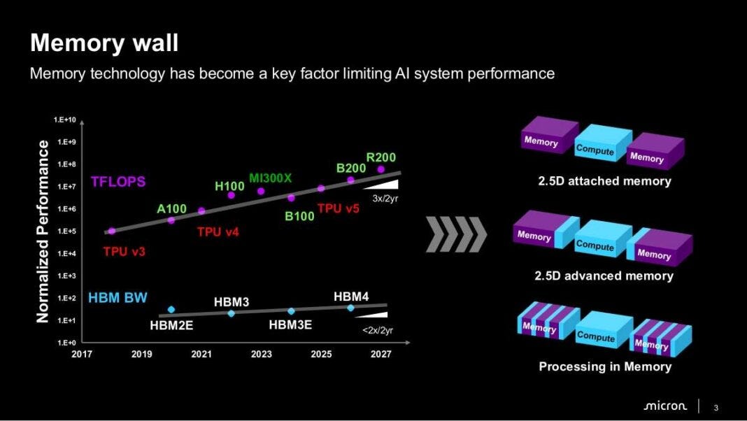
That gap matters.此差距至關重要。
Below we will share:以下我們將分享:
The Hot Chips Surprise: Hybrid Bonding May Arrive Later Than Expected
Hot Chips 的意外發現:混合鍵合技術的到來時間可能晚於預期
W2W or D2W? The Real Battle Is Yield
W2W 還是 D2W?真正的戰場在於良率
HBM’s Real Future Is Not Just Hybrid Bonding. It Is 3D.
HBM 的真正未來不僅是混合鍵合,更是 3D 技術。
The Hardest Problem May Eventually Be Heat
最艱鉅的挑戰最終可能來自散熱問題。
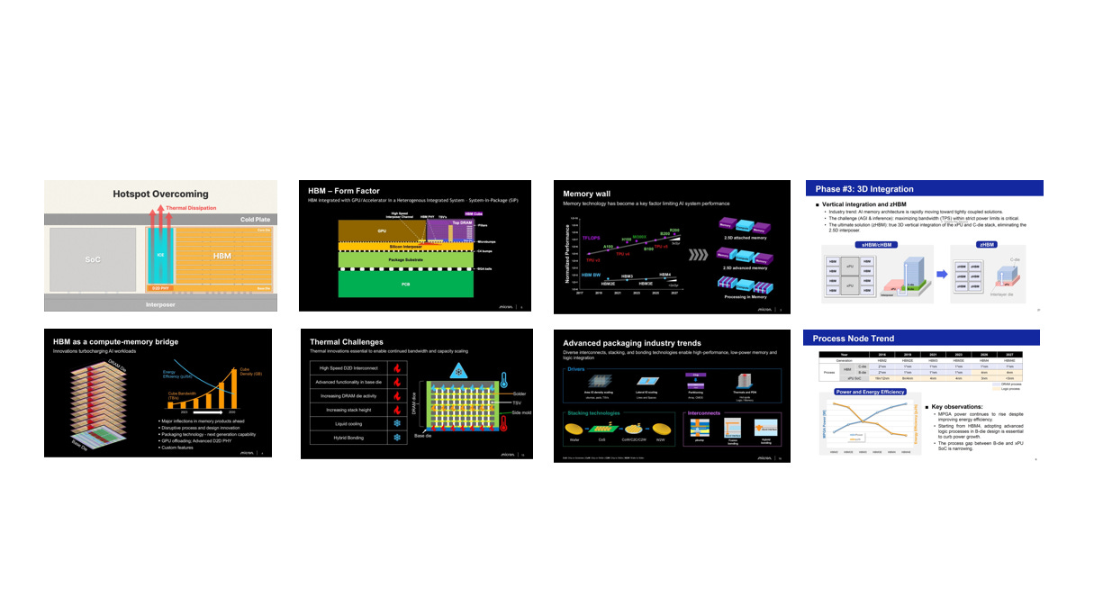

7月2日7 月 2 日

2月5日2 月 5 日
A GPU can contain more tensor cores, larger matrix engines, and higher theoretical throughput. But if memory cannot supply data quickly enough, those compute units spend more time waiting.
GPU 可以容納更多的張量核心、更大的矩陣引擎,以及更高的理論吞吐量。但如果記憶體無法足夠快速地提供資料,這些運算單元就會花費更多時間等待。
In other words, the famous memory wall has not disappeared.
換言之,著名的記憶體牆並未消失。
It may actually be getting worse.
情況甚至可能更加惡化。
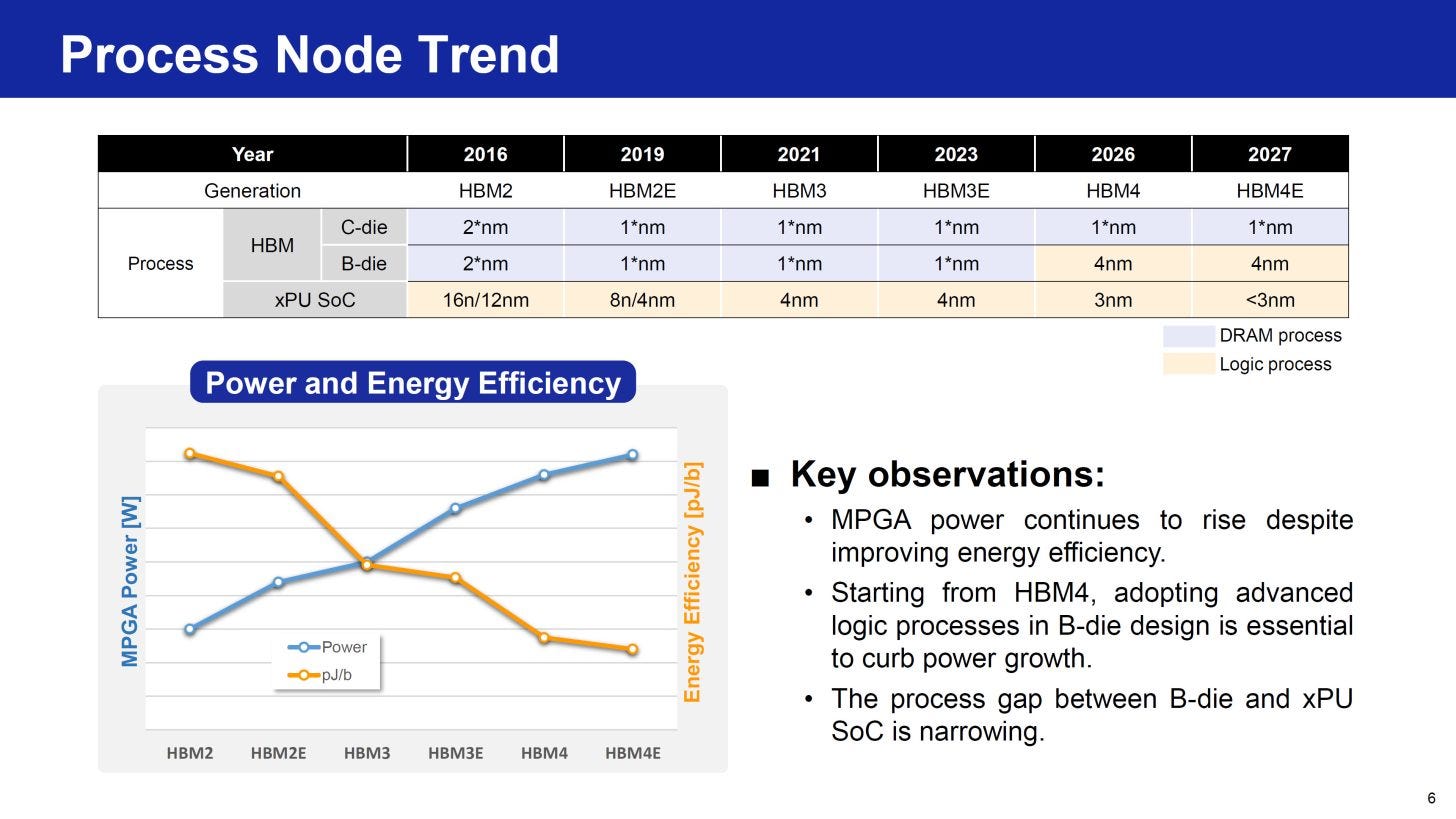
HBM4 is an important step forward. The interface expands from 1,024 I/Os in previous HBM generations to 2,048 I/Os, substantially increasing bandwidth.
HBM4 是邁向未來的重要一步。其介面從先前 HBM 世代的 1,024 個 I/O 擴增至 2,048 個 I/O,大幅提升頻寬。
Micron has already demonstrated HBM4 bandwidth above 2.8 TB/s per stack.
Micron 已成功展示每堆疊 HBM4 頻寬超過 2.8 TB/s。
But even that does not entirely keep pace with the rate at which AI compute performance is scaling.
但即便如此,仍無法完全跟上 AI 運算效能的擴展速度。
This is why the industry is increasingly looking beyond conventional memory scaling.
這正是產業界日益轉向超越傳統記憶體擴展方案的原因。
More I/O is required.需要更多的 I/O。
Shorter interconnects are required.
需要更短的互連。
Lower power per bit is required.
需要降低每位元的功耗。
And eventually, memory may need to move physically closer to the compute die.
最終,記憶體可能需要物理上更靠近運算晶片。
Hybrid bonding addresses all four.
混合鍵合技術可同時解決這四項挑戰。
From 100 µm to 20 µm—and Eventually Toward 2 µm
從 100 µm 到 20 µm,並最終邁向 2 µm
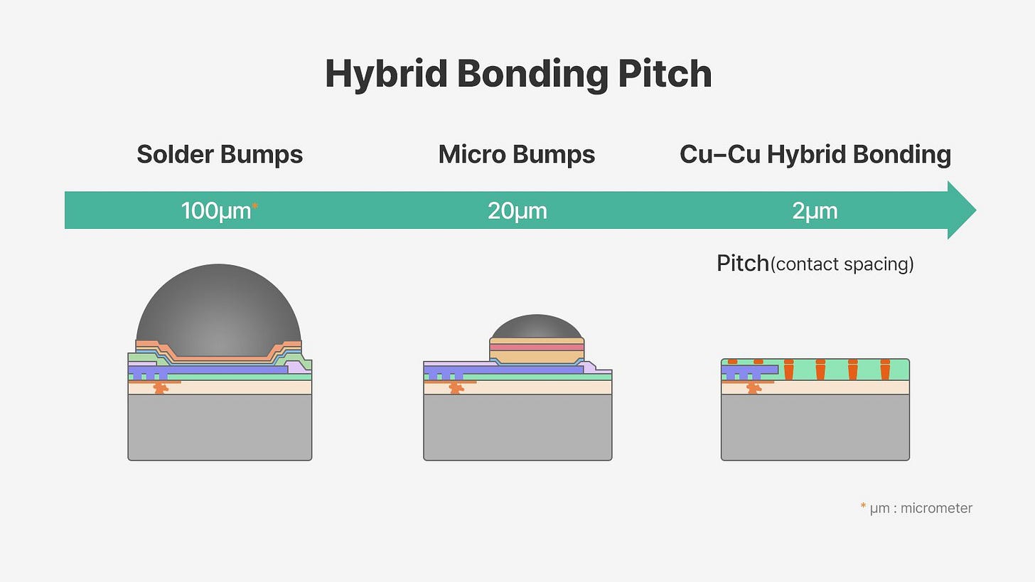
The easiest way to understand hybrid bonding is to look atinterconnect pitch.
理解混合鍵合最簡單的方式是觀察互連間距。
Traditional solder bumps operate at roughly the hundred-micron scale.
傳統焊錫凸塊的運作尺度約為百微米等級。
Advanced micro-bumps have pushed interconnect pitch into the tens-of-microns range.
先進微凸塊已將互連間距推進至數十微米範圍。
Cu-Cu hybrid bonding can go much further, potentially into single-digit microns and, at the leading edge, toward2 µm and below.
銅 - 銅混合鍵合可進一步大幅縮小間距,潛在可達個位數微米,而在最先進製程中更朝向 2 µm 及以下發展。
This is much more significant than simply “making bumps smaller.”
這遠比單純「縮小凸塊」更為重要。
As pitch shrinks, the number of electrical connections that can be placed within a given area increases dramatically.
隨著間距縮小,單位面積內可容納的電氣連接數量大幅增加。
At the same time, hybrid bonding eliminates much of the solder structure and gap associated with conventional micro-bump connections.
同時,混合鍵合技術消除了傳統微凸塊連接所伴隨的大部分銲料結構與間隙。
The distance between two dies becomes significantly smaller.
兩顆晶粒之間的距離顯著縮短。
That changes the nature of semiconductor packaging.
這改變了半導體封裝的本質。
Instead of merely connecting two chips, advanced packaging begins to make two separate pieces of silicon behave increasingly like one integrated device.
先進封裝不僅僅是連接兩顆晶片,更讓兩塊獨立的矽晶圓表現得愈發像單一整合裝置。
However, one distinction is essential.
然而,有一項區別至關重要。

Technology capability is not the same as mass-production capability.
技術能力不等於量產能力。
Although 2 µm and even sub-micron hybrid-bonding pitches have been demonstrated in advanced R&D environments, that does not mean mass-produced HBM is already using 2 µm interconnects.
儘管在先進研發環境中已展示出 2 µm 甚至次微米級的混合鍵合間距,但這並不表示量產的 HBM 已經採用 2 µm 的互連技術。
According to SK hynix’s Hot Chips discussion, current MR-MUF HBM structures remain around the tens-of-microns range. Hybrid bonding becomes particularly attractive as future HBM moves toward 20-high stacks and tighter vertical interconnect geometries.
根據 SK hynix 在 Hot Chips 的討論,目前的 MR-MUF HBM 結構仍維持在數十微米的範圍。隨著未來 HBM 朝向 20 層堆疊及更緊密的垂直互連幾何結構發展,混合鍵結(Hybrid Bonding)技術將變得極具吸引力。
So the technical frontier has already moved far ahead.
因此,技術前沿已經大幅領先。
The manufacturing frontier still has to catch up.
製造前沿仍須迎頭趕上。
And the difference between the two comes down to three things:
而兩者之間的差異可歸結為三項因素:
yield, throughput, and cost.
良率、產能與成本。
The Hot Chips Surprise: Hybrid Bonding May Arrive Later Than Expected
Hot Chips 驚喜:混合鍵合技術的到來可能比預期更晚
For the past two years, there has been growing market speculation that hybrid bonding could quickly become necessary for HBM4 or HBM4E.
過去兩年,市場日益猜測混合鍵合(hybrid bonding)可能會迅速成為 HBM4 或 HBM4E 的必要技術。
Hot Chips 2026 offered a more cautious picture.
Hot Chips 2026 呈現了更為謹慎的展望。
One of the fundamental constraints facing HBM is package height.
HBM 面臨的基本限制之一是封裝高度。
The overall HBM stack must remain within a strict vertical envelope. As DRAM stacks increase from 12-high toward 16-high, 20-high and potentially beyond, each individual die must become thinner.
整體 HBM 堆疊必須保持在嚴格的垂直範圍內。隨著 DRAM 堆疊從 12 層增加至 16 層、20 層甚至更高,每個單獨的晶粒都必須变得更薄。
For 16-high HBM4, DRAM dies are already being pushed toward extremely thin dimensions.
對於 16 層的 HBM4,DRAM 晶粒已經被推向極薄的尺寸。

Hybrid bonding is attractive because eliminating conventional micro-bumps can reduce the vertical spacing between dies.
混合鍵合之所以具吸引力,是因為消除傳統微凸塊可減少晶粒間的垂直間距。
In theory, this makes it an excellent technology for very high HBM stacks.
理論上,這使其成為超高堆疊 HBM 的絕佳技術。
But an important change has given conventional HBM packaging additional room to evolve: the package-height specification has been relaxed.
但一項重要變革為傳統 HBM 封裝提供了更多演進空間:封裝高度規範已放寬。
This allows existing technologies such as SK hynix’sMR-MUFprocess to remain competitive longer than many expected.
這使得現有技術(例如 SK hynix 的 MR-MUF 製程)能夠比許多預期更長時間保持競爭力。
The implication from Hot Chips was therefore notable:
因此,Hot Chips 會議所傳達的意涵尤為顯著:
HBM4E may not require hybrid bonding after all.
HBM4E 可能終究無需混合鍵合技術。
Instead, the more meaningful transition could occur aroundHBM5 and 20-high HBM.
相反,更具意義的轉變可能發生在 HBM5 與 20 層堆疊的 HBM 階段。
That may sound bearish for hybrid bonding.
這聽起來似乎對混合鍵結(hybrid bonding)技術不利。
It is actually the opposite.
但事實恰恰相反。
The Hot Chips presentations suggested that hybrid bonding is becoming increasingly inevitable—but perhaps not immediately.
Hot Chips 研討會中的演講指出,混合鍵結正變得日益不可避免——儘管未必會立即實現。
That distinction matters for investors and equipment suppliers.
此區別對投資者和設備供應商至關重要。
The technology’s strategic importance is rising faster than its near-term production adoption.
該技術的戰略重要性提升速度,快於其短期內的生產採用速度。

2025年7月13日2025 年 7 月 13 日
W2W or D2W? The Real Battle Is Yield
W2W 還是 D2W?真正的戰場在於良率
There are two major approaches to hybrid bonding:
混合鍵合主要有兩種方法:
Wafer-to-Wafer, or W2W, andDie-to-Wafer, or D2W.
晶圓對晶圓(Wafer-to-Wafer,簡稱 W2W)與晶粒對晶圓(Die-to-Wafer,簡稱 D2W)。
W2W offers an obvious manufacturing advantage: throughput.
W2W 提供了一項顯著的製造優勢:產出量。

Two wafers can undergo CMP, cleaning, surface activation, precision alignment and bonding before being processed together.
兩片晶圓可先共同進行 CMP、清洗、表面活化、精密對準與接合,之後再一併進行後續製程。
Thousands of dies can effectively be bonded in a single wafer-level operation.
數千顆晶粒可在單一晶圓級製程中有效接合。
For applications where both wafers have similar die sizes and mature yields, this approach can be extremely efficient.
對於兩片晶圓具有相似晶粒尺寸且良率成熟的應用,此方法極為高效。
CMOS image sensors are one of the best examples.
CMOS 影像感測器便是最佳範例之一。
But W2W has a fundamental weakness.
然而,晶圓對晶圓(W2W)技術存在一項根本性弱點。
If one wafer contains a bad die, that die may be permanently bonded to a good die on the other wafer.
若其中一片晶圓包含不良晶粒,該不良晶粒可能會永久鍵結至另一片晶圓上的良好晶粒。
For low-cost devices, that may be acceptable.
對於低成本裝置而言,這或許是可以接受的。
For expensive AI processors and advanced memory, it becomes much more painful.
對於昂貴的 AI 處理器與先進記憶體而言,這種情況將變得更加嚴峻。
This is whyDie-to-Wafer bonding becomes strategically important.
這就是晶粒對晶圓(Die-to-Wafer, D2W)鍵合技術變得具有戰略重要性的原因。
With D2W, manufacturers can test dies first, identify Known Good Dies, and then selectively place only qualified dies onto the target wafer.
透過 D2W 技術,製造商可以先對晶粒進行測試,識別出已知良好晶粒(Known Good Dies),然後僅將符合資格的晶粒選擇性地置放於目標晶圓上。
The economics are particularly attractive when each individual chip is expensive.
當每顆個別晶片成本高昂時,此技術的經濟效益尤為顯著。

That makes D2W highly relevant to:
這使得晶粒對晶圓(D2W)技術與以下領域高度相關:
HBM
advanced logic先進邏輯
chiplets小晶片
heterogeneous integration
異質整合
3D logic stacking3D 邏輯堆疊
The trade-off is manufacturing complexity.
其代價是製造複雜度。
Individual dies must be handled, positioned and aligned at extremely high speed and accuracy.
必須以極高的速度和精度來處理、定位並對齊個別晶粒。
As bonding pitch moves into the few-micron range, even tiny placement errors become unacceptable.
隨著接合間距縮小至數微米範圍,即使是微小的對位誤差也變得無法接受。
Therefore, the real hybrid-bonding equipment battle will not simply be about who has the best alignment specification.
因此,真正的混合鍵合設備競爭將不僅僅取決於誰擁有最佳的對準規格。
It will be about who can simultaneously deliver:
關鍵在於誰能同時實現:
alignment accuracy + particle control + die handling + throughput + yield.
對準精度+微粒控制+晶粒處理+產出量+良率。
A machine with spectacular laboratory precision but insufficient production throughput will not win.
一台在實驗室中展現卓越精度但生產產出量不足的設備,終將無法勝出。
Nor will a high-throughput machine that destroys yield.
也不會採用會破壞良率的高產能機台。
The winner will be the company that finds the manufacturing sweet spot.
勝出者將是找到製造甜蜜點的公司。

HBM’s Real Future Is Not Just Hybrid Bonding. It Is 3D.
HBM 的真正未來不僅僅是混合鍵合,而是 3D 技術。
Another important development at Hot Chips came from Samsung.
Hot Chips 會議上的另一項重要進展來自三星。
The HBM base die is beginning to change.
HBM 基底晶圓正開始發生變化。
Traditionally, the base die mainly serves as an interface layer between stacked DRAM and the accelerator.
傳統上,基底晶粒主要作為堆疊 DRAM 與加速器之間的介面層。
But HBM4 is already pushing the base die toward more advanced logic processes.
但 HBM4 已推動基底晶粒朝向更先進的邏輯製程發展。
Once that happens, an obvious question emerges:
一旦這種情況發生,一個顯而易見的問題便隨之浮現:
Why should the HBM base die remain relatively passive?
為何 HBM 基底晶粒應保持相對被動?
If it is already fabricated using advanced logic technology, more intelligence can potentially move into it.
若其已採用先進邏輯製程製造,則可將更多智慧功能整合其中。
Memory controllers can move closer to DRAM.
記憶體控制器可更靠近 DRAM。
Data-processing functions can move closer to memory.
資料處理功能可更靠近記憶體。
Some compute functions may eventually move into the memory subsystem itself.
部分運算功能最終可能會移至記憶體子系統內部。
This is the beginning of custom HBM.
這是客製化 HBM 的開端。
And Samsung’s longer-term vision goes even further.
而三星的長期願景更為遠大。
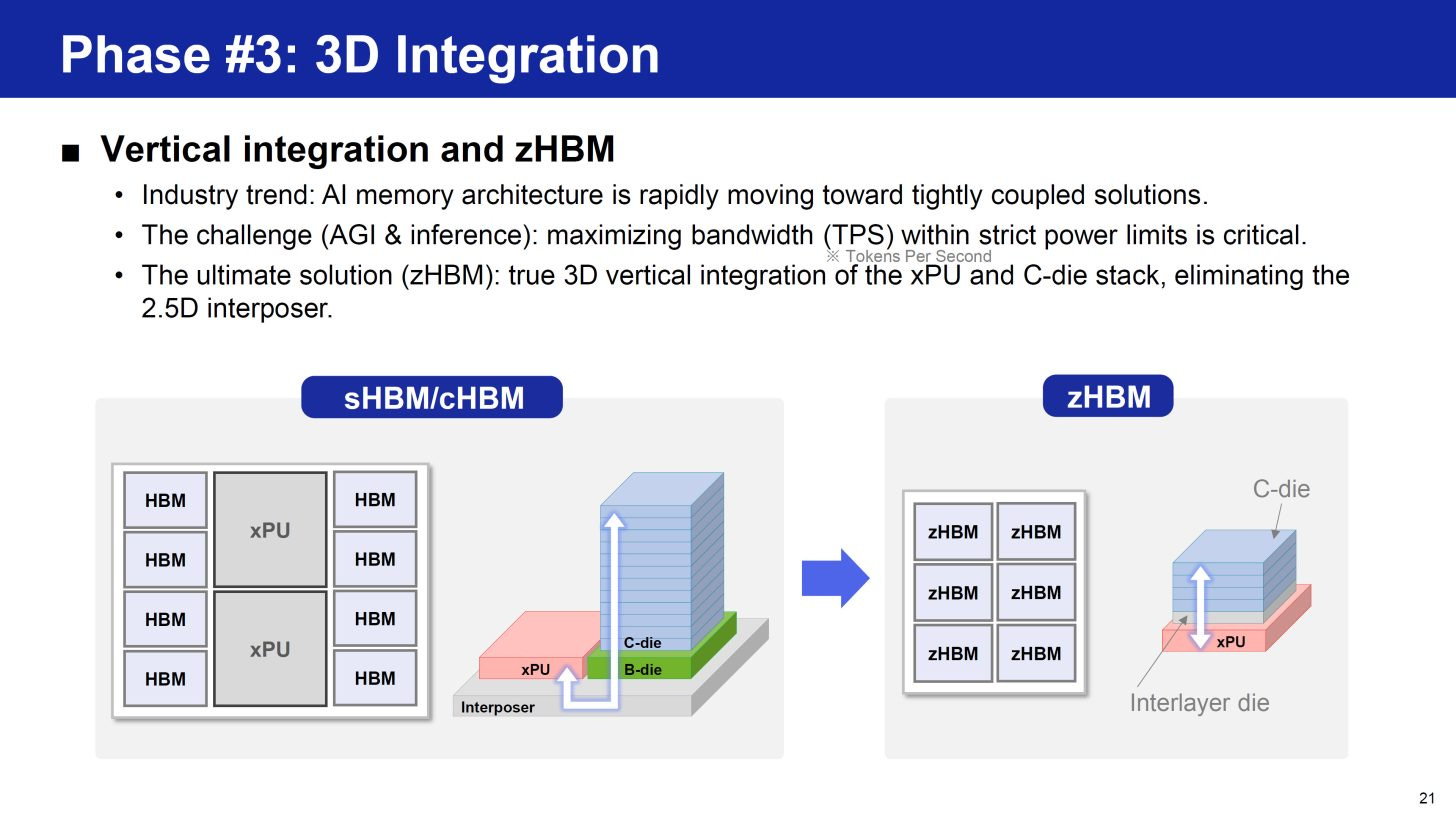
Its recently disclosed zHBM concept explores vertically stacking memory directly above an AI accelerator.
其近期揭露的 zHBM 概念,探索將記憶體直接垂直堆疊於 AI 加速器之上。
Today’s HBM is predominantly a 2.5D architecture:
現今的 HBM 主要採用 2.5D 架構:
GPU | HBM | HBM | HBM
All of these sit side by side on an interposer or advanced redistribution platform.
所有這些元件並排置於中介層或先進重佈層平台上。
The longer-term architecture could look more like:
長期架構可能更類似於:
HBM
HBM
HBM
AI AcceleratorAI 加速器
Memory moves from beside the processor to above it.
記憶體從處理器旁側移至其上方。
That fundamentally changes the role of hybrid bonding.
這從根本上改變了混合鍵合(hybrid bonding)的角色。
It is no longer simply an alternative bumping process.
它已不再僅僅是一種替代性的凸塊製程。
It becomes an enabling technology for3D system architecture.
它成為實現 3D 系統架構的關鍵技術。

8月5日8 月 5 日
The Hardest Problem May Eventually Be Heat
最艱難的挑戰最終可能是散熱問題
As HBM moves toward 16-high and 20-high structures, electrical connectivity is not the only challenge.
隨著 HBM 朝向 16 層與 20 層堆疊結構發展,電氣連接並非唯一的挑戰。
Thermal management may become even more important.
熱管理可能變得更加重要。
The irony of HBM architecture is that some of the hottest circuitry is located near the bottom of the stack—particularly around the logic base die and high-speed PHY.
HBM 架構的弔詭之處在於,部分最發熱的電路位於堆疊的底部附近——特別是邏輯基底晶粒與高速實體層(PHY)周圍。
The main heat sink, meanwhile, is located above the package.
與此同時,主要的散熱片則位於封裝上方。
So the thermal path can become:
因此,熱傳導路徑可能成為:
hot logic → many DRAM layers → heat spreader → cooling system
發熱邏輯 → 多層 DRAM → 散熱片 → 冷卻系統
The taller the HBM stack becomes, the more difficult this problem gets.
HBM 堆疊越高,此問題就越發嚴峻。
Hybrid bonding helps because removing micro-bumps and reducing inter-die gaps can improve the thermal path.
混合鍵結有助於改善散熱路徑,因為它能移除微凸塊並縮減晶粒間的間隙。
It can also allow individual DRAM dies to remain thicker while keeping the complete HBM stack within the same height limit.
此技術亦能讓個別 DRAM 晶粒維持較厚,同時使完整的 HBM 堆疊仍符合相同的高度限制。

2025年10月13日2025 年 10 月 13 日
SK hynix has indicated that, in future very-high-stack HBM configurations, hybrid bonding could enable thicker dies and reduce thermal resistance compared with conventional MR-MUF structures.
SK hynix 表示,在未來極高堆疊的 HBM 配置中,混合鍵結(hybrid bonding)技術相比傳統的 MR-MUF 結構,能夠實現更厚的晶粒並降低熱阻。

SK Hynix: With the iHBM solution, the company has taken a structural approach to addressing the heat management issue. Existing HBM products rely on an indirect cooling method that draws heat away through the core die. In contrast, the iHBM solution places ICEs directly in the D2D PHY area where heat concentration is the highest, creating an additional ‘heat dissipation path’. This latest heat management solution helps reduce thermal resistance by 30% and enables chips to operate stably even in high-temperature and high-pressure conditions.
SK Hynix:透過 iHBM 解決方案,該公司採取了結構化方法來解決散熱管理問題。現有的 HBM 產品依賴間接冷卻方式,將熱量從核心晶粒導出。相較之下,iHBM 解決方案將 ICE 直接置於熱集中程度最高的 D2D PHY 區域,從而建立額外的「散熱路徑」。這項最新的散熱管理解決方案有助於降低 30% 的熱阻,使晶片即使在高溫與高壓條件下也能穩定運作。
SK hynix unveils ‘iHBM’ thermal solution to boost AI performance
Samsung is taking another approach.
三星則採取另一種方法。
The company has discussed adding dedicated Heat Path Blocks near HBM PHY hotspots to create more direct paths for heat removal.
該公司已討論在 HBM PHY 熱點附近新增專用的散熱路徑區塊,以建立更直接的散熱路徑。
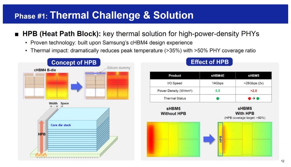
This points to a major architectural transition.
這標誌著一場重大的架構轉型。
In traditional semiconductor development, engineers could design the chip first and solve cooling afterward.
在傳統的半導體開發中,工程師可以先設計晶片,之後再解決散熱問題。
That approach is becoming increasingly difficult for AI.
這種方法對於 AI 來說正變得愈來愈困難。
Future HBM development will need to co-optimize:
未來的 HBM 開發需要進行共同最佳化:
silicon floorplan矽晶圓佈局
PHY placementPHY 配置
base-die architecture基底晶片架構
bonding structure接合結構
package materials封裝材料
thermal interfaces熱介面
liquid cooling液冷散熱
Thermal design is becoming architecture design.
熱設計正逐漸成為架構設計。

Be Careful With the “100×” Hybrid-Bonding Claims
謹慎看待「100 倍」混合鍵合宣稱
Hybrid-bonding presentations often contain impressive figures:
混合鍵結的簡報中常出現令人印象深刻的數據:
15× higher interconnect density.
互連密度提升 15 倍。
11.9× higher speed.速度提升 11.9 倍。
More than 100× improvement in certain performance metrics.
特定效能指標改善超過 100 倍。
Those numbers need context.
這些數字需要背景脈絡來解讀。
Industry material from equipment suppliers such as Besi has shown that hybrid bonding can dramatically increase interconnect density and bandwidth density compared with conventional micro-bump-based chip-to-wafer thermocompression bonding.
來自設備供應商(如 Besi)的產業資料顯示,與傳統的基於微凸塊(micro-bump)之晶片對晶圓(chip-to-wafer)熱壓鍵合相比,混合鍵合(hybrid bonding)能大幅提升互連密度與頻寬密度。
But one number is frequently misunderstood.
但有一個數字經常被誤解。
A claimed 100× improvement does not mean that hybrid bonding improves heat dissipation by 100×.
宣稱的 100 倍改善,並不意味著混合鍵合可將散熱能力提升 100 倍。
The figure refers to a broader Energy Efficient Performance metric.
該數值指的是更廣泛的「能源效率效能」(Energy Efficient Performance)指標。
Thermal improvement is significant, but nowhere near a literal 100-fold gain in heat-dissipation capability.
散熱效能雖有顯著提升,但距離實際的百倍散熱能力仍有很大差距。
This distinction is important because hybrid bonding is becoming one of the most heavily marketed technologies in advanced packaging.
此區別至關重要,因為混合鍵結正成為先進封裝中最受矚目的技術之一。
The trend is real.趨勢確實存在。
The physics are compelling.
物理原理令人信服。
But the metrics still need to be separated from the marketing.
但指標仍需與行銷說辭區分開來。
The Next Equipment Cycle Is Bigger Than the Hybrid Bonder
下一輪設備週期的規模將超越混合鍵合機本身。
From a supply-chain perspective, perhaps the most interesting implication is that the hybrid-bonding opportunity extends far beyond the bonding machine itself.
從供應鏈的角度來看,或許最有趣的影響在於,混合鍵合(hybrid bonding)的商機遠不止於鍵合機本身。
A production hybrid-bonding flow may require:
一個量產級的混合鍵合製程可能需要:
CMP and surface planarization
化學機械拋光(CMP)與表面平坦化
ultra-clean wafer cleaning
超潔淨晶圓清洗
plasma activation電漿活化
particle inspection微粒檢測
precision alignment精密對準
wafer bonding晶圓接合
die-to-wafer bonding晶圓對晶片接合
annealing退火
wafer thinning晶圓減薄
temporary bonding and debonding
臨時接合與解接合
plasma dicing電漿切割
post-bond inspection鍵合後檢測
defect metrology缺陷量測
As pitch moves from tens of microns toward single-digit microns, contamination requirements become dramatically tougher.
隨著間距從數十微米縮減至個位數微米,對污染控制的要求變得極為嚴苛。
At these dimensions, a tiny particle can prevent proper bonding and create a void large enough to kill an interface.
在這些尺寸下,微小的顆粒就可能阻礙正確接合,並產生足以毀壞介面的空洞。
This means advanced packaging is increasingly adopting manufacturing requirements that look more like front-end semiconductor processing.
這意味著先進封裝正日益採用更接近半導體前段製程的製造要求。
The competitive advantage will therefore shift from individual tool specifications toward something much harder to replicate:
因此,競爭優勢將從單一設備規格,轉向更難以複製的領域:
process integration and yield learning.
製程整合與良率學習。
The companies that understand the entire bonding flow—not simply one machine—could capture disproportionate value.
能夠掌握完整接合流程(而不僅是單一設備)的公司,將能獲取不成比例的價值。
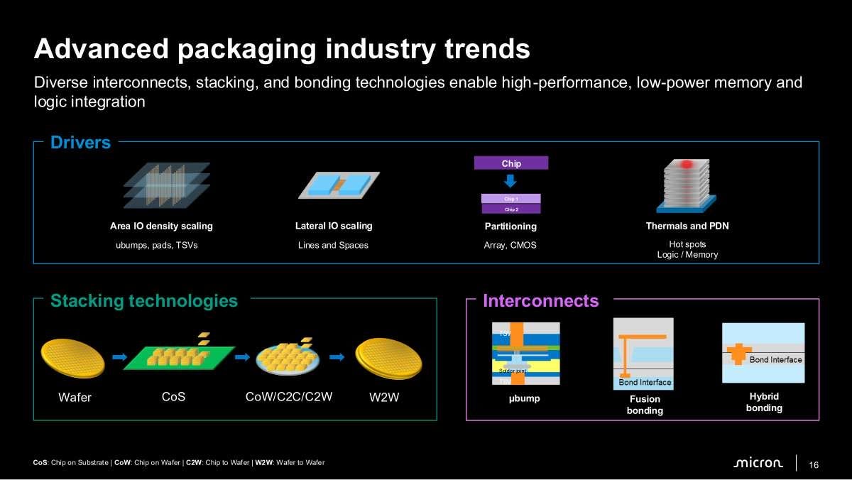
HBM Is Gradually Becoming a System Chip
HBM 正逐漸演變為系統晶片
If we combine the messages from Micron, Samsung and SK hynix at Hot Chips 2026, the direction becomes clear.
若我們將美光、三星與 SK hynix 在 Hot Chips 2026 所傳達的訊息綜合起來,發展方向便清晰可見。
Micron is effectively saying:
美光實質上表示:
The memory wall is getting worse.
記憶體牆問題日益嚴峻。
SK hynix is saying:SK hynix 則表示:
Traditional micro-bump architectures will eventually run into physical limits as HBM moves toward 16-high and 20-high stacks.
隨著 HBM 朝向 16 層與 20 層堆疊發展,傳統微凸塊(micro-bump)架構終將面臨物理極限。
Samsung is asking an even more fundamental question:
三星提出了一個更為根本的問題:
If the HBM base die is already becoming an advanced logic chip, why should memory remain only memory?
若 HBM 基底晶片已逐漸演進為先進邏輯晶片,為何記憶體仍僅限於記憶體功能?
That leads to a much bigger transition.
這將引發更為重大的轉型。
The future roadmap is not simply:
未來的發展路線圖並非僅僅是:
HBM3E → HBM4 → HBM4E → HBM5
The more important progression may be:
更為關鍵的演進可能是:
Memory → Custom Memory → Active Memory → 3D Compute + Memory
記憶體 → 客製化記憶體 → 主動式記憶體 → 3D 運算 + 記憶體
Hybrid bonding is only one process technology inside that transition.
混合鍵合只是該轉型過程中的一項製程技術。
But what it represents is much larger.
但它所代表的意義卻更為深遠。
It represents the point where packaging becomes part of computer architecture itself.
它標誌著封裝技術已成為電腦架構本身的一部分。
In the near term, Hot Chips 2026 may actually have reduced expectations for immediate hybrid-bonding adoption in HBM4E.
短期而言,Hot Chips 2026 實際上可能降低了對 HBM4E 立即採用混合鍵合技術的預期。
In the longer term, however, it strengthened the case that hybrid bonding will become increasingly difficult to avoid.
然而,從長遠來看,這更強化了混合鍵結將變得日益難以迴避的論點。
HBM4 may still represent one of the final major generations in which conventional micro-bump and molding technologies can be pushed to their limits.
HBM4 可能仍代表最後幾個主要世代之一,在其中傳統的微凸塊(micro-bump)與封裝成型技術可被推至極限。
The real inflection point may come with HBM5, 20-high stacks, and the first serious attempts to place memory directly on top of AI compute silicon.
真正的轉折點可能出現在 HBM5、20 層堆疊,以及首次認真嘗試將記憶體直接置於 AI 運算矽晶上方之時。
When that happens, advanced packaging will no longer be the semiconductor industry’s back-end process.
當那一刻來臨,先進封裝將不再只是半導體產業的後段製程。
It will be part of the AI chip itself.
它將成為 AI 晶片本身的一部分。
Thanks for reading SEMIVISION @_@! This post is public so feel free to share it.
感謝閱讀 SEMIVISION @_@!本文為公開文章,歡迎自由分享。


Share分享
Previous上一頁