The ABF Squeeze: Why Cutting China’s Supply Will Not Fix the Shortage
The ABF Squeeze: Why Cutting China’s Supply Will Not Fix the Shortage
- Source: SemiVision
- Author: SEMIVISION
- Published: 2026-08-25T09:11:20+08:00
- URL: https://tspasemiconductor.substack.com/p/the-abf-squeeze-why-cutting-chinas
中文翻譯與英文原文(雙語)
(2) ABF 供不應求:為何切斷中國供應無法解決短缺問題 --- (2) The ABF Squeeze: Why Cutting China’s Supply Will Not Fix the Shortage


The ABF Squeeze: Why Cutting China’s Supply Will Not Fix the Shortage
ABF 供不應求:為何切斷中國供應無法解決短缺問題
Original Article By SemiVision Research [Reading time: 8 mins]
原文作者:SemiVision Research [閱讀時間:8 分鐘]

Aug 25, 2026
∙ Paid∙ 付費
Share分享
The ABF Squeeze: Why Cutting China’s Supply Will Not Fix the Shortage
ABF 供不應求:為何削減對中國的供應無法解決短缺問題
AI chips are consuming more substrate material just as manufacturing yields are becoming harder to improve
隨著製程良率日益難以提升,AI 晶片正消耗更多的基板材料
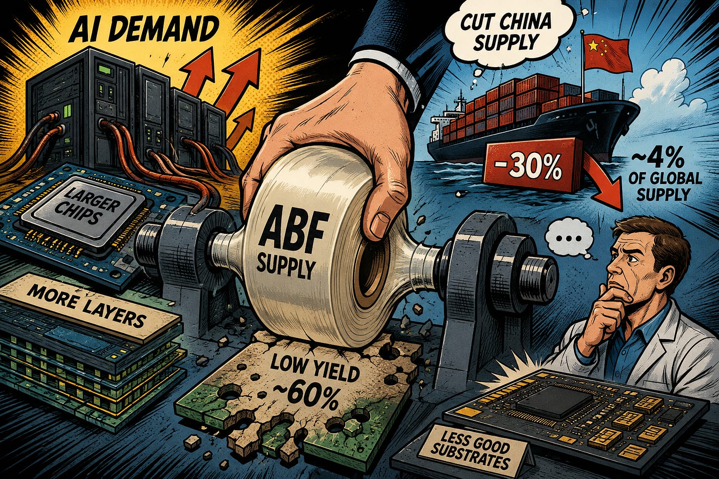
A rumourcirculating through Asia’s semiconductor supply chain has attracted considerable attention. Ajinomoto, the Japanese chemicals group whose build-up film has become an indispensable material for advanced semiconductor substrates, is said to be considering a roughly 30% reduction in shipments to Chinese customers. The idea, according to industry chatter, would be to redirect scarce material towards Japan, Taiwan and other customers serving the booming artificial-intelligence market.
亞洲半導體供應鏈中流傳的一則謠言引發了廣泛關注。據傳,日本化學集團味之素(Ajinomoto)正考慮將其對中國客戶的積層膜出貨量減少約 30%。業界議論指出,此舉旨在將稀缺材料重新導向日本、台灣及其他服務蓬勃發展的人工智慧市場的客戶。
Note: This is only a rumor at this stage and has not been officially announced or confirmed.
註:目前這僅為謠傳,尚未正式宣布或證實。
For substrate makers struggling to secure enough Ajinomoto Build-up Film, or ABF, that sounds encouraging.
對於苦於難以取得足夠味之素積層膜(ABF)的基板製造商而言,這聽起來令人振奮。
The arithmetic is less so.
然而,實際計算結果卻並非如此樂觀。
https://www.linkedin.com/in/jett-c-17972258/recent-activity/images/
Below we will share:以下我們將分享:
China accounts for only around % of global ABF consumption (Taiwan %, Japan **% ), according to industry estimates. Even assuming that the rumoured 30% cut is real—and that every square metre taken away from Chinese customers can immediately be reassigned elsewhere—the amount released would equal only:
根據產業估計,中國僅佔全球 ABF 消費量的約 %(台灣 %,日本 **%)。即使假設傳聞中的 30% 削減屬實,且從中國客戶處收回的每一平方公尺都能立即重新分配給其他地區,所釋出的數量也僅相當於:


8月19日8 月 19 日
China accounts for only around 13% of global ABF consumption (Taiwan 40%, Japan 30% ), according to industry estimates. Even assuming that the rumoured 30% cut is real—and that every square metre taken away from Chinese customers can immediately be reassigned elsewhere—the amount released would equal only:
根據產業估計,中國僅佔全球 ABF 消費量的約 13%(台灣 40%,日本 30%)。即使假設傳聞中的 30% 削減屬實,且從中國客戶處收回的每一平方公尺都能立即重新分配給其他地區,所釋出的數量也僅相當於:
13% × 30% = 3.9% of global consumption.
13% × 30% = 3.9% 的全球消費量。
That may help a few customers at the margin. It will not solve a structural shortage.
這或許能幫助少數邊緣客戶,但無法解決結構性的短缺問題。
The reason is that the ABF problem is no longer simply about how many square metres of film can be produced. AI is changing the economics of semiconductor substrates themselves. Packages are getting larger, build-up structures are becoming more complicated and, crucially, manufacturing yields deteriorate as the substrates become more ambitious.
原因在於,ABF 的問題已不再單純是能夠生產多少平方公尺的薄膜。人工智慧(AI)正在改變半導體基板的經濟結構。封裝尺寸日益增大,堆疊結構愈趨複雜,而關鍵的是,隨著基板設計更具挑戰性,製造良率也隨之下降。
The result is an awkward equation for the industry:
這為產業帶來了一個棘手的等式:
larger substrates × more layers × lower yields = much higher effective ABF consumption.
更大的基板 × 更多的層數 × 更低的良率=有效 ABF 消耗量大幅增加。
That is why reallocating a few percentage points of global supply will probably do little more than buy time.
正因如此,僅重新配置全球供應量的幾個百分點,恐怕頂多只能爭取一些時間。
AI has changed the substrate
AI 改變了基板
ABF has been around for decades. Its role is deceptively mundane: it forms the insulating build-up layers through which increasingly dense copper interconnects are created inside high-end IC substrates.
ABF 已存在數十年。其作用看似平凡:它在高階 IC 基板內部形成絕緣堆疊層,透過這些層可建構日益密集的銅互連結構。
But the substrate beneath a modern AI accelerator bears little resemblance to that underneath an ordinary processor of a decade ago.
但現代 AI 加速器下方的基板,與十年前普通處理器下方的基板已大不相同。
5月14日5 月 14 日
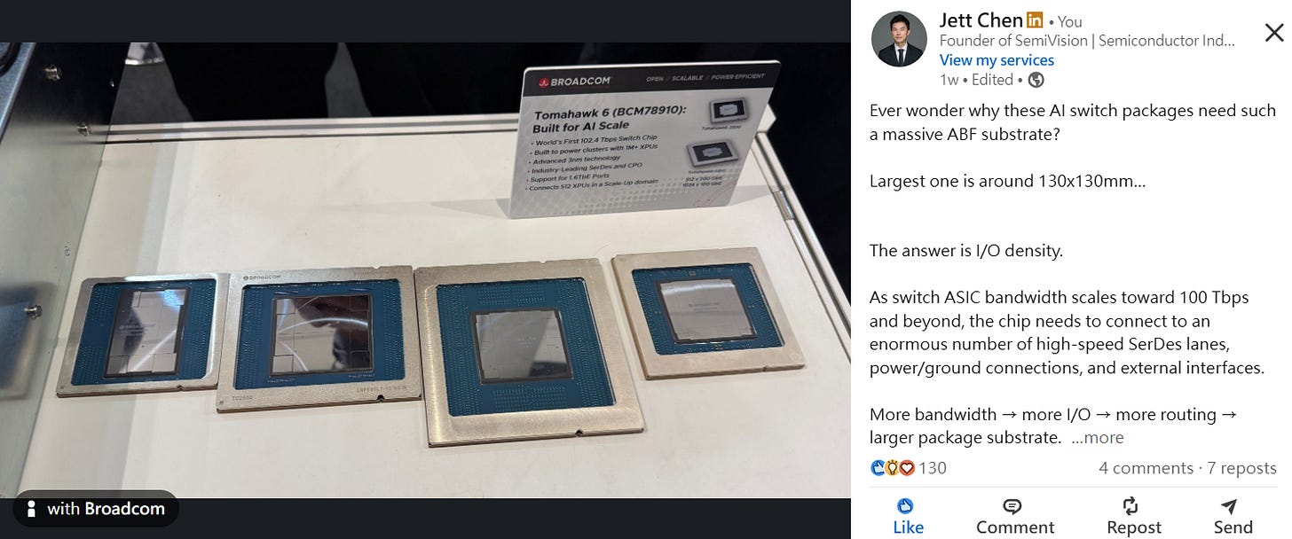
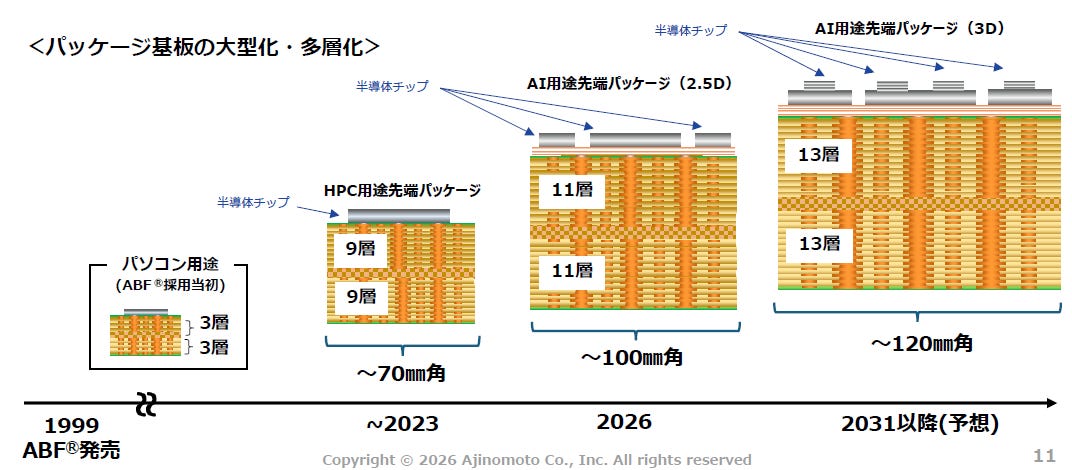
AI GPUs and custom accelerators are becoming enormous. Their packages must connect multiple compute dies, HBM stacks and increasingly complex power and signal networks. The substrate underneath them therefore has to become larger as well.
AI GPU 與客製化加速器正變得日益龐大。其封裝必須連接多個運算晶片、HBM 堆疊,以及愈來愈複雜的電源與訊號網路。因此,位於其下方的基板也必須隨之增大。

Some advanced AI substrates now approach roughly 10cm by 10cm, according to supply-chain discussions. Structures such as 9-2-9—nine build-up layers on either side of a two-layer core—illustrate how far complexity has risen.
根據供應鏈討論,部分先進的 AI 基板尺寸已接近 10 公分乘 10 公分。諸如 9-2-9 的結構(核心兩層,兩側各九層堆疊層)說明了複雜度已提升至何種程度。
For ABF suppliers this matters enormously.
對 ABF 供應商而言,這至關重要。
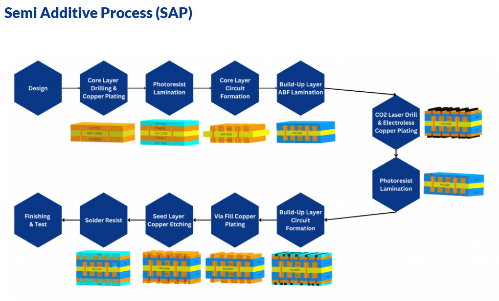
A substrate that doubles in area does not merely need more material once. Every additional build-up layer requires another round of material and processing. Lamination is followed by laser drilling, desmear, copper plating, lithography and patterning. Then the process is repeated.
基板面積增加一倍,並非僅需多使用一次材料。每一層額外的積層都需要再進行一輪材料投入與製程處理。壓合之後,接著是雷射鑽孔、去膠渣、銅電鍍、微影及線路成形。隨後,整個製程再次重複。
The material intensity of an advanced AI substrate is therefore better thought of as:
因此,先進 AI 基板的材料密集度更應理解為:
Substrate area × Number of build-up layers
基板面積 × 積層層數
rather than simply the number of processors shipped.
而非僅僅是出貨的處理器數量。
This distinction is becoming increasingly important as AI accelerators migrate towards larger packages and more elaborate routing architectures.
隨著 AI 加速器朝向更大封裝與更複雜的繞線架構發展,此項區別正變得日益重要。
The broader market is already expanding rapidly. Japan market survey estimates that global sales volume of interlayer dielectric materials will rise from 19m square metres in 2025 to 22.9m in 2026 and 27.5m in 2027. By 2030 it expects demand to reach 41m square metres, implying compound annual growth of nearly 15% between 2024 and 2030.
整體市場已迅速擴張。日本市場調查預估,全球層間介電材料銷售面積將從 2025 年的 1,900 萬平方公尺,增至 2026 年的 2,290 萬平方公尺,並於 2027 年達到 2,750 萬平方公尺。至 2030 年,需求預計將達 4,100 萬平方公尺,意味著 2024 年至 2030 年間的年均複合成長率接近 15%。
That would be brisk growth even without a manufacturing problem.
即使沒有製造問題,這也將是一項強勁的成長。
There is one.有一個。

5月5日5 月 5 日
The yield trap良率陷阱
For some of the largest 9-2-9 substrates, supply-chain estimates suggest manufacturing yields may currently be only around 60%. The figure varies considerably by product, design, line width and spacing, via architecture and substrate maker; it should therefore not be treated as an industry-wide benchmark.
針對部分最大的 9-2-9 基板,供應鏈預估目前的製造良率可能僅約 60%。此數據會因產品、設計、線寬與間距、通孔架構以及基板製造商而有顯著差異;因此,不應將其視為全產業的基準。
But as an illustration, 60% is revealing.
但作為說明,60% 這個數字已足以揭示問題。
If a manufacturer needs to deliver 100 good substrates at a final yield of 60%, it must begin with the equivalent of roughly:
若製造商需以 60% 的最終良率交付 100 片合格基板,則必須從相當於約:
100 ÷ 0.60 = 167 units.
100 ÷ 0.60 = 167 單位的數量開始生產。
In other words, for every 100 good substrates shipped, the factory may have to absorb the manufacturing cost of roughly 67 additional units.
換言之,每出貨 100 片合格基板,工廠可能必須吸收額外約 67 單位的製造成本。
From the perspective of usable output, the material requirement has effectively been multiplied by1.67 times.
從可用產出的角度來看,材料需求實際上已增加為原本的 1.67 倍。
And even that calculation understates the problem.
而且,這樣的估算甚至還低估了問題的嚴重性。
Substrates are manufactured sequentially. A defect discovered near the beginning of the process wastes relatively little value. A failure discovered after several build-up layers have already been laminated, drilled and plated destroys not only the substrate but all the ABF and processing capacity already consumed.
基板的製造是依序進行的。若在製程初期發現缺陷,所浪費的價值相對較少;但若在已經完成多層堆疊、壓合、鑽孔與電鍍後才發現故障,則不僅基板報廢,連帶已消耗的 ABF 材料與所有投入的製程產能也都付諸流水。
Yield therefore matters not merely because bad substrates are thrown away. What matters is where in the process they become bad.
因此,良率的重要性不僅在於不良基板會被報廢,更關鍵的是它們在製程中的哪個階段變為不良品。
Source: QDOS來源:QDOS
A defect on the eighth build-up layer is far more expensive than a defect on the first.
第八層堆疊層的缺陷成本遠高於第一層。
This is one reason the semiconductor materials market can tighten much faster than forecasts based purely on final chip shipments would suggest.
這也是半導體材料市場緊縮速度可能遠快於僅依據最終晶片出貨量預測的原因之一。
Four per cent meets 40 per cent
百分之四滿足百分之四十
Now return to the rumoured Chinese allocation cut.
現在回到傳聞中對中國的配額削減。
Even if Ajinomoto could free up something close to 4% of global supply, the demand environment against which that incremental volume must be measured is expanding much faster.
即使味之素能釋出接近全球供應量 4% 的產能,但必須衡量此增量產能的市場需求環境,其擴張速度遠為更快。
Ajinomoto’s recent semiconductor-market presentation cites WSTS forecasts suggesting the logic-IC market could grow by roughly 37% in 2026 and another 27% in 2027, driven largely by AI-related demand.
味之素近期在半導體市場的簡報中引用 WSTS 的預測,指出邏輯 IC 市場在人工智慧相關需求的強力帶動下,2026 年有望成長約 37%,2027 年則再增 27%。
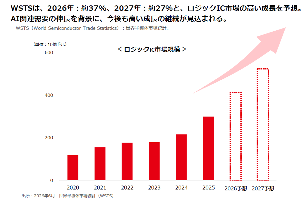
Compounded, that would imply a market approximately 74% larger after two years:
若以複利計算,這意味著兩年後市場規模將擴大約 74%:
1.37 × 1.27 ≈ 1.74.
1.37 × 1.27 ≈ 1.74。
Logic-chip revenue and ABF consumption obviously do not move one-for-one. Yet the fastest-growing segment of logic happens to be precisely the one using some of the largest, most complicated and most ABF-intensive substrates.
邏輯晶片營收與 ABF 消耗量顯然並非呈一比一變動。然而,成長最快速的邏輯晶片區塊,恰恰是使用最大、最複雜且最耗費 ABF 之基板者。
A 4% redistribution of supply is therefore being asked to offset a much larger structural increase in consumption.
因此,要求僅 4% 的供應重新分配來抵銷遠為龐大的結構性消費增長,實屬不可能。
It cannot.這辦不到。
The wrong way to measure capacity
衡量產能的錯誤方式
This leads to a broader problem with the way investors often analyse the ABF market.
這導致投資者分析 ABF 市場時常面臨一個更廣泛的問題。
Nominal capacity is usually expressed in square metres.
名義產能通常以平方公尺表示。
That is useful but increasingly insufficient.
這雖然有用,但已日益不足。
What matters to an AI-substrate customer is not simply whether a supplier can manufacture one million additional square metres of dielectric film. It matters whether that material has the right coefficient of thermal expansion, dielectric properties, surface characteristics, adhesion, laser-processability and reliability for a large, high-layer-count substrate.
對 AI 基板客戶而言,關鍵不在於供應商能否多生產一百萬平方公尺的介電薄膜,而在於該材料是否具備適合大型、高層數基板的熱膨脹係數、介電特性、表面特性、附著力、雷射加工性與可靠性。
Then it must be qualified by the customer.
接著,該材料必須通過客戶認證。
Then the substrate maker must be able to manufacture with it at an acceptable yield.
然後,基板製造商必須能夠以可接受的良率使用該材料進行生產。
Only after all three conditions have been met does nominal capacity become effective capacity.
唯有在上述三項條件全部達成後,名目產能才能轉化為有效產能。
The distinction helps explain why alternative suppliers cannot immediately eliminate Ajinomoto’s bottleneck.
此區別有助於解釋為何替代供應商無法立即消除 Ajinomoto 的瓶頸。
Ajinomoto Fine-Techno remains the de facto standard in the market. Japan market survey also lists suppliers including Sekisui Chemical and Taiwan’s WaferChem Technology among participants in interlayer dielectric materials.
Ajinomoto Fine-Techno 仍是市場上的實際標準。日本市場調查亦列出包括 Sekisui Chemical 與台灣的 WaferChem Technology 在內的供應商,參與層間介電材料的供應。
The existence of alternatives is important. But qualification in semiconductor packaging is slow, particularly when the product involved sits beneath GPUs costing tens of thousands of dollars.
替代方案的存在至關重要。然而,在半導體封裝領域的認證流程緩慢,尤其是當相關產品位於價值數萬美元的 GPU 下方時。
No hyperscaler wants to discover that a cheaper dielectric film saves a few dollars on the substrate while reducing the reliability of an AI accelerator worth orders of magnitude more.
沒有任何超大型雲端服務業者願意發現,為了在基板上節省幾美元而採用較便宜的介電薄膜,卻導致價值高出數個數量級的 AI 加速器可靠性下降。
Ajinomoto is expanding. AI is expanding faster.
Ajinomoto 正在擴張,但 AI 的擴張速度更快。
Ajinomoto itself clearly recognises the problem.
Ajinomoto 本身顯然已認知到這個問題。
Its recent materials show manufacturing centred around Kawasaki and Gunma, with the Gunma site serving as an important volume-production base. The company has also announced the acquisition of land for another manufacturing site in Gifu.
其近期資料顯示,生產重心位於川崎與群馬,其中群馬廠區作為重要的量產基地。該公司亦已宣布在岐阜收購土地,以設立另一處生產據點。
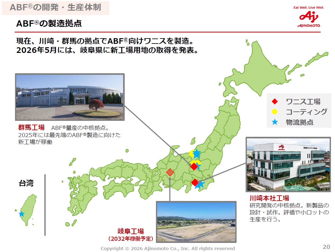

That is significant. But building chemical-material capacity, installing equipment, qualifying production and obtaining customer approval takes years.
這確實至關重要。然而,建立化學材料產能、安裝設備、完成生產認證並取得客戶核准,往往需要耗時數年。
AI demand does not intend to wait.
AI 的需求不會等待。
This creates a potentially uncomfortable period in which advanced substrate demand rises faster than fully qualified ABF capacity.
這將造成一段潛在的艱難時期,先進基板的需求增長速度快於完全合格的 ABF 產能。
And it explains why the industry’s response will probably involve more than Ajinomoto building another factory.
這也解釋了為何產業的回應可能不僅限於味之素(Ajinomoto)增建另一座工廠。
Substrate makers will try to raise yields. Customers will qualify second sources. Material companies will develop lower-CTE and lower-loss alternatives. Some package architectures may themselves evolve to reduce dependence on conventional organic substrates.
基板製造商將致力提升良率;客戶將認證第二貨源;材料公司將開發更低熱膨脹係數(CTE)與更低損耗的替代方案;部分封裝架構本身也可能演進,以降低對傳統有機基板的依賴。
None of these solutions is instantaneous.
這些解決方案均無法立即見效。
The real bottleneck真正的瓶頸
The most interesting implication of the current shortage is therefore not whether China receives 30% less Ajinomoto film.
因此,當前短缺最有趣的影響,並非中國是否少收到 30% 的味之素積層膜。
That is a redistribution question.
這是一個重新分配的問題。
The more consequential issue is how quickly the industry can increase the amount of qualified material that becomes good substrate.
更關鍵的議題在於,產業能以多快的速度提升可轉化為合格基板的材料產量。
For the next generation of AI packages, analysts should therefore watch three metrics rather than one:
針對下一代 AI 封裝,分析師應關注三項指標,而非僅一項:
High-end qualified ABF capacity, substrate layer count and final manufacturing yield.
高階合格 ABF 產能、基板層數與最終製程良率。
These variables increasingly determine how much material the industry actually needs.
這些變數日益決定產業實際所需的材料數量。
If a 10cm-by-10cm 9-2-9 substrate genuinely achieves only around 60% yield during early production, the difference between nominal demand and effective material consumption becomes enormous.
若一塊 10 公分乘 10 公分的 9-2-9 基板在初期生產階段的實際良率僅約 60%,則名義需求與有效材料消耗之間的差距將極為巨大。
That is the uncomfortable lesson behind the latest ABF shortage.
這正是最新一波 ABF 短缺背後令人不安的教訓。
Cutting Chinese allocation by 30% might release roughly 4% of worldwide supply. But the AI industry is simultaneously building larger substrates, adding more layers and wasting more material before each good unit reaches the customer.
將中國的配額削減 30%,或許僅能釋出約 4% 的全球供應量。然而,AI 產業同時正致力於打造更大的基板、增加更多層數,導致在每一顆良品送達客戶之前,材料損耗也隨之增加。
The semiconductor industry has spent the past few years worrying about shortages of GPUs and HBM.
過去幾年,半導體產業一直擔憂 GPU 與 HBM 的短缺問題。
The next bottleneck may look considerably less glamorous.
下一個瓶頸可能看起來遠沒那麼光鮮。
It comes on a roll of insulating film.
它以絕緣薄膜的捲狀形式供應。

5月4日5 月 4 日
The yield trap良率陷阱
ABF substrate yield also depends heavily on circuit complexity.
ABF 基板的良率也高度依賴電路的複雜度。
The roughly 60% yield mentioned earlier is closer to a relatively simple design. For advanced AI or CPO substrates around 10cm × 10cm, supply-chain feedback suggests yields can fall below 50%. Larger and more complex substrates may be closer to 40%.
前述約 60% 的良率較接近相對簡單的設計。針對先進 AI 或 CPO 基板(尺寸約 10cm × 10cm),供應鏈反饋顯示良率可能降至 50% 以下;更大且更複雜的基板,良率則可能接近 40%。
That changes material consumption dramatically:
這會大幅改變材料消耗量:
60% yield →1.67×input per good substrate
60% 良率 → 每片合格基板需 1.67 倍投入
50% yield →2.0×50% 良率 → 2.0 倍
40% yield →2.5×40% 良率 → 2.5 倍
And much of the scrap has already consumed multiple ABF layers and expensive processing steps.
而且許多廢料已經消耗了多層 ABF 薄膜以及昂貴的製程步驟。
So the real ABF demand equation is increasingly:
因此,真正的 ABF 需求公式正日益變為:
Area × Layers × Design Complexity ÷ Yield
面積 × 層數 × 設計複雜度 ÷ 良率
This is why a small reallocation of ABF supply cannot solve the shortage. Poor yield itself is becoming a major source of material consumption.
這正是為何僅小幅重新配置 ABF 供應無法解決缺貨問題。不良的良率本身已成為材料消耗的主要來源。
Thanks for reading SEMIVISION @_@! This post is public so feel free to share it.
感謝閱讀 SEMIVISION @_@!本文為公開文章,歡迎自由分享。


Share分享
Previous上一頁