Taiwan’s AI “Five Tigers”: The Full-Stack Supply Chain to Watch at SEMICON Taiwan 2026
Taiwan’s AI “Five Tigers”: The Full-Stack Supply Chain to Watch at SEMICON Taiwan 2026
- Source: SemiVision
- Author: SEMIVISION
- Published: 2026-08-19T10:46:29+08:00
- URL: https://tspasemiconductor.substack.com/p/taiwans-ai-five-tigers-from-silicon
中文翻譯與英文原文(雙語)
(1) 台灣 AI「五虎將」:2026 年 SEMICON Taiwan 值得關注的全棧供應鏈 --- (1) Taiwan’s AI “Five Tigers”: The Full-Stack Supply Chain to Watch at SEMICON Taiwan 2026


Taiwan’s AI “Five Tigers”: From Silicon to Servers, the Supply Chain Behind AI
台灣 AI「五虎」:從矽晶到伺服器,背後的 AI 供應鏈
Original Article By SemiVision Research [Reading time: 11 mins]
原文作者:SemiVision Research [閱讀時間:11 分鐘]

Aug 19, 2026
Share分享
Taiwan’s AI “Five Tigers”: From Silicon to Servers, the Supply Chain Behind AI
台灣 AI「五虎」:從矽晶到伺服器,背後的 AI 供應鏈
Source: SEMI來源:SEMI
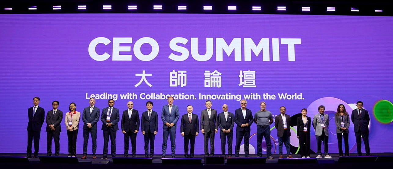
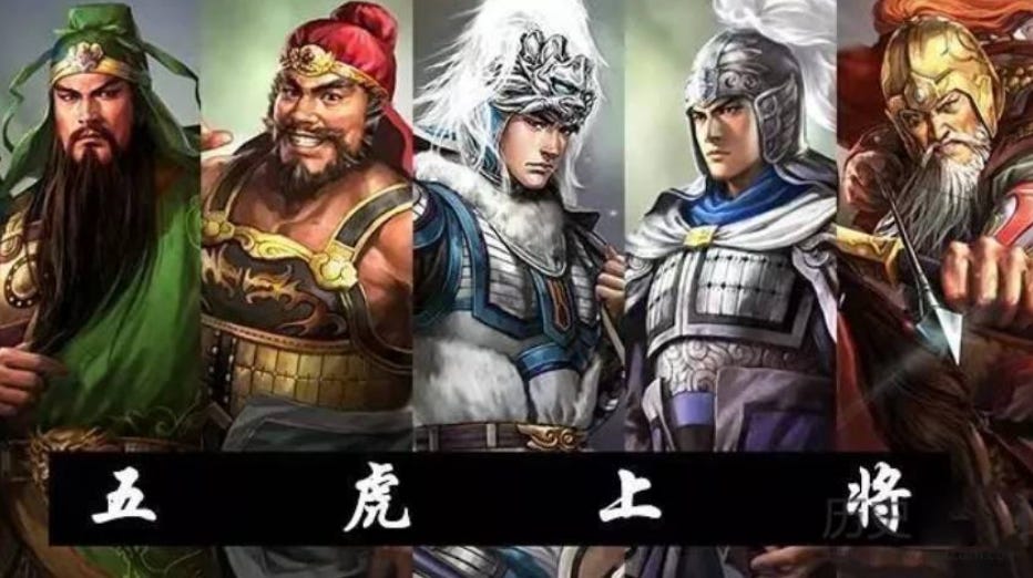
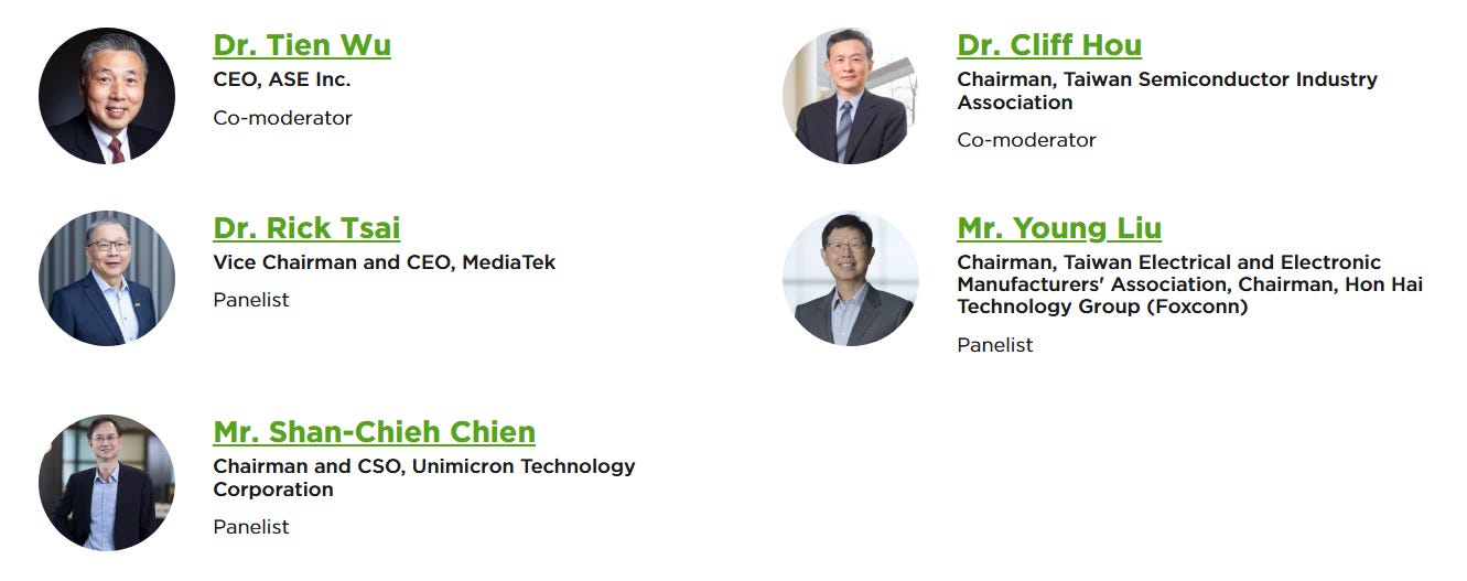
SEMICON Taiwan 2026will feature an unusual lineup: TSMC, ASE, MediaTek, Unimicron, and Hon Hai/Foxconn appearing together in the same discussion. Taiwanese media has labeled them the semiconductor industry’s“Five Tigers.” The term is not an official industry classification, but the analogy is useful. In Chinese history and popular culture, the “Five Tiger Generals” referred to five leading commanders who fought on different fronts but collectively formed the military core of the same camp. Taiwan’s five companies play a similar role in AI infrastructure: they are not direct competitors, but each controls a different and increasingly critical layer of the hardware stack.
SEMICON Taiwan 2026 將呈現罕見的陣容:台積電、日月光、聯發科、欣興電子與鴻海/富士康共同參與同一場討論。台灣媒體將它們稱為半導體產業的「五虎」。此稱呼並非正式的產業分類,但此一類比頗具參考價值。在中國歷史與流行文化中,「五虎上將」指的是五位在不同戰線作戰、卻共同構成同一陣營軍事核心的頂尖將領。台灣的這五家企業在 AI 基礎設施中扮演類似角色:它們並非直接競爭對手,但各自掌握硬體堆疊中不同且日益關鍵的層級。
MediaTek represents AI ASIC design, TSMC advanced logic manufacturing, ASE advanced packaging and test, Unimicron high-end ABF substrates and PCBs, while Foxconn sits at the system level, integrating processors, networking, power, cooling, and mechanical infrastructure into deployable AI servers and racks. Viewed together, the five companies provide a useful framework for understanding why Taiwan’s position in AI is much broader than wafer fabrication alone.
聯發科代表 AI ASIC 設計,台積電負責先進邏輯製程製造,日月光專注於先進封裝與測試,欣興電子提供高階 ABF 載板與印刷電路板(PCB),而鴻海則立足於系統層級,將處理器、網路、電源、散熱及機械基礎設施整合為可部署的 AI 伺服器與機櫃。綜觀這五家企業,它們提供了一個實用的框架,有助於理解為何台灣在 AI 領域的地位遠不止於晶圓製造 alone。
That distinction matters because the AI infrastructure race is no longer simply about who can secure the most GPUs. The bottlenecks are migrating across the stack, from HBM and advanced packaging to substrates, optical connectivity, power delivery, liquid cooling, rack integration, and eventually the construction of entire data centers. The competitive unit is gradually moving from the chip to the package, from the package to the rack, and from the rack to the AI factory. That is the backdrop against which these “Five Tigers” should be analyzed.
此區別至關重要,因為 AI 基礎設施的競賽已不再單純取決於誰能取得最多的 GPU。瓶頸正沿著技術堆疊向上游移動,從 HBM 與先進封裝,延伸至基板、光學互連、電源供應、液冷散熱、機櫃整合,乃至最終整個資料中心的建置。競爭單位正逐漸從晶片轉向封裝,從封裝轉向機櫃,再從機櫃邁向 AI 工廠。這正是分析「五大虎」的背景脈絡。

8月17日8 月 17 日
SEMIVISION @_@ 是一份由讀者支持的出版物。若要接收最新文章並支持我的工作,歡迎考慮成為免費或付費訂閱者。
MediaTek: From Mobile SoCs to AI Infrastructure Silicon
聯發科:從行動 SoC 邁向 AI 基礎設施矽元件
MediaTek is still primarily associated with smartphone SoCs, but that description is becoming increasingly incomplete. The more strategically important part of the company’s roadmap is its expansion into AI data-center ASICs, where hyperscalers are looking for alternatives to a purely merchant-GPU architecture. These customers are not necessarily trying to replace NVIDIA across every workload. Instead, they are developing custom silicon for workloads where they can improve cost, power efficiency, memory architecture, networking, or software control relative to a general-purpose accelerator.
聯發科仍主要被視為智慧型手機 SoC 供應商,但此描述已日益不足。該公司路線圖中更具戰略意義的部分,是其進軍 AI 資料中心專用積體電路(ASIC)領域;在此領域,超大型雲端服務業者正尋求純商用 GPU 架構之外的替代方案。這些客戶未必意圖在所有工作負載上全面取代 NVIDIA,而是針對特定工作負載開發客製化晶片,以期在成本、電源效率、記憶體架構、網路連線或軟體控制等方面,相較於通用加速器獲得更佳表現。
This creates a very different opportunity from the traditional mobile semiconductor market. Building a competitive AI ASIC requires much more than RTL design. It requires access to leading-edge process technology, advanced SerDes, HBM integration, chiplets, advanced packaging, and increasingly close coordination with system-level power and networking architectures. MediaTek has accumulated many of these capabilities through years of designing complex mobile and connectivity SoCs, making its move into data-center silicon more credible than it might initially appear.
這創造了與傳統行動半導體市場截然不同的機會。打造具競爭力的 AI ASIC 所需的不僅是 RTL 設計,更須取得先進製程技術、高速 SerDes、HBM 整合、Chiplet 技術、先進封裝能力,並需與系統層級的電源及網路架構進行日益緊密的協同作業。聯發科透過多年設計複雜的行動與連網 SoC,已累積上述多項關鍵能力,使其進軍資料中心晶片的佈局,較表面看來更為可信。
The key question for investors is not whether custom ASICs will replace GPUs. NVIDIA’s ecosystem remains extraordinarily difficult to displace because its advantage extends well beyond silicon into CUDA, networking, rack-scale architecture, and software. The more relevant question is how much incremental AI compute will migrate toward custom accelerators developed by Google, Amazon, Meta, Microsoft, and other hyperscalers. Even if GPUs remain dominant, a relatively modest shift in incremental workloads toward custom silicon could create a very large addressable market for MediaTek and Taiwan’s broader ASIC ecosystem.
對投資人而言,關鍵問題不在於客製化 ASIC 是否將取代 GPU。NVIDIA 的生態系極難被撼動,因為其優勢遠超越矽晶本身,延伸至 CUDA、網路技術、機架級架構以及軟體層面。更值得探討的問題是,有多少新增的 AI 運算需求將轉向由 Google、Amazon、Meta、Microsoft 及其他超大型雲端業者所開發的客製化加速器。即便 GPU 仍居主導地位,只要新增工作負載中有相對小幅的比例移往客製化矽晶,就足以為聯發科及台灣更廣泛的 ASIC 生態系創造龐大的潛在市場。
This is why MediaTek deserves more attention at SEMICON Taiwan. The company is increasingly moving from a mobile-chip narrative toward an infrastructure-silicon narrative. If this transition succeeds, it could become one of the more important structural changes in Taiwan’s semiconductor landscape over the next several years.
這正是聯發科在 SEMICON Taiwan 值得更多關注的原因。該公司正逐漸從行動晶片的故事線,轉向基礎設施矽晶的新敘事。若此轉型成功,將成為未來數年台灣半導體產業版圖中最重要的結構性變革之一。
2025年7月15日2025 年 7 月 15 日

2025年6月28日2025 年 6 月 28 日
TSMC: The Foundry Is Becoming a System Platform
台積電:晶圓代工廠正轉型為系統平台
TSMC’s importance to AI is obvious, but the nature of that importance is changing. The conventional description of TSMC as a semiconductor foundry is becoming too narrow because modern AI accelerators depend not only on leading-edge transistors, but also on HBM integration, silicon interposers, redistribution layers, advanced bonding, chiplets, and increasingly complex packaging architectures.
台積電對人工智慧的重要性顯而易見,但其重要性的本質正在發生變化。將台積電單純描述為半導體晶圓代工廠已顯得過於狹隘,因為現代 AI 加速器不僅依賴最先進的電晶體,還取決於 HBM 整合、矽中介層、重分佈層、先進接合技術、小晶片(Chiplets),以及日益複雜的封裝架構。
The result is that the manufacturing problem is expanding from wafer fabrication into system integration. CoWoS is the most visible example. During the early phase of the generative-AI boom, GPU availability was often described as the central constraint. That quickly shifted to HBM, then to CoWoS, and now the bottleneck is becoming more distributed across interposers, substrates, thermal design, test capacity, optical connectivity, and package yield.
其結果是,製造挑戰已從晶圓製程擴展至系統整合。CoWoS 即是最顯著的例子。在生成式 AI 興起的初期階段,GPU 供貨常被視為主要瓶頸;隨後迅速轉為 HBM,接著是 CoWoS 產能;如今,瓶頸已更廣泛地分散於中介層、基板、散熱設計、測試產能、光學互連以及封裝良率等環節。
This changes what TSMC is effectively selling. A next-generation AI accelerator is less like a conventional monolithic semiconductor and more like a miniature computing system assembled within a package. As compute dies, I/O dies, HBM stacks, interposers, and eventually optical engines are integrated more tightly, advanced packaging becomes part of processor architecture rather than a downstream manufacturing step.
這改變了台積電實際銷售的產品本質。新一代 AI 加速器已不像傳統的單晶半導體,更像是在封裝內組裝而成的微型運算系統。隨著運算晶片、I/O 晶片、HBM 堆疊、中介層乃至光學引擎的整合日益緊密,先進封裝已成為處理器架構的一部分,而非下游的製造步驟。
For that reason, the most important question at SEMICON Taiwan is no longer simply how much additional CoWoS capacity TSMC plans to add. The more fundamental issue is how large and complex an AI package can become before existing manufacturing architectures encounter physical or economic limits. The answer will determine demand for new bonding tools, inspection systems, substrate materials, thermal interfaces, panel-level packaging, and potentially optical I/O. In other words, TSMC’s evolution is increasingly pushing the industry toward what can be described as system foundry economics.
正因如此,SEMICON Taiwan 最關鍵的問題已不再單純是台積電計劃增加多少 CoWoS 產能。更根本的議題在於,在現有製造架構遭遇物理或經濟極限之前,AI 封裝的尺寸與複雜度能達到何種程度。答案將決定對新型接合設備、檢測系統、基板材料、熱介面材料、面板級封裝以及潛在光學 I/O 的需求。換言之,台積電的演進正日益推動產業邁向可稱為「系統晶圓代工經濟」的模式。

7月13日7 月 13 日
5月14日5 月 14 日

7月14日7 月 14 日
ASE: Advanced Packaging Moves Back Into the Critical Path
ASE:先進封裝重新成為關鍵路徑
AI has also changed the strategic position of OSAT companies. Historically, much of the semiconductor industry’s value creation was perceived to sit toward the front end: design the chip, fabricate the wafer, and then send it downstream for packaging and testing. That hierarchy is becoming less accurate because packaging is now one of the primary determinants of how much compute, memory, and I/O can be integrated into a usable AI system.
人工智慧也改變了 OSAT 廠商的戰略地位。過去,半導體產業的價值創造被認為主要集中在前端:設計晶片、製造晶圓,然後送至後段進行封裝與測試。然而,這種層級觀念已逐漸失準,因為封裝現已成為決定可實際運作的 AI 系統中能整合多少運算能力、記憶體容量及 I/O 頻寬的主要因素之一。
This makes advanced packaging part of processor architecture. ASE’s VIPack platform, for example, spans advanced redistribution, fan-out, 2.5D and 3D integration, and heterogeneous chiplet architectures. The strategic value of these technologies increases as AI packages grow larger and more complex, because package size directly affects yield, warpage, thermal behavior, routing density, and assembly economics.
這使得先進封裝成為處理器架構的一部分。以日月光(ASE)的 VIPack 平台為例,其涵蓋先進重佈層、扇出型、2.5D 與 3D 整合,以及異質性小晶片(chiplet)架構。隨著 AI 封裝尺寸日益增大且更為複雜,這些技術的戰略價值也隨之提升,因為封裝尺寸直接影響良率、翹曲、熱行為、佈線密度及組裝經濟效益。
Panel-level packaging is particularly interesting in this context. Wafer-level processes work extremely well when package dimensions remain relatively small, but AI accelerators are moving in the opposite direction. More compute dies, more HBM stacks, more I/O, and larger interposers all increase the pressure to process larger rectangular areas more efficiently. At some point, the economics of fabricating very large packages on circular wafers becomes increasingly uncomfortable, which is one reason panel-level approaches continue to attract attention.
在此背景下,面板級封裝(Panel-level packaging)尤為引人注目。當封裝尺寸相對較小時,晶圓級製程表現極為出色;然而,AI 加速器的发展趨勢卻恰恰相反。更多的運算晶片(compute dies)、更多的高頻寬記憶體(HBM)堆疊、更多的輸入/輸出(I/O),以及更大的中介層(interposers),都增加了對更高效處理大面積矩形區域的壓力。在某個臨界點之後,在圓形晶圓上製造超大尺寸封裝的經濟效益將變得日益不理想,這也是面板級方法持續受到關注的原因之一。
For ASE, the strategic question is therefore not simply how much advanced packaging TSMC may outsource. The more important issue is whether ASE can develop architectures and manufacturing platforms that are complementary to, rather than merely downstream from, TSMC’s packaging roadmap. If that happens, the role of OSAT could move from manufacturing support back into the critical path of AI system development.
因此,對日月光(ASE)而言,戰略問題不僅在於台積電(TSMC)可能外包多少先進封裝產能。更關鍵的議題是,日月光能否開發出與台積電封裝路線圖互補、而非僅處於其下游的架構與製造平台。若能做到這一點,封測代工廠(OSAT)的角色便有可能從單純的製造支援,重新回歸到 AI 系統開發的關鍵路徑上。

2025年6月18日2025 年 6 月 18 日
Unimicron: The Substrate Is Becoming a Bottleneck
欣興電子:基板正成為瓶頸
ABF substrates are easy to underestimate because they appear passive compared with GPUs, HBM, or advanced packaging. In reality, larger AI accelerators are turning the substrate into an increasingly difficult engineering problem. As more compute dies and HBM stacks are integrated into a single package, the substrate must support higher routing density, more I/O, greater layer counts, tighter line-and-space requirements, and increasingly severe mechanical and thermal stresses.
ABF 基板容易被低估,因為與 GPU、HBM 或先進封裝相比,它們看似被動元件。事實上,隨著 AI 加速器尺寸不斷增大,基板已成為日益嚴峻的工程挑戰。當更多運算晶粒與 HBM 堆疊整合至單一封裝時,基板必須支援更高的佈線密度、更多的 I/O 數量、更多的層數、更嚴格的線寬/線距要求,以及日益嚴苛的機械與熱應力。
Package growth is especially important. Larger substrates make warpage harder to control, while higher-speed electrical interfaces tighten signal-integrity requirements. At the same time, more layers, more vias, and larger panel areas reduce manufacturing margin for error. These effects compound one another, meaning that the substrate can become a limiting factor even when silicon and HBM are available.
封裝成長尤為關鍵。基板尺寸越大,翹曲越難控制;而更高速的電氣介面則對訊號完整性提出更嚴格的要求。同時,層數增加、通孔數量增多以及面板面積擴大,均會壓縮製造容錯空間。這些效應相互疊加,意味著即使矽晶圓與 HBM 供貨無虞,基板仍可能成為制約因素。
This is why the most useful question for Unimicron is not simply whether ABF pricing will rise. The more important issue is how large next-generation AI substrates need to become and what material systems can support that scaling. Once package dimensions move higher, the implications extend well beyond substrate makers themselves. Demand shifts upstream into low-loss glass cloth, ABF films, copper foil, specialty resin systems, drilling and laser equipment, plating, inspection, and potentially glass-core substrates.
這就是為什麼對欣興電子而言,最有價值的問題並非僅止於 ABF 價格是否上漲。更關鍵的議題在於,下一代 AI 基板需要達到多大的尺寸,以及何種材料系統能夠支撐此種擴展。一旦封裝尺寸向上提升,其影響將遠超出基板製造商本身。需求將向上游轉移至低損耗玻璃布、ABF 薄膜、銅箔、特殊樹脂系統、鑽孔與雷射設備、電鍍、檢測,乃至玻璃核心基板。
The substrate should therefore be viewed as part of the same scaling problem as advanced packaging. Both are responding to the fact that AI processors are becoming physically larger, electrically denser, and mechanically more difficult to manufacture. If the next generation of accelerator packages pushes substrate dimensions substantially higher, this area could become one of the most important bottlenecks in the supply chain.
因此,基板應被視為與先進封裝同一個擴展難題的一部分。兩者皆需應對 AI 處理器在物理尺寸上日益增大、電氣密度更高、且機械製造難度更嚴峻的事實。若下一代加速器封裝推動基板尺寸大幅成長,此領域可能成為供應鏈中最關鍵的瓶頸之一。

2025年6月30日2025 年 6 月 30 日

2025年6月9日2025 年 6 月 9 日
Foxconn: From Server Assembly to AI Factory Integration
鴻海:從伺服器組裝到 AI 工廠整合
The first four Tigers can produce world-class semiconductor components, but none of them alone creates usable AI infrastructure. Someone still has to integrate GPUs, CPUs, switches, power systems, cooling hardware, cables, NICs, trays, racks, and management systems into a platform that can operate reliably inside a data center. This is where Foxconn becomes strategically important.
前四隻老虎雖能生產世界級的半導體元件,但單靠任何一家都無法打造可用的 AI 基礎設施。仍須有人將 GPU、CPU、交換器、電源系統、散熱硬體、纜線、網卡(NIC)、托盤、機架及管理系統,整合為能在資料中心內穩定運作的平台。這正是鴻海具備戰略重要性的關鍵所在。
The company is increasingly difficult to describe as simply an electronics manufacturing services provider. AI servers are changing the nature of the product being manufactured. The unit of deployment is moving away from an individual server toward the rack, while the rack itself is becoming a tightly integrated computing system involving power distribution, liquid cooling, high-speed networking, mechanical design, and increasingly complex system validation.
該公司已愈來愈難以被單純定義為電子製造服務(EMS)供應商。AI 伺服器正改變所製造產品的本質,部署單位已從單一伺服器轉向機櫃層級;而機櫃本身也演變為高度整合的運算系統,涵蓋電源分配、液冷散熱、高速網路、機構設計,以及日益複雜的系統驗證。
This is particularly important as NVIDIA moves from standalone GPU platforms toward rack-scale architectures. Blackwell accelerated this transition, and Rubin is likely to push it further. The challenge for ODMs is no longer simply to assemble a motherboard inside a chassis; it is to coordinate a complete system in which power, thermals, networking, and compute architecture all constrain one another.
隨著 NVIDIA 從獨立 GPU 平台轉向機架級架構,這一點變得尤為重要。Blackwell 加速了此一轉型,而 Rubin 很可能會進一步推動此趨勢。對 ODM 廠商而言,挑戰已不再只是將主機板組裝於機殼內,而是要協調一個完整的系統,其中電力、散熱、網路與運算架構彼此相互制約。
The strategic question is therefore whether companies such as Foxconn remain primarily manufacturing partners or evolve into infrastructure integrators capable of delivering increasingly complete AI factories. If customers begin procuring not only servers or racks but megawatt-scale computing blocks, the value captured by system integrators could rise materially. In that scenario, Foxconn’s role would move further upstream in system design and further downstream into data-center deployment at the same time.
因此,戰略性問題在於:像鴻海(Foxconn)這樣的企業,是繼續主要扮演製造夥伴的角色,還是演進為能夠交付日益完整 AI 工廠的基礎設施整合者?若客戶開始採購的不僅是伺服器或機架,而是兆瓦級的運算模組,系統整合者所創造的價值可能會顯著提升。在這種情境下,鴻海的角色將同時更向上游延伸至系統設計,並更向下游拓展至資料中心部署。

6月11日6 月 11 日

5月29日5 月 29 日
What to Watch at SEMICON Taiwan 2026
2026 年 SEMICON Taiwan 展會焦點
The most interesting part of SEMICON Taiwan this year may not be any single new piece of equipment. The more important signals are likely to come from how different parts of the AI supply chain are beginning to constrain one another.
今年 SEMICON Taiwan 最引人入勝之處,或許並非任何單一的新型設備。更重要的訊號,可能來自人工智慧供應鏈各環節開始相互制約的方式。
The first issue is the speed at which custom ASIC demand is growing. GPUs will remain central to AI infrastructure, but hyperscaler silicon programs are multiplying, and that trend benefits not only design houses such as MediaTek but also foundries, HBM suppliers, substrate vendors, advanced packaging companies, and test-equipment makers. Custom ASIC does not need to displace NVIDIA to become one of the semiconductor industry’s largest growth markets.
首要議題在於客製化 ASIC 需求的成長速度。GPU 仍將是 AI 基礎設施的核心,但超大型資料中心業者的晶片計畫正快速增加,此趨勢不僅利於聯發科等設計公司,也惠及晶圓代工廠、HBM 供應商、基板廠商、先進封測企業以及測試設備製造商。客製化 ASIC 無需取代 NVIDIA,即可成為半導體產業成長最快速的市場之一。
The second issue is whether advanced packaging remains the industry’s dominant scaling constraint. The semiconductor industry has responded to slowing monolithic scaling by integrating more compute and memory at the package level, but this does not eliminate bottlenecks; it moves them. HBM, interposers, bonding, substrates, package yield, thermal management, and test capacity are increasingly interconnected. The manufacturing chain is no longer linear, because limitations in one layer can quickly propagate across the entire system.
第二個問題在於,先進封裝是否仍是產業擴張的主要瓶頸。面對單晶製程微縮放緩,半導體產業已轉向在封裝層級整合更多運算與記憶體資源,然而此舉並未消除瓶頸,僅是將其轉移。高頻寬記憶體(HBM)、中介層、鍵合技術、基板、封裝良率、熱管理以及測試產能等環節日益緊密交織。製造鏈已不再呈線性發展,因為任一層面的限制都可能迅速擴散至整個系統。
The third issue is package size. Larger packages offer more routing resources, more memory bandwidth, and more compute integration, but they also worsen warpage, thermal stress, substrate complexity, and yield. This is why technologies such as larger interposers, panel-level packaging, glass substrates, hybrid bonding, and optical I/O deserve attention. Much of the next AI hardware cycle may be determined by how effectively the industry can continue increasing package scale without allowing manufacturing economics to deteriorate too rapidly.
第三個議題是封裝尺寸。較大的封裝能提供更多佈線資源、更高的記憶體頻寬以及更強的運算整合能力,但同時也會加劇翹曲、熱應力、基板複雜度並影響良率。這正是為何較大尺寸的中介層、面板級封裝、玻璃基板、混合鍵結與光學 I/O 等技術值得關注。下一波 AI 硬體週期的發展,很大程度上將取決於產業能否在持續擴大封裝規模的同時,避免製造經濟效益過快惡化。
A fourth question is whether the product itself is becoming the rack. The semiconductor industry historically optimized chips, then moved toward optimizing packages, and is now increasingly optimizing entire rack-scale systems. Compute, networking, memory, optics, power, and cooling have to be co-designed, creating opportunities far beyond semiconductor vendors. Power companies, liquid-cooling suppliers, connector makers, cable vendors, rack builders, and system integrators are becoming increasingly strategic participants in the AI infrastructure stack.
第四個問題是:產品本身是否正逐漸演變為機櫃?半導體產業過去著重於晶片優化,隨後轉向封裝優化,如今則日益聚焦於整個機櫃等級系統的優化。運算、網路、記憶體、光學、電源與散熱必須進行協同設計,這為半導體供應商以外的領域創造了龐大商機。電力公司、液冷解決方案供應商、連接器製造商、線纜廠商、機櫃組裝廠以及系統整合商,正成為人工智慧基礎設施架構中愈來愈具戰略意義的參與者。
The final question, and arguably the most valuable one for investors, is where the next bottleneck will emerge. AI has already created extreme tightness in HBM and CoWoS, and it is putting pressure on high-end PCB materials, advanced substrates, copper foil, glass cloth, power systems, and optical components. The largest opportunities often appear when an item previously treated as a low-value component suddenly becomes capacity-constrained or technologically difficult. SEMICON Taiwan is therefore useful not merely as a showcase of existing winners, but as a place to identify the next part of the system that is becoming physically difficult to build.
最後一個問題,也是對投資人而言最具價值的一項,在於下一個瓶頸將出現在何處。人工智慧已造成高頻寬記憶體(HBM)與 CoWoS 先進封裝產能極度緊繃,同時也对高階印刷電路板材料、先進基板、銅箔、玻璃布、電源系統及光學元件帶來壓力。最大的投資機會往往出現在某個過去被視為低價值零組件的項目,突然面臨產能限制或技術挑戰之際。因此,SEMICON Taiwan 不僅是展示現有贏家的舞台,更是識別系統中下一項在實體製造上日益困難之關鍵環節的重要場合。

6月18日6 月 18 日
Taiwan’s Real AI Moat Is Industrial Density
台灣的真正 AI 護城河在於產業密度
The biggest mistake investors can make is to analyze Taiwan’s AI advantage company by company. TSMC is critical, but TSMC alone does not explain Taiwan. Neither do MediaTek, ASE, Unimicron, or Foxconn individually. The deeper advantage is the density of the industrial ecosystem and the speed at which different layers of that ecosystem can interact.
投資者可能犯下的最大錯誤,就是逐家公司分析台灣的 AI 優勢。台積電固然至關重要,但單靠台積電並不足以解釋台灣的全貌;同樣地,聯發科、日月光、欣興電子或鴻海各自也無法單獨說明這一點。更深层的優勢在於產業生態系的密度,以及該生態系不同層級之間互動的速度。
Within a relatively small geographic area, Taiwan contains semiconductor design houses, leading-edge foundries, OSATs, substrate makers, PCB suppliers, ODMs, power-electronics companies, cooling suppliers, connector vendors, test-equipment companies, specialty chemical producers, and precision manufacturing firms. That concentration materially reduces engineering iteration time. When an accelerator requires a larger substrate, substrate vendors can work directly with material suppliers. When warpage becomes a problem, packaging houses, equipment makers, and chemical suppliers can adjust processes in parallel. When rack power rises toward hundreds of kilowatts, server ODMs can redesign with power and cooling companies rather than treating those systems as downstream components.
在相對狹小的地理範圍內,台灣匯聚了半導體設計公司、先進製程晶圓代工廠、OSAT 廠商、基板製造商、PCB 供應商、ODM 業者、電力電子公司、散熱供應商、連接器供應商、測試設備公司、特殊化學品生產商以及精密製造廠商。這種產業聚落顯著縮短了工程迭代的時間。當加速器需要更大尺寸的基板時,基板供應商可直接與材料供應商協作;當翹曲成為問題時,封測廠、設備製造商與化學品供應商可同步調整製程;當機架功耗攀升至數百千瓦等級時,伺服器 ODM 業者可與電力及散熱公司共同重新設計,而非將這些系統視為下游零組件處理。
The advantage is therefore not simply lower manufacturing cost. It is engineering velocity.
因此,其優勢不僅在於較低的製造成本,更在於工程推進速度。
This is why the “Five Tigers” framework is useful. MediaTek, TSMC, ASE, Unimicron, and Foxconn are not five versions of the same company. They represent five layers of the same AI infrastructure machine. As AI moves from chip-level competition toward system-level optimization, the value of that coordination increases.
這正是「五虎」架構的價值所在。聯發科、台積電、日月光、欣興電子與鴻海並非同一家公司的五種變體,而是代表同一套 AI 基礎設施機器的五個層級。隨著人工智慧從晶片層級的競爭轉向系統層級的優化,這種協同效應的價值將日益提升。
For investors attending SEMICON Taiwan 2026, the objective should therefore not simply be to identify the next fashionable semiconductor technology. The more valuable exercise is to understand where AI systems are becoming physically difficult, expensive, or capacity-constrained to build. Wherever complexity rises fastest, the next bottleneck—and often the next major supply-chain opportunity—is usually not far behind.
對於參與 SEMICON Taiwan 2026 的投資人而言,目標不應僅是識別下一項熱門的半導體技術。更具價值的做法,是釐清 AI 系統在哪些環節面臨實體建構上的困難、成本高昂或產能受限。凡複雜度攀升最快之處,下一個瓶頸——往往也是下一個重大的供應鏈商機——通常就在不遠處。

2025年9月16日2025 年 9 月 16 日
SEMIVISION @_@ 是一份由讀者支持的出版物。若要接收最新文章並支持我的工作,歡迎考慮成為免費或付費訂閱者。


Share分享
Previous上一頁