TSMC × Sony vs. China’s Rising CIS Ecosystem: The Next Front in Semiconductor Competition
TSMC × Sony vs. China’s Rising CIS Ecosystem: The Next Front in Semiconductor Competition
- Source: SemiVision
- Author: SEMIVISION
- Published: 2026-08-13T09:50:05+08:00
- URL: https://tspasemiconductor.substack.com/p/tsmc-sony-vs-chinas-rising-cis-ecosystem
中文翻譯與英文原文(雙語)
台積電 × 索尼 vs. 中國崛起的 CIS 生態系:半導體競爭的下一個前線 --- TSMC × Sony vs. China’s Rising CIS Ecosystem: The Next Front in Semiconductor Competition


TSMC × Sony vs. China’s Rising CIS Ecosystem: The Next Front in Semiconductor Competition
台積電 × 索尼 vs. 中國崛起的 CIS 生態系:半導體競爭的下一個前線
Original Article By SemiVision Research [Reading time: 11 mins]
原文作者:SemiVision Research [閱讀時間:11 分鐘]

Aug 13, 2026
Share分享
TSMC × Sony vs. China’s Rising CIS Ecosystem: The Next Front in Semiconductor Competition
台積電 × 索尼 vs. 中國崛起的 CIS 生態系:半導體競爭的下一個前線
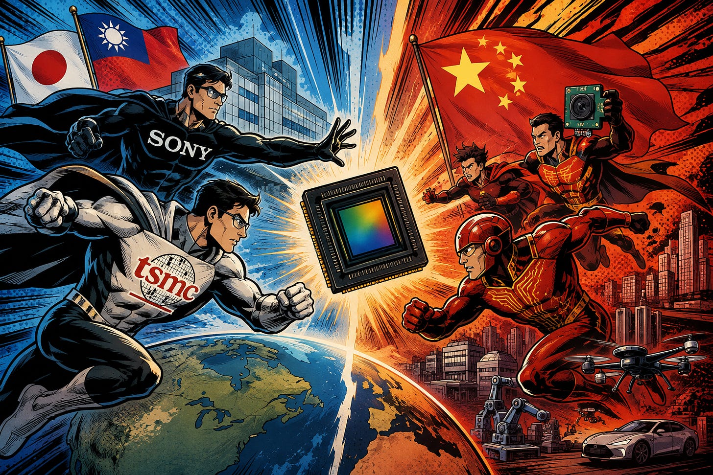
While almost every semiconductor discussion in 2026 has been dominated by AI GPUs, HBM, advanced packaging and data-center infrastructure, another strategically important semiconductor battle is moving rapidly into the foreground: the image sensor.
儘管 2026 年幾乎所有的半導體討論都聚焦於 AI GPU、HBM、先進封裝與資料中心基礎設施,另一場具戰略重要性的半導體戰役正迅速浮上檯面:影像感測器。
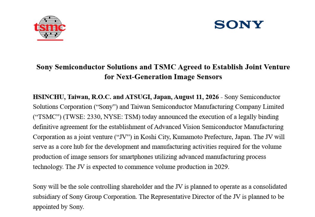
On August 11, Sony Semiconductor Solutions and TSMC signed a legally binding definitive agreement to establish Advanced Vision Semiconductor Manufacturing Corporation in Koshi City, Kumamoto Prefecture. The joint venture is scheduled to begin volume production in 2029 and will become a core development and manufacturing hub for next-generation smartphone image sensors using advanced process technologies.
8 月 11 日,Sony Semiconductor Solutions 與台積電簽署具有法律約束力的最終協議,將於熊本縣合志市成立「先進視覺半導體製造公司」(Advanced Vision Semiconductor Manufacturing Corporation)。該合資企業預計於 2029 年開始量產,並將成為採用先進製程技術開發與製造下一代智慧型手機影像感測器的核心基地。
Sony will remain the controlling shareholder and lead core sensor technology development, product planning and design. Sony plans to contribute approximately ¥465 billion, including cash and assets from its newly built Koshi fab, while TSMC plans to contribute approximately ¥282 billion in cash. The investments will be phased according to demand and business conditions.
Sony 將保持控股股東地位,並主導核心感測器技術開發、產品規劃與設計。Sony 計劃出資約 4,650 億日圓,包含現金及其新建合志晶圓廠的資產;台積電則計劃以現金出資約 2,820 億日圓。相關投資將依據市場需求與業務狀況分階段進行。
This is therefore much more than another foundry agreement.
因此,這不僅僅是另一項晶圓代工協議。
It represents a structural change in how the image-sensor industry may operate during the next decade.
這代表影像感測器產業在未來十年的運作模式將發生結構性變革。
Sony brings arguably the world’s strongest image-sensor product definition, pixel architecture and customer understanding. TSMC brings advanced logic processes, manufacturing discipline, yield management and a production ecosystem capable of translating increasingly complex semiconductor architectures into high-volume products.
Sony 擁有堪稱全球最頂尖的影像感測器產品定義、像素架構與客戶洞察力;台積電則提供先進的邏輯製程、嚴謹的製造管理、良率控制能力,以及能將日益複雜的半導體架構轉化為量產產品的完整生產生態系。
Together, they are effectively creating a new industrial model for imaging:
雙方攜手,正共同打造一種全新的影像產業新模式:
sensor innovation led by the application company, logic manufacturing enabled by the world’s leading foundry, and production geographically anchored inside a strategically supported Japanese semiconductor cluster.
由應用端企業主導感測器創新,由全球領先的晶圓代工廠賦能邏輯製造,並將生產基地紮根於獲戰略支持的日本半導體聚落之中。
And behind the deal is an even larger story.
而這項交易背後,蘊藏著更為宏大的局勢。
The global CIS industry is beginning to split into competing—and sometimes overlapping—technology ecosystems centered on Japan, Taiwan, China and U.S.-controlled computing platforms.
全球 CIS 產業正逐漸分裂為以日本、台灣、中國及美國主導的運算平台為核心的競爭性技術生態系,且這些生態系有時彼此重疊。
2025年9月4日2025 年 9 月 4 日
SEMIVISION @_@ 是一份由讀者支持的出版物。若要接收最新文章並支持我的工作,歡迎考慮成為免費或付費訂閱者。
Image Sensors Are Becoming Computing Devices
影像感測器正轉型為運算裝置
Traditionally, CMOS image-sensor competition was relatively straightforward.
傳統上,CMOS 影像感測器的競爭相對單純。
The industry competed on pixel size, resolution, sensitivity, dynamic range, low-light performance, power consumption and manufacturing cost.
產業競爭焦點集中在畫素尺寸、解析度、靈敏度、動態範圍、低光源表現、功耗以及製造成本。
That model is changing.然而,此模式正在發生改變。
A smartphone camera is no longer simply capturing an image and sending it to an application processor. Modern imaging systems increasingly combine multiple exposures, multiple cameras, depth information, motion sensing and machine-learning algorithms before the user even sees the final image.
智慧型手機相機已不再只是單純捕捉影像並傳送給應用處理器。現代影像系統在用戶看到最終影像之前,便已整合多重曝光、多鏡頭協同運作、深度資訊、動態感測以及機器學習演算法。
The next step is even more important.
下一步更為關鍵。
As AI moves from cloud-based language models toward on-device AI, robotics, autonomous vehicles, industrial machines and spatial computing, the sensor itself becomes part of the computing architecture.
隨著人工智慧從基於雲端的語言模型轉向裝置端 AI、機器人技術、自動駕駛車輛、工業機器及空間運算,感測器本身已成為運算架構的一部分。
The camera is becoming the front-end processor of the physical world.
相機正逐漸成為實體世界的前端處理器。
That requires increasingly sophisticated stacked architectures: a highly optimized pixel layer for photon capture combined with increasingly capable logic underneath it for readout, signal processing, memory management and potentially AI acceleration.
這需要日益精進的堆疊式架構:高度優化的像素層用於捕捉光子,並結合其下方功能更強大的邏輯層,負責訊號讀取、訊號處理、記憶體管理,以及潛在的 AI 加速。
Sony has already pushed aggressively into stacked CIS architectures. TSMC’s participation suggests that the distinction between a traditional CMOS sensor and an advanced heterogeneous computing device will continue to blur.
Sony 已積極投入堆疊式 CIS 架構的開發。台積電的參與顯示,傳統 CMOS 感測器與先進異質運算裝置之間的界線將持續模糊。
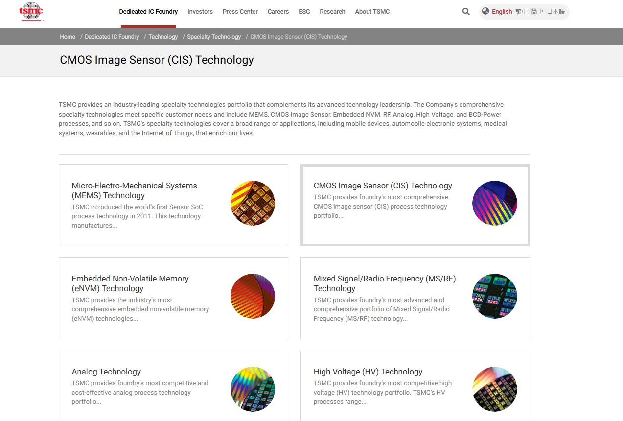
The manufacturing requirements begin to resemble some of the challenges appearing elsewhere in advanced semiconductors: finer interconnects, more complex wafer stacking, higher bandwidth between functional layers, increasingly sophisticated bonding and tighter co-optimization between design and manufacturing.
製造需求開始呈現出與先進半導體其他領域相似的挑戰:更精細的互連、更複雜的晶圓堆疊、功能層之間更高的頻寬、日益精密的接合技術,以及設計與製造之間更緊密的共同優化。
In other words, advanced packaging concepts are gradually entering the imaging world as well.
換言之,先進封裝概念也逐漸進入影像領域。
Why Kumamoto Matters為何熊本至關重要
The location may be almost as important as the technology.
地點的重要性幾乎不亞於技術本身。
Kumamoto has already become the symbolic center of Japan’s semiconductor revival through TSMC’s JASM investments. Sony’s existing image-sensor manufacturing footprint makes the region even more strategically significant.
透過台積電 JASM 的投資,熊本已成為日本半導體復興的象徵中心。而索尼既有的影像感測器製造佈局,更讓該區域具備極高的戰略意義。
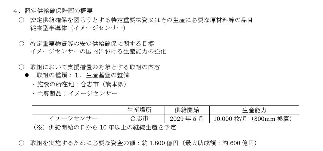
Japan’s Ministry of Economy, Trade and Industry had already approved Sony’s Koshi image-sensor project under Japan’s economic-security framework in April 2026. The approved plan targeted approximately 10,000 300mm-equivalent wafers per month, with supply beginning around May 2029 and production expected to continue for at least ten years. METI said subsidies could reach ¥60 billion.
日本經濟產業省已於 2026 年 4 月依據日本經濟安全框架,核准索尼位於菊陽的影像感測器專案。該核准計畫目標為每月產能約相當於 1 萬片 300 毫米晶圓,預計自 2029 年 5 月起開始供貨,生產期至少持續十年。經產省表示,補貼金額最高可達 600 億日圓。
This makes the policy intention unusually clear.
這使得政策意圖異常明確。
Japan does not view image sensors merely as consumer-electronics components. METI explicitly described them as the electronic eyes required for autonomous driving and physical AI.
日本並不將影像感測器僅視為消費性電子元件。日本經濟產業省(METI)明確將其描述為自動駕駛與實體人工智慧所需的「電子之眼」。
The strategy therefore stretches far beyond smartphones.
因此,這項戰略的影響範圍遠超越智慧手機領域。
Japan is assembling a semiconductor ecosystem that combines logic manufacturing, sensors, materials, equipment, automotive electronics and eventually physical-AI applications.
日本正致力於建構一個整合邏輯晶片製造、感測器、材料、設備、車用電子,並最終延伸至實體 AI 應用的半導體生態系。
The Sony-TSMC joint venture turns Kumamoto from simply another wafer-production location into something closer to an integrated semiconductor technology cluster.
Sony 與台積電的合資企業,將熊本從單純的晶圓生產基地,轉型為更接近整合型半導體技術聚落的樞紐。
And the timing matters.而時機至關重要。
On the same day the Sony partnership was finalized, TSMC’s board approved another US$29.4425 billion capital budget covering advanced process capacity, advanced packaging, mature and specialty technologies, fabs and infrastructure. The board also formally approved investment of up to ¥282 billion in the Sony joint venture.
在與索尼合作案拍板定案的同日,台積電董事會通過了另一筆高達 294.425 億美元的資本預算,涵蓋先進製程產能、先進封裝、成熟與特殊製程技術,以及晶圓廠和基礎設施。董事會也正式核准對索尼合資企業投資最高達 2,820 億日圓。
Seen in that context, image sensors are not a side project.
在此脈絡下,影像感測器絕非邊緣專案。
They are becoming another extension of TSMC’s manufacturing platform.
它們正逐漸成為台積電製造平台的另一項延伸。

8月4日8 月 4 日
Supply-Chain Observation #1: The Opportunity Moves Beyond the Sensor Die
供應鏈觀察 #1:機會已超越感測器晶粒本身
The first-order beneficiaries are obvious: Sony and TSMC.
首要受益者顯而易見:Sony 與台積電。
But the more interesting opportunities may appear one or two layers further down the supply chain.
但更值得關注的機會,可能出現在供應鏈往下游的一至兩層。
A more sophisticated stacked image sensor requires significantly more than front-end wafer fabrication.
更先進的堆疊式影像感測器所需的不僅是前段晶圓製程。
It creates demand for technologies associated with:
這將帶動對以下技術的需求:
wafer-to-wafer bonding, hybrid bonding, wafer thinning, temporary bonding and debonding, backside processing, CMP, advanced lithography, precision metrology, wafer inspection, dicing, test and highly controlled contamination management.
晶圓對晶圓接合、混合接合、晶圓薄化、臨時接合與解接合、背側製程、化學機械拋光(CMP)、先進微影、精密量測、晶圓檢測、切割、測試,以及高度嚴格的污染管控。
Japan is particularly well positioned here because its semiconductor strength is unusually concentrated in materials, manufacturing equipment and precision processing technologies.
日本在此領域特別具備優勢,因為其半導體產業實力異常集中於材料、製造設備與精密加工技術。
Companies across photoresists, silicon wafers, CMP materials, bonding materials, inspection, deposition, cleaning, dicing and test could therefore participate indirectly as the Kumamoto ecosystem expands.
隨著熊本生態系的擴張,涵蓋光阻、矽晶圓、CMP 材料、接合材料、檢測、沉積、清洗、切割與測試等領域的企業,亦將間接參與其中。

6月16日6 月 16 日
But one distinction is important for investors: not every supplier in the Japanese semiconductor ecosystem automatically becomes a beneficiary.
但有一項區別對投資人至關重要:並非日本半導體生態系中的每家供應商都能自動成為受益者。
The key questions will be which process steps Sony and TSMC internalize, which tools are qualified for the new architecture and whether critical packaging or stacking operations remain in Japan or are distributed across existing Sony and TSMC facilities.
關鍵問題在於:Sony 與台積電將內部化哪些製程步驟、哪些設備已通過新架構的認證,以及關鍵的封裝或堆疊作業是留在日本,還是分散至現有的 Sony 與台積電廠區進行。
Those qualification announcements may ultimately be more useful investment signals than the headline fab announcement itself.
這些認證公告最終可能比晶圓廠設立的頭條新聞更具投資參考價值。
Supply-Chain Observation #2: Smartphone Camera Competition Is Becoming a Manufacturing Battle
供應鏈觀察#2:智慧型手機相機競爭正演變為製造之戰
Sony’s biggest immediate battlefield remains premium smartphones.
Sony 目前最大的戰場仍是高階智慧型手機。
Yole Group estimated that Sony represented close to 50% of global CIS revenue in 2025, with its position supported by premium mobile imaging, larger optical formats and advanced stacked architectures. In mobile specifically, Yole estimated Sony’s share at approximately 57%.
Yole Group 估計,2025 年 Sony 佔全球 CIS 營收近 50%,其地位受惠於高階行動影像、更大光學格式及先進堆疊式架構。特別是在行動領域,Yole 估計 Sony 的市佔率約為 57%。
That explains why the partnership matters strategically.
這也說明了此合作夥伴關係在戰略上的重要性。
As flagship smartphones become increasingly homogeneous in CPU performance, displays and memory, camera capability remains one of the clearest ways manufacturers can differentiate devices to consumers.
隨著旗艦智慧型手機在 CPU 效能、顯示器與記憶體方面日趨同質化,相機功能仍是製造商向消費者區隔產品最明確的方式之一。
But the camera competition is shifting.
但相機競賽的格局正在轉變。
Future differentiation may come not simply from larger sensors or more megapixels, but from tighter integration between the sensor, ISP, application processor and AI software.
未來的差異化可能不再僅來自更大的感測器或更高的畫素數,而是取決於感測器、影像訊號處理器(ISP)、應用處理器與 AI 軟體之間更緊密的整合。
That favors suppliers capable of coordinating multiple layers of semiconductor technology simultaneously.
這有利於能夠同時協調多層半導體技術的供應商。
Sony plus TSMC therefore creates a formidable combination.
因此,Sony 與 TSMC 的結合形成了強大的聯盟。
The consequence will propagate through the smartphone imaging ecosystem: camera-module makers, lens suppliers, autofocus and stabilization components, packaging providers, testing companies and optical-material suppliers will all face increasingly demanding specifications.
其影響將擴及智慧型手機影像生態系:相機模組製造商、鏡頭供應商、自動對焦與防手震元件廠商、封裝服務提供商、測試公司以及光學材料供應商,都將面臨日益嚴苛的規格要求。
Supply-Chain Observation #3: China Is No Longer Just Competing at the Low End
供應鏈觀察 #3:中國不再僅限於低階市場競爭
This is where the geopolitical story becomes much more interesting.
這正是地緣政治故事變得更加引人入勝之處。
For years, the simplified industry narrative was that Sony dominated premium sensors, Samsung challenged Sony in smartphones, while Chinese CIS companies competed primarily through price and domestic substitution.
多年來,產業界的簡化敘事認為:Sony 主宰高階感測器市場,Samsung 在智慧型手機領域挑戰 Sony,而中國 CIS 廠商則主要透過價格競爭與國產替代來爭取市占。
That description is becoming outdated.
這樣的描述已逐漸過時。
According to industry analysis, China became the world’s second-largest CIS supplier base in 2025, overtaking South Korea, driven by companies including OmniVision, SmartSens, GalaxyCore and Gpixel.
根據產業分析,2025 年中國已超越南韓,成為全球第二大 CIS 供應商基地,背後推手包括 OmniVision、SmartSens、GalaxyCore 與 Gpixel 等企業。
This is a major structural development.
這是一項重大的結構性發展。
Chinese CIS companies are benefiting from one of the world’s largest domestic ecosystems for smartphones, surveillance systems, EVs, drones, robotics, AIoT devices and smart-home products.
中國 CIS 廠商正受益於全球最大的國內生態系統之一,涵蓋智慧手機、監控系統、電動車、無人機、機器人、AIoT 裝置及智慧家庭產品。
That means China possesses something extraordinarily valuable for semiconductor development:
這意味著中國擁有對半導體發展極為珍貴的資源:
A massive internal application market capable of generating both volume and rapid product iteration.
一個龐大的內部應用市場,能夠同時創造規模效應並加速產品迭代。
The competitive challenge is therefore not simply whether Chinese companies can reproduce an existing Sony sensor.
因此,真正的競爭挑戰不在於中國企業能否複製現有的 Sony 感測器。
The bigger question is whether Chinese sensor suppliers can use China’s enormous downstream electronics ecosystem to shorten the feedback loop between sensor design, systems integration and commercialization.
更關鍵的問題在於,中國的感測器供應商能否利用中國龐大的下游電子生態系統,縮短從感測器設計、系統整合到商業化之間的回饋循環。
That is exactly how semiconductor ecosystems become dangerous competitors.
這正是半導體生態系統成為危險競爭對手的方式。
Leica × Gpixel Is a Signal the Industry Should Not Ignore
徠卡 × 長光辰芯:產業界不應忽視的信號
One transaction illustrates this shift particularly well.
有一筆交易特別能說明此趨勢。
On April 20, 2026, German premium camera manufacturer Leica Camera AG announced a strategic partnership with China’s Gpixel to jointly develop a high-performance CMOS sensor specifically tailored for future Leica cameras.
2026 年 4 月 20 日,德國頂級相機製造商 Leica Camera AG 宣布與中國的 Gpixel 建立策略合作夥伴關係,共同開發專為未來 Leica 相機量身打造的高效能 CMOS 感測器。
This is not simply an off-the-shelf component procurement agreement.
這並非單純的現成元件採購協議。
Leica and Gpixel said they will cooperate on sensor engineering, validation, image tuning and production readiness, with engineering resources spanning Wetzlar, Antwerp and Changchun.
徠卡與長光辰芯表示,雙方將在感測器工程、驗證、影像調校及量產準備方面展開合作,工程資源將涵蓋德國韋茨拉爾、比利時安特衛普及中國長春。
That matters.這一點至關重要。
Leica is one of the strongest premium imaging brands in the world. A company operating at that level choosing to co-develop a bespoke sensor with a Chinese CIS supplier is an indication that Chinese image-sensor companies are beginning to compete for technology credibility, not merely volume.
徠卡是全球最頂尖的頂級影像品牌之一。如此層級的公司選擇與中國 CIS 供應商共同開發客製化感測器,顯示中國影像感測器廠商正開始爭取技術可信度,而不僅是追求出貨量。
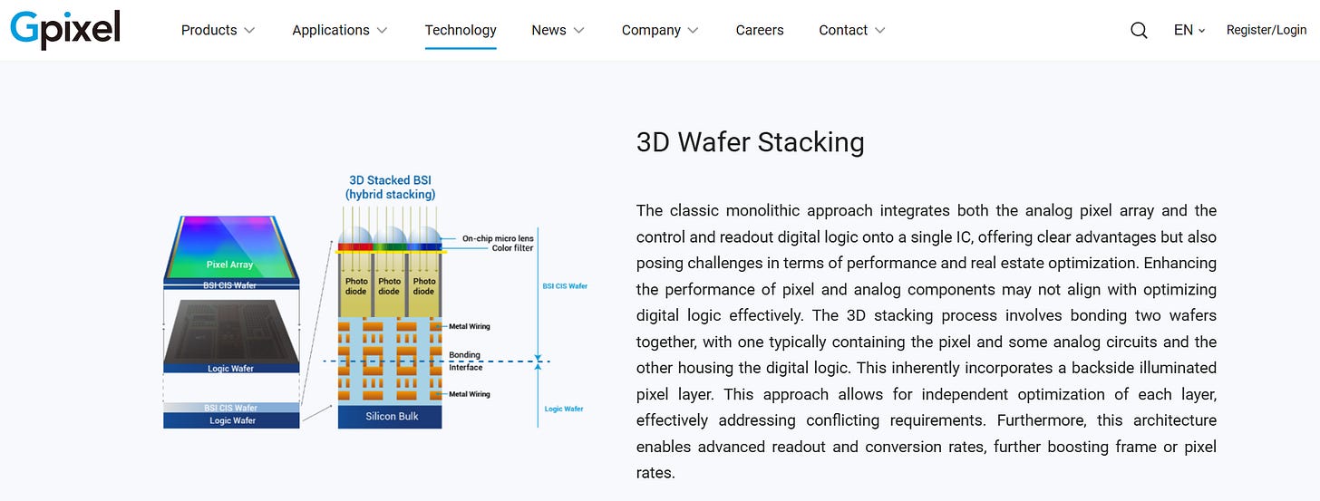
Gpixel’s historical strength has been in industrial, scientific and professional imaging rather than mass-market smartphones. That may actually make the Leica partnership more strategically interesting because advanced industrial imaging requires expertise in areas such as high dynamic range, low noise, high-speed readout and specialized sensor architectures.
長光辰芯過往的優勢在於工業、科學及專業影像領域,而非大眾市場的智慧型手機。這反而使此次與徠卡的合作更具戰略意義,因為先進的工業影像需要在高動態範圍、低雜訊、高速讀取及專用感測器架構等領域具備深厚專業知識。
The Sony-TSMC and Leica-Gpixel announcements therefore form an interesting pair.
因此,索尼與台積電、徠卡與長光辰芯的宣布,構成了一組饒富趣味的對照。
One strengthens a Japan-Taiwan advanced manufacturing alliance.
此舉強化了日台先進製造聯盟。
The other demonstrates that a Chinese CIS supplier can penetrate a premium European imaging platform.
另一項案例證明,中國 CIS 供應商已能打入歐洲高階影像平台。
The global imaging supply chain is not simply decoupling.
全球影像供應鏈並非單純脫鉤,
It is reorganizing into multiple centers of technical competence.
而是重組為多個技術能力中心。
The U.S.-China Competition Is Moving Down the AI Stack
美中競爭正沿著 AI 堆疊向下延伸
The U.S. angle is different.
美國的角度則有所不同。
America does not currently dominate merchant CMOS image sensors in the same way it dominates GPUs or certain parts of semiconductor equipment and EDA.
目前,美國並未像在 GPU 或某些半導體設備與 EDA 領域那樣,主導商用 CMOS 影像感測器市場。
Instead, U.S. influence sits primarily at thesystem and computing-platform layers.
相反,美國的影響力主要集中在系統與運算平台層級。
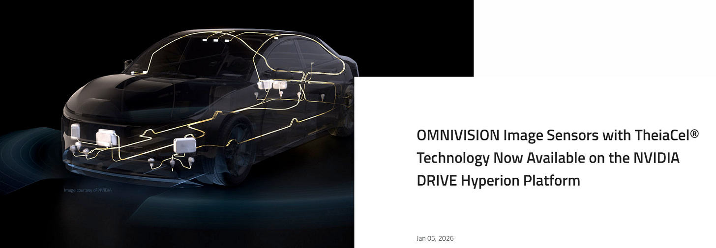
Apple is one of the major drivers of premium mobile imaging demand. NVIDIA increasingly defines computing architectures for autonomous vehicles and robotics. For example, OmniVision’s automotive sensors are already supported on NVIDIA’s DRIVE AGX Hyperion platform.
Apple 是推動高階行動影像需求的主要力量之一。NVIDIA 則日益主導自動駕駛車輛與機器人的運算架構。例如,OmniVision 的車用感測器已支援 NVIDIA 的 DRIVE AGX Hyperion 平台。
At the same time, U.S. semiconductor export policy continues to restrict China’s access to selected advanced computing technologies and semiconductor-manufacturing capabilities, even though CMOS image sensors themselves are not currently treated exactly like leading AI accelerators. BIS continues to maintain dedicated controls around advanced computing and semiconductor-manufacturing items, while its 2026 policy revisions show that access to powerful processors remains explicitly conditioned by national-security considerations.
與此同時,美國半導體出口政策持續限制中國取得選定的先進運算技術與半導體製造能力,儘管 CMOS 影像感測器本身目前並未完全比照頂尖 AI 加速器進行管制。美國工業與安全局(BIS)持續針對先進運算及半導體製造項目實施專項管制,而其 2026 年政策修訂顯示,取得高效能處理器仍明確取決於國家安全考量。
This creates an important strategic consequence.
這帶來了重要的戰略後果。
As restrictions make it harder for China to compete at certain parts of the leading-edge AI compute stack, Beijing and Chinese industry have even stronger incentives to build technological strength in areas where domestic markets can support scale.
隨著限制措施使中國在先進人工智慧運算堆疊的某些環節更難競爭,北京與中國產業界更有強烈動機去發展那些能憑藉國內市場支撐規模效應的技術領域。
Sensors are one of those areas.
感測器即是其中之一。
Automotive semiconductors are another.
車用半導體則是另一項重點領域。
Power electronics, robotics, industrial control and mature-node analog chips are others.
其他領域還包括功率電子、機器人、工業控制以及成熟製程節點的類比晶片。
The future U.S.-China semiconductor competition may therefore become much broader than a race over GPUs.
因此,未來的美中半導體競爭可能遠比 GPU 之爭更為廣泛。
It may become a race to control the entire physical-AI value chain:
這可能演變為對整個實體 AI 價值鏈的控制權爭奪:
Sensor → connectivity → memory → compute → software → actuator.
感測器 → 連線 → 記憶體 → 運算 → 軟體 → 致動器。
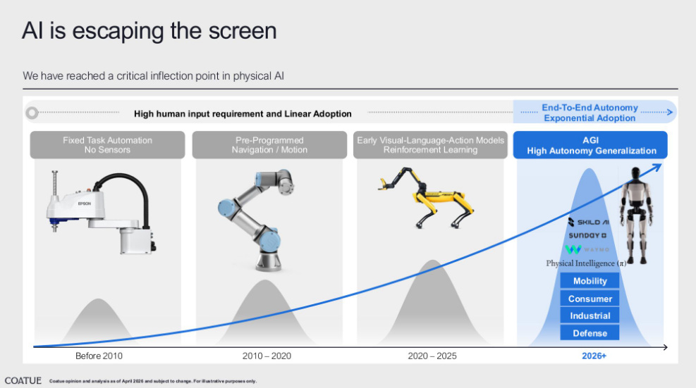
Sony and TSMC Are Building the “Eyes” of Physical AI
索尼與台積電正在打造實體人工智慧的「眼睛」
This is why the long-term implications of the Sony-TSMC partnership may extend well beyond smartphone cameras.
這正是為何索尼與台積電合作的長期影響,可能遠超越智慧型手機相機領域。
Sony itself is already moving deeper into AI vision. In July 2026, Sony Semiconductor Solutions and Mitsubishi Electric announced plans for a separate joint venture developing AI vision-sensor solutions for manufacturing applications—another sign that Sony increasingly sees sensing as part of machine intelligence rather than simply digital photography.
索尼本身已更深入投入 AI 視覺技術。2026 年 7 月,索尼半導體解決方案公司與三菱電機宣布計畫成立另一家合資企業,開發用於製造應用的 AI 視覺感測器解決方案——這再次顯示,索尼日益將感測技術視為機器智慧的一部分,而不僅限於數位攝影。
That direction is logical.
此一發展方向合乎邏輯。
Large language models taught machines to understand human language.
大型語言模型已教會機器理解人類語言。
The next industrial transformation will require machines to understand the physical world.
下一波產業轉型將要求機器能夠理解實體世界。
Robots need cameras.機器人需要相機。
Autonomous vehicles need cameras.
自動駕駛車輛需要攝影機。
Factories need cameras.工廠需要攝影機。
Drones need cameras.無人機需要攝影機。
AR glasses need cameras.AR 眼鏡需要攝影機。
AI agents operating in physical environments need continuous streams of visual information.
在實體環境中運作的 AI 代理需要連續的視覺資訊流。
Before AI can reason about the physical world, something has to capture it.
在 AI 能夠對實體世界進行推理之前,必須先有某種裝置來捕捉它。
That makes the image sensor one of the most strategically important entry points into physical AI.
這使得影像感測器成為進入實體 AI 最具戰略意義的切入點之一。
The Bigger Picture更宏觀的視野
The financial contribution from the Sony-TSMC joint venture will not materially change the semiconductor industry’s 2026 earnings cycle.
索尼與台積電合資企業的財務貢獻,不會對半導體產業 2026 年的獲利週期產生重大影響。
Its strategic significance is much larger.
其戰略意義則遠為重大。
The deal reveals how the next phase of semiconductor competition is evolving.
此交易揭示了半導體競爭下一階段的演進方向。
The first wave of the AI semiconductor boom was about securing GPUs.
AI 半導體浪潮的第一波焦點在於取得 GPU。
The second was about securing HBM and advanced packaging.
第二項是確保高頻寬記憶體(HBM)與先進封裝的供應。
The next phase is increasingly about controlling the complete architecture connecting the physical world to AI computing.
下一階段的重點日益轉向掌控連結實體世界與人工智慧運算的完整架構。
Sensors capture reality.感測器捕捉現實。
Connectivity transports the data.
連線負責傳輸資料。
Memory stores it.記憶體負責儲存資料。
Processors interpret it.處理器負責解讀資料。
Advanced packaging integrates the system.
先進封裝則整合整個系統。
AI software makes the decision.
AI 軟體做出決策。
Seen from this perspective, the Sony-TSMC partnership is not simply another Japanese semiconductor investment.
從這個角度來看,Sony 與台積電的合作夥伴關係不僅僅是另一項日本半導體投資。
It is part of a much broader reorganization of the global technology supply chain.
這是全球科技供應鏈更廣泛重組的一部分。
Japan is attempting to anchor strategic sensor production domestically.
日本正致力於將戰略性感測器生產扎根於本土。
Taiwan is exporting advanced manufacturing capability into allied industrial clusters.
台灣則將先進製造能力輸出至盟國產業聚落。
China is building an increasingly competitive domestic CIS ecosystem and is beginning to win credibility in higher-end applications.
中國正建構日益具競爭力的本土 CIS 生態系,並開始在高階應用領域贏得信譽。
And U.S. technology platforms continue to shape the computing architectures into which those sensors ultimately connect.
而美國技術平台持續塑造這些感測器最終連結的運算架構。
The world is therefore not moving toward a single vertically integrated semiconductor supply chain.
因此,全球並非朝向單一垂直整合的半導體供應鏈發展。
It is moving toward multiple competing technology ecosystems connected by selective interdependence.
而是邁向多個相互競爭的技術生態系,並透過選擇性的相互依存關係彼此連結。
That distinction matters.
這一區別至關重要。
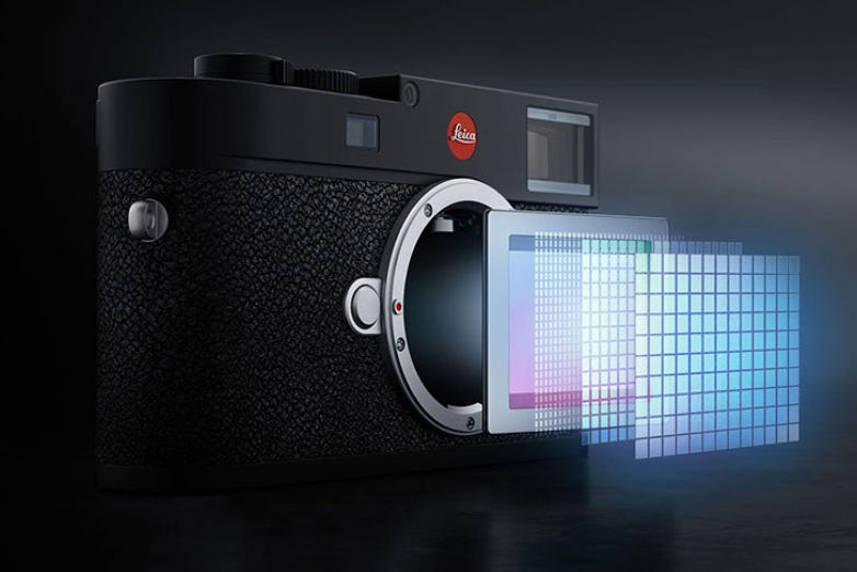
The Leica-Gpixel partnership demonstrates that premium Western companies can still choose Chinese semiconductor technology when performance and customization make commercial sense. The Sony-TSMC partnership simultaneously demonstrates that governments and major semiconductor companies are willing to invest billions to geographically secure strategically important production.
徠卡與長光辰芯的合作表明,當性能與客製化具備商業合理性時,頂級西方企業仍會選擇中國的半導體技術。與此同時,索尼與台積電的合作則顯示,各國政府與主要半導體公司願意投入數十億美元,以確保策略性重要產能的地理安全。
Both trends can exist at the same time.
這兩種趨勢可以同時並存。
And that may be the defining characteristic of the semiconductor industry over the next decade.
這或許將成為未來十年半導體產業的決定性特徵。
The battle is no longer only about who builds the fastest AI processor.
這場競爭已不再僅是誰能打造出最快的 AI 處理器。
It is increasingly about who controls the technologies that allow machines to see, understand and interact with the real world.
愈來愈關鍵的是,誰能掌握讓機器得以看見、理解並與現實世界互動的技術。
TSMC and Sony are now placing a very large bet on who will manufacture those eyes.
台積電與索尼如今正大舉押注,看誰將製造出這些「眼睛」。
SEMIVISION @_@ 是一份由讀者支持的出版物。若要接收最新文章並支持我的工作,歡迎考慮成為免費或付費訂閱者。


Share分享
Previous上一頁Next下一則