Beyond Chips: Washington Expands Semiconductor Security to Polysilicon
Beyond Chips: Washington Expands Semiconductor Security to Polysilicon
- Source: SemiVision
- Author: SEMIVISION
- Published: 2026-08-10T13:28:29+08:00
- URL: https://tspasemiconductor.substack.com/p/beyond-chips-washington-expands-semiconductor
中文翻譯與英文原文(雙語)
(1) 超越晶片:華府將半導體安全範疇擴展至多晶矽 --- (1) Beyond Chips: Washington Expands Semiconductor Security to Polysilicon


Beyond Chips: Washington Expands Semiconductor Security to Polysilicon
超越晶片:華府將半導體安全擴展至多晶矽
Original Article By SemiVision Research [Reading time: 10 mins]
原文作者:SemiVision Research [閱讀時間:10 分鐘]

Aug 10, 2026
Share分享
Beyond Chips: Washington Expands Semiconductor Security to Polysilicon
超越晶片:華府將半導體安全擴展至多晶矽
If the defining semiconductor story of 2025 and 2026 has been AI pushing advanced logic, HBM, and advanced packaging into chronic supply tightness, Washington’s latest move suggests that the next phase of competition may begin much further upstream.
若 2025 與 2026 年半導體產業的主軸,是人工智慧(AI)推動先進邏輯晶片、高頻寬記憶體(HBM)及先進封裝陷入長期供不應求的局面,那麼華盛頓最新的舉措則顯示,下一階段的競爭可能將從更上游的環節展開。
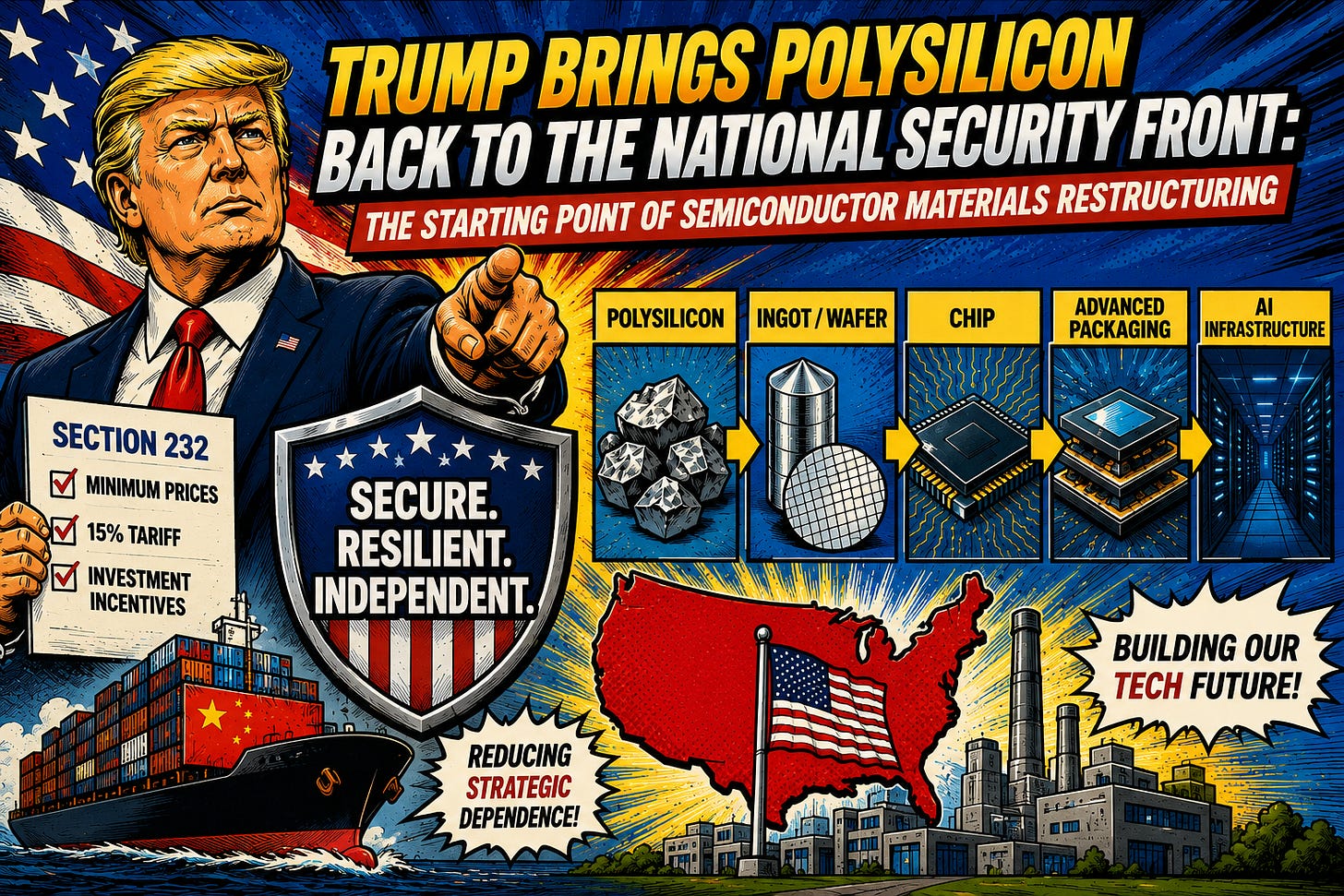
On August 6, 2026, the White House issued a new Section 232 proclamation covering polysilicon and its derivative products, explicitly framing polysilicon as a national-security input for both the semiconductor and solar industries. The measure introduces minimum import prices, additional tariffs on specified downstream derivatives, and an incentive mechanism designed to encourage companies to build or expand production capacity in the United States. Most provisions take effect on December 4, 2026, giving the supply chain roughly 120 days to adjust contracts, inventories, sourcing strategies, and investment plans.
2026 年 8 月 6 日,白宮發布了一項涵蓋多晶矽及其衍生產品的新 232 條款公告,明確將多晶矽定位為半導體與太陽能產業的國家安全投入要素。該措施引入了最低進口價格、針對特定下游衍生產品的額外關稅,以及旨在鼓勵企業在美國興建或擴建產能的激勵機制。大多數條款將於 2026 年 12 月 4 日生效,留給供應鏈約 120 天的時間來調整合約、庫存、採購策略及投資計畫。
ADJUSTING IMPORTS OF POLYSILICON AND ITS DERIVATIVES INTO THE UNITED STATES
At first glance, this looks primarily like another solar-industry trade measure.
乍看之下,這似乎僅是另一項針對太陽能產業的貿易措施。
For the semiconductor industry, however, the more important development is the policy logic behind it.
然而,對半導體產業而言,更重要的發展在於其背後的政策邏輯。
Washington is no longer treating semiconductor security as simply a question of whether enough advanced chips can be fabricated in the United States. The policy perimeter is moving upstream—from GPUs, fabs, lithography tools and packaging capacity toward the fundamental materials required to sustain those manufacturing ecosystems.
華府不再將半導體安全單純視為美國能否生產足夠先進晶片的問題。政策邊界正向上游移動,從 GPU、晶圓廠、微影設備與封裝產能,轉向支撐這些製造生態系所需的基礎材料。
That could mark the beginning of a much broader restructuring of the semiconductor materials supply chain.
這可能標誌著半導體材料供應鏈更廣泛重組的開端。
SEMIVISION @_@ 是一份由讀者支持的出版物。若要接收最新文章並支持我的工作,歡迎考慮成為免費或付費訂閱者。
This Is More Than a Tariff
這不僅是關稅
The August 6 proclamation combines three separate policy mechanisms.
8 月 6 日公告結合了三項獨立的政策機制。
First, the United States establishes minimum import prices, or MIPs, of $21/kg for polysilicon, $100/kg for polysilicon ingots and wafers, $0.22/W for solar cells, and $0.38/W for solar modules. If qualifying imports are entered below those thresholds, importers can effectively face a tariff equal to the difference between the declared value and the applicable minimum price.
首先,美國針對多晶矽設定每公斤 21 美元的最低進口價格(MIP),針對多晶矽錠與晶圓設定每公斤 100 美元,針對太陽能電池設定每瓦 0.22 美元,並針對太陽能模組設定每瓦 0.38 美元。若符合資格的進口產品申報價格低於這些門檻,進口商將面臨相當於申報價值與適用最低價格之間差額的關稅。
Second, beginning December 4, specified polysilicon ingots and downstream derivative products will face an additional 15% Section 232 tariff, subject to country-specific arrangements. Importantly, this should not be interpreted as a blanket additional 15% tariff on every shipment of raw polysilicon.
其次,自 12 月 4 日起,指定的多晶矽錠及下游衍生產品將額外課徵 15% 的 232 條款關稅,惟須視各國具體安排而定。重要的是,此舉不應被解讀為對每一批(raw) 多晶矽貨物全面加徵 15% 的額外關稅。
Third—and perhaps most strategically important—the Department of Commerce is authorized to create an onshoring incentive program. Companies can submit plans to build, expand, or refurbish U.S. facilities producing polysilicon, ingots, wafers, or cells. Approved companies may receive tariff benefits on necessary imports while their U.S. capacity is being constructed. The proclamation requires qualifying projects to begin construction by January 20, 2029.
第三,或許也是最具戰略意義的一點,是授權美國商務部建立一項回流激勵計畫。企業可提交在美國興建、擴建或翻新多晶矽、晶錠、晶圓或電池生產設施的計畫。經核准的企業在其美國產能建設期間,可就必要進口項目獲得關稅優惠。該行政命令要求符合資格的專案必須於 2029 年 1 月 20 日前動工。
This combination matters.
此項組合至關重要。
A conventional tariff simply raises the cost of imports. An MIP plus tariff-offset mechanism tied to domestic investment attempts to change the economics of capital allocation itself.
傳統關稅僅是提高進口成本;而結合最低進口價格(MIP)並與國內投資掛鉤的關稅抵免機制,則旨在改變資本配置本身的經濟邏輯。
Washington is effectively telling companies: importing will become more expensive, but companies willing to establish manufacturing capacity inside the United States may receive preferential treatment.
華府實際上是在向企業傳達:進口將變得更為昂貴,但願意在美國境內建立製造產能的企業,則可能獲得優先待遇。
That is industrial policy, not simply trade protection.
這是產業政策,而不僅僅是貿易保護。
Why Polysilicon Has Entered the Semiconductor Security Debate
為何多晶矽已進入半導體安全辯論
The policy document explicitly describes polysilicon as the base material underpinning both America’s semiconductor and solar-power supply chains.
該政策文件明確將多晶矽描述為支撐美國半導體與太陽能供應鏈的基礎材料。

That wording is significant.
該措辭至關重要。
The White House notes that the U.S. share of global polysilicon production capacity fell from roughly 50% in 2005 to less than 2% in 2024. It also states that America’s share of global semiconductor wafer-fabrication capacity declined from 37% in 1990 to roughly 10% in 2024.
白宮指出,美國在全球多晶矽產能中的佔比已從 2005 年的約 50% 下滑至 2024 年的不到 2%。同時聲明,美國在全球半導體晶圓製造產能的佔比也從 1990 年的 37% 降至 2024 年的約 10%。
But another number buried inside the proclamation may be even more important for semiconductor investors.
然而,公告中隱藏的另一項數據對半導體投資人而言可能更為關鍵。
According to the Commerce Department findings cited by the White House, semiconductor-grade polysilicon now represents only about2.4% of global polysilicon production. Solar-grade material dominates industry volumes. As a result, the economics of high-purity semiconductor polysilicon cannot necessarily be separated from the much larger solar polysilicon ecosystem.
根據白宮引用的商務部調查結果,半導體級多晶矽目前僅佔全球多晶矽產量的約 2.4%,太陽能級材料則主導了整體產業規模。因此,高純度半導體多晶矽的經濟性未必能與規模龐大得多的太陽能多晶矽生態系統割裂開來。
This creates an unusual industrial-policy linkage.
這造就了一種罕見的產業政策連結。
A country may want secure access to semiconductor-grade polysilicon, but maintaining economically viable domestic producers can also depend on having sufficient scale in lower-purity solar-grade production.
一個國家可能希望確保取得半導體級多晶矽,但要維持具經濟可行性的國內生產商,也可能取決於是否具備足夠規模的低純度太陽能級多晶矽產能。
In other words, energy security and semiconductor security increasingly share the same upstream industrial base.
換言之,能源安全與半導體安全日益仰賴相同的上游產業基礎。
That helps explain why Washington is addressing solar cells, ingots, wafers, and semiconductor materials through the same policy framework.
這有助於解釋為何華盛頓透過同一政策框架,同時處理太陽能電池、晶錠、晶圓及半導體材料。
The Semiconductor Security Perimeter Keeps Expanding
半導體安全邊界持續擴張
This did not begin in August.
這並非始於八月。
On January 14, 2026, the White House had already acted under Section 232 following an investigation into imports of semiconductors, semiconductor manufacturing equipment, and derivative products. The administration explicitly argued that insufficient domestic semiconductor and equipment capacity created excessive dependence on foreign supply chains and represented a national-security vulnerability.
2026 年 1 月 14 日,白宮已依據針對半導體、半導體製造設備及其衍生產品進口所進行的調查,採取第 232 條行動。政府明確主張,國內半導體與設備產能不足,導致過度依賴外國供應鏈,構成國家安全漏洞。
The polysilicon action extends that logic another step upstream.
多晶矽行動將此邏輯進一步向上游推進。
The strategic question is therefore changing.
因此,戰略問題正在發生轉變。
For several years, semiconductor supply-chain discussions have focused on whether the United States can manufacture enough advanced logic chips, whether CoWoS and other advanced packaging capacity can expand quickly enough, whether HBM supply can catch up with AI accelerator demand, and whether leading-edge lithography and manufacturing equipment remain accessible.
數年來,半導體供應鏈的討論焦點一直集中在:美國能否生產足夠的先進邏輯晶片、CoWoS 及其他先進封裝產能能否快速擴張、HBM 供應能否追上 AI 加速器的需求,以及領先製程的微影與製造設備是否仍能取得。
Those constraints remain critical.
這些限制仍然至關重要。
But Washington is increasingly asking a more fundamental question:
但華盛頓正日益提出一個更根本的問題:
What happens if the materials beneath those manufacturing processes are themselves concentrated in supply chains that policymakers consider strategically vulnerable?
倘若這些製程底下的材料,其供應鏈本身集中於政策制定者認為具戰略脆弱性的來源,將會發生什麼情況?
Once governments start asking that question, the potential national-security perimeter becomes much larger.
一旦各國政府開始提出這個問題,潛在的國家安全邊界將大幅擴大。
It can include silicon wafers, high-purity chemicals, specialty gases, photoresists, advanced substrates, copper foil, glass fabrics, packaging materials, rare metals, power electronics materials, and potentially many other upstream inputs.
其範圍可涵蓋矽晶圓、高純度化學品、特種氣體、光阻劑、先進基板、銅箔、玻璃纖維布、封裝材料、稀有金屬、功率電子材料,以及潛在的眾多其他上游投入要素。
Polysilicon may therefore be less important as an isolated event than as a precedent.
因此,多晶矽的重要性與其說是單一事件,不如說是作為先例。
7月28日7 月 28 日
AI Is Moving From a Chip Race to a System Race
AI 競爭正從晶片競賽轉向系統競賽
The timing is particularly interesting because semiconductor technology itself is moving toward greater system-level integration.
此時機格外引人注目,因為半導體技術本身正朝向更高層級的系統整合邁進。
At FMS 2026, Samsung introduced concept models for zHBM and zNAND-O and unveiled its 400-plus-layer V10 BV-NAND architecture. Samsung’s zHBM concept moves memory beyond the conventional side-by-side accelerator-and-HBM configuration toward vertical integration above the AI accelerator, illustrating how future AI architectures increasingly depend on the co-optimization of logic, memory, packaging, interconnects and thermal management.
在 2026 年快閃記憶體高峰會(FMS 2026)上,三星發表了 zHBM 與 zNAND-O 的概念模型,並揭曉其擁有超過 400 層的 V10 BV-NAND 架構。三星的 zHBM 概念將記憶體從傳統加速器與 HBM 並列的配置,轉向垂直整合至 AI 加速器上方,彰顯未來 AI 架構日益依賴邏輯、記憶體、封裝、互連及散熱管理的共同優化。
During the same FMS week, Sandisk and SK hynix released the first technical specification for High Bandwidth Flash through the Open Compute Project. HBF is being positioned as a memory tier between HBM and SSD storage, attempting to bring much larger NAND-based capacity closer to AI processors while maintaining significantly higher bandwidth than conventional storage architectures.
在同一週的 FMS 期間,SanDisk 與 SK hynix 透過開放運算專案(Open Compute Project)發布了高頻寬快閃記憶體(High Bandwidth Flash, HBF)的首份技術規格。HBF 被定位為介於 HBM 與 SSD 儲存之間的記憶體層級,旨在將基於 NAND 的大容量儲存更靠近 AI 處理器,同時維持遠高於傳統儲存架構的頻寬。
8月9日8 月 9 日
These developments point in the same direction.
這些發展都指向同一個方向。
AI infrastructure competition is no longer about purchasing the fastest GPU in isolation.
AI 基礎設施的競爭已不再只是單純採購最快的 GPU。
It is becoming a competition over memory hierarchy, data movement, packaging, thermal architecture, power delivery and manufacturing scale.
這已演變為一場關於記憶體階層、資料傳輸、封裝技術、散熱架構、電源供應以及製造規模的競爭。
The polysilicon decision adds another layer to that system competition: the geographic security of the materials used to build the system.
多晶矽決策為這場體系競爭增添了另一層面:用於建構該體系之材料的地理安全性。

7月9日7 月 9 日
The Impact on Asia Will Not Be Uniform
對亞洲的影響將非均質
China retains enormous scale advantages across many upstream manufacturing and materials categories. Stronger U.S. localization policies could encourage Chinese companies to deepen domestic integration while redirecting incremental capacity toward China’s internal market and other regions less exposed to U.S. trade restrictions.
中國在眾多上游製造與材料類別中仍保有顯著的規模優勢。美國更強力的在地化政策,可能促使中國企業深化國內整合,同時將新增產能轉向中國內需市場及其他較不易受美國貿易限制影響的地區。
The likely result is not simply reshoring.
可能的結果並非單純的回流(reshoring)。
It may be the development of increasingly parallel industrial ecosystems.
而是可能發展出日益平行的產業生態系。
One supply chain would optimize around the United States and its preferred partners. Another would optimize around China and markets willing to remain integrated with Chinese manufacturing.
其中一條供應鏈將圍繞美國及其優先合作夥伴進行優化;另一條則將圍繞中國,以及願意持續與中國製造業保持整合的市場進行優化。
Japan and Korea occupy a different position.
日本與韓國處於不同的地位。
Both have substantial capabilities in high-purity semiconductor materials, wafers, chemicals, equipment and specialty components. As the United States attempts to reduce exposure to strategically sensitive Chinese supply chains, Japanese and Korean suppliers could become increasingly valuable as technically qualified, non-Chinese sources.
兩國在高純度半導體材料、晶圓、化學品、設備及特殊元件方面皆具備雄厚實力。隨著美國試圖降低對戰略敏感之中國供應鏈的依賴,日韓供應商作為技術合格且非中國的來源,其價值將日益提升。
The August proclamation itself reinforces this distinction.
八月公告本身即強化了此項區別。
For products from Japan, Korea, Taiwan, Switzerland, Liechtenstein and EU member states, the combined applicable ordinary tariff and additional Section 232 tariff is generally structured to equal 15%, rather than simply stacking an additional 15% on top of existing duties. The United Kingdom receives a separate 10% Section 232 rate.
針對來自日本、韓國、台灣、瑞士、列支敦斯登及歐盟成員國的產品,其適用的普通關稅與額外 232 條款關稅合計通常設定為 15%,而非在既有關稅基礎上簡單加徵 15%。英國則適用獨立的 10% 232 條款稅率。
This suggests the policy is not simply about shutting foreign suppliers out.
這顯示該政策並非單純旨在將外國供應商排除在外。
It is also about redesigning the hierarchy of acceptable foreign supply.
這也涉及重新設計可接受的外國供應層級。
That is essentially friend-shoring embedded into tariff architecture.
這本質上是將友岸外包嵌入關稅架構之中。
Where Taiwan Fits台灣的定位
Taiwan’s strategic importance is unlikely to come from becoming a major commodity polysilicon producer.
台灣的戰略重要性不太可能來自成為多晶矽大宗商品的生產大國。
Its relevance lies further downstream.
其關聯性更進一步延伸至下游。
If Washington increasingly treats materials security, wafer security, semiconductor manufacturing and advanced packaging as parts of one integrated national-security framework, Taiwan’s ecosystem of silicon wafers, specialty chemicals, equipment components, substrates, advanced packaging and semiconductor testing becomes even more strategically significant.
若華府日益將材料安全、晶圓安全、半導體製造與先進封裝視為單一整合的國家安全架構之一環,台灣在矽晶圓、特殊化學品、設備零組件、基板、先進封裝及半導體測試領域的生態系,其戰略重要性將更為凸顯。
The important question for Taiwanese companies will therefore not simply be:
因此,對台灣企業而言,關鍵問題將不再只是:
Can we sell into the U.S. market?
我們能否進入美國市場?
It will increasingly become:
而將逐漸轉變為:
Can we demonstrate that our materials, production locations, upstream sources and ownership structure meet the sourcing requirements of a U.S.-aligned semiconductor supply chain?
我們能否證明我們的材料、生產地點、上游來源及所有權結構,符合與美國結盟之半導體供應鏈的採購要求?
That distinction could influence where companies build new plants, which suppliers they qualify, how customers structure long-term agreements, and even how products are priced.
此項區別可能影響企業新廠的選址、合格供應商的認定、客戶長期合約的架構,甚至產品定價策略。
Supply-chain provenance may gradually become almost as important as technical specification.
供應鏈溯源的重要性將逐漸與技術規格並駕齊驅。
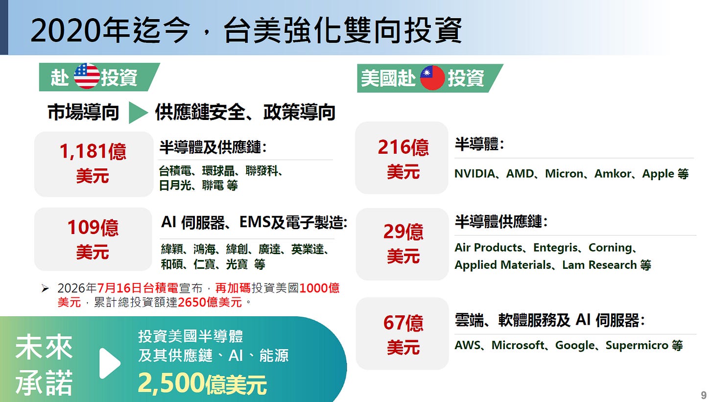
Since 2020, Taiwan and the United States have significantly expanded two-way investment, driven by semiconductor supply-chain security and AI growth. Taiwanese companies have invested heavily in U.S. semiconductor, server, and electronics manufacturing, while U.S. firms continue investing in Taiwan’s semiconductor ecosystem, cloud services, and AI infrastructure. Future Taiwanese commitments in the U.S. could exceed US$250 billion.
自 2020 年以來,在半導體供應鏈安全與人工智慧成長的驅動下,台灣與美國大幅擴大雙向投資。台灣企業大舉投資美國的半導體、伺服器及電子製造業,而美商則持續投入台灣的半導體生態系、雲端服務與人工智慧基礎設施。未來台灣對美國的承諾投資金額可能超過 2,500 億美元。
A Supply-Side Policy Arrives During a Demand Boom
需求繁榮之際,供給面政策應運而生
The timing also increases the potential market impact.
此時間點也增加了潛在的市場衝擊。
On August 6, the Semiconductor Industry Association reported that worldwide semiconductor sales reached $403.3 billion in Q2 2026, up 35.1% from Q1. June sales reached $134.5 billion, an extraordinary 123.6% increase from June 2025 and 9.7% higher than May. SIA said global semiconductor revenue is expected to exceed $1.5 trillion in 2026.
8 月 6 日,半導體產業協會(SIA)報告指出,2026 年第二季全球半導體銷售額達 4,033 億美元,較第一季成長 35.1%。6 月份銷售額達 1,345 億美元,較 2025 年 6 月大幅成長 123.6%,並較 5 月高出 9.7%。SIA 表示,預計 2026 年全球半導體營收將超過 1.5 兆美元。
This means the industry is not absorbing new trade restrictions during a weak demand cycle.
這意味著產業並非在需求疲弱的週期中承受新的貿易限制。
It is doing so while AI investment, semiconductor capital expenditure and infrastructure spending remain extremely strong.
在人工智慧投資、半導體資本支出與基礎設施開支仍維持極強勁之際,美國正採取此項行動。
That matters because upstream disruptions become more economically significant when downstream capacity is already tight.
此事至關重要,因為當下游產能已然緊俏時,上游供應鏈的中斷將產生更顯著的經濟影響。
Changes in material prices, lead times or approved sourcing locations can propagate through the chain into inventory accumulation, renegotiated long-term agreements, customer qualification programs and ultimately product pricing.
材料價格、交貨週期或核准來源地的變動,會沿著供應鏈傳導,進而引發庫存累積、長期合約重新協商、客戶認證計畫調整,並最終影響產品定價。
For investors, the issue is therefore not whether polysilicon will suddenly become a major percentage of an advanced GPU’s bill of materials.
對投資人而言,問題關鍵不在於多晶矽是否會突然佔先進 GPU 物料清單的重大比重。
It will not.不會。
The issue is whether the rules governing semiconductor material sourcing are becoming structurally more restrictive.
關鍵問題在於,規範半導體材料採購的法規是否在結構上趨於更加嚴格。
The August 6 action suggests that they are.
8 月 6 日的行動顯示確實如此。
What We Are Watching Next
接下來我們將關注的重點
Over the next twelve months, four indicators deserve particular attention.
在未來十二個月內,有四項指標特別值得關注。
First, watch which companies submit U.S. onshoring plans and whether major polysilicon, ingot or wafer suppliers announce new American capacity. The difference between policy ambition and actual industrial reconstruction will ultimately be measured in announced facilities, construction starts, customer qualifications and production volumes.
首先,觀察哪些企業提交美國在地化生產計畫,以及主要的多晶矽、晶錠或晶圓供應商是否宣布新增美國產能。政策抱負與實際產業重建之間的落差,最終將透過已宣布的設施、動工情況、客戶認證資格及產量來衡量。
Second, watch whether Washington connects materials policy more directly with semiconductor tariffs, CHIPS-related incentives, procurement preferences and export controls. If these instruments begin operating together, the United States will be moving from individual policy actions toward an integrated semiconductor industrial-security architecture.
其次,觀察華盛頓是否將材料政策更直接地與半導體關稅、《晶片法案》(CHIPS)相關激勵措施、採購偏好及出口管制相連結。若這些工具開始協同運作,美國將從單一的 policy 行動轉向建構整合型的半導體產業安全架構。
Third, watch for further bifurcation across Asian supply chains. Companies serving U.S. customers may increasingly qualify non-Chinese material sources, while supply chains serving China deepen domestic sourcing.
第三,留意亞洲供應鏈進一步分化的跡象。服務美國客戶的企業可能日益傾向認證非中國的材料來源,而服務中國的供應鏈則將深化在地採購。
Fourth, watch procurement contracts.
第四,關注採購合約。
If hyperscalers, semiconductor companies, OSATs and substrate manufacturers begin incorporating country of origin, material provenance or approved-source requirements into multi-year supply agreements, geopolitical alignment will have moved from government policy directly into commercial semiconductor procurement.
若超大型雲端服務業者、半導體公司、OSAT 廠商及基板製造商開始將原產地、材料來源或核准供應商等要求納入多年期供應合約,地緣政治結盟將從政府政策直接延伸至商業半導體採購領域。
That would be one of the clearest signs that the industry has entered a new phase.
這將是產業邁入新階段最明確的信號之一。
7月22日7 月 22 日
SemiVision ViewSemiVision 視角
Our view is that semiconductor competition in the second half of 2026 will increasingly be defined by something broader than the ability to design the most powerful AI chip.
我們認為,2026 年下半年的半導體競爭將日益取決於更廣泛的因素,而不僅是設計出最強大 AI 晶片的能力。
The winners will be the companies—and eventually the national ecosystems—that can manufacture those chips repeatedly, at scale, using supply chains that are technologically capable, economically sustainable and politically acceptable.
勝出者將是那些能夠利用具備技術能力、經濟可持續性且政治可接受的供應鏈,大規模且穩定地製造這些晶片的企業——並最終是具備此能力的國家生態系。
That means the strategic semiconductor stack is expanding.
這意味著戰略性的半導體堆疊正在擴展。
GPU → HBM → advanced packaging → wafers → equipment → chemicals → raw materials → power infrastructure.
GPU → HBM → 先進封裝 → 晶圓 → 設備 → 化學品 → 原材料 → 電力基礎設施。
Each layer is becoming part of the same AI industrial-security equation.
每一層正逐漸成為同一個 AI 產業安全方程式的一部分。
Polysilicon itself may never become the headline bottleneck of the AI semiconductor cycle.
多晶矽本身可能永遠不會成為 AI 半導體週期的頭條瓶頸。
But Washington’s decision to bring it formally inside the Section 232 national-security framework may be one of the earliest signals that the next semiconductor supply-chain restructuring has already begun.
但華盛頓決定將其正式納入《232 條款》國家安全框架,可能是下一個半導體供應鏈重組已經開始的最早訊號之一。
7月4日7 月 4 日
Thanks for reading SEMIVISION @_@! This post is public so feel free to share it.
感謝閱讀 SEMIVISION @_@!本文為公開文章,歡迎自由分享。


Share分享
Previous上一頁