FMS 2026 Signals the Next AI Memory War: Tiered Memory, zHBM, and Advanced Packaging
FMS 2026 Signals the Next AI Memory War: Tiered Memory, zHBM, and Advanced Packaging
- Source: SemiVision
- Author: SEMIVISION
- Published: 2026-08-09T15:53:48+08:00
- URL: https://tspasemiconductor.substack.com/p/fms-2026-signals-the-next-ai-memory
中文翻譯與英文原文(雙語)
(1) FMS 2026 預示下一場 AI 記憶體大戰:分層記憶體、zHBM 與先進封裝 --- (1) FMS 2026 Signals the Next AI Memory War: Tiered Memory, zHBM, and Advanced Packaging


FMS 2026 Signals the Next AI Memory War: Tiered Memory, zHBM, and Advanced Packaging
FMS 2026 預示下一場 AI 記憶體大戰:分層記憶體、zHBM 與先進封裝
Original Article By SemiVision Research [Reading time: 16 mins]
原文作者:SemiVision Research [閱讀時間:16 分鐘]

Aug 09, 2026
∙ Paid∙ 付費
Share分享
FMS 2026 Signals the Next AI Memory War: Tiered Memory, zHBM, and Advanced Packaging
FMS 2026 揭開下一場 AI 記憶體大戰:分層記憶體、zHBM 與先進封裝
If the defining question for AI semiconductors in 2024 and 2025 was “Who can secure more HBM?”, the question emerging in the second half of 2026 is becoming much broader:
如果 2024 年和 2025 年 AI 半導體的關鍵問題是「誰能取得更多 HBM?」,那麼 2026 年下半年浮現的問題則變得更加廣泛:
Even if HBM capacity continues to expand, how much longer can AI systems scale around a single dominant memory architecture?
即使 HBM 容量持續擴張,AI 系統還能圍繞單一主導記憶體架構擴展多久?

6月30日6 月 30 日
Over the past two years, the AI server value chain has revolved around GPUs and HBM. Investors focused on HBM3E and HBM4 supply, pricing, yields, customer qualifications, and capacity allocation. Capital expenditure followed the same direction, flowing into advanced DRAM, CoWoS and other 2.5D packaging capacity, ABF substrates, testing equipment, cooling systems, and AI server infrastructure.
過去兩年,AI 伺服器價值鏈圍繞著 GPU 與 HBM 發展。投資人聚焦於 HBM3E 和 HBM4 的供應、定價、良率、客戶認證及產能配置。資本支出亦遵循相同方向,流入先進 DRAM、CoWoS 及其他 2.5D 封裝產能、ABF 基板、測試設備、散熱系統以及 AI 伺服器基礎設施。
But the workload is changing.
但工作負載正在改變。
AI is moving from training toward massive-scale inference, from single-turn prompts toward agentic AI, and from relatively short context windows toward applications that continuously maintain large amounts of state, memory and KV cache.
AI 正從訓練轉向大規模推論,從單輪提示轉向代理型 AI(agentic AI),並從相對較短的上下文視窗,轉向需要持續維持大量狀態、記憶體與 KV 快取的應用。
That changes the bottleneck.
這改變了瓶頸所在。
The challenge is no longer simply whether enough HBM can be placed next to a GPU. Increasingly, the question is whether different classes of memory—with different bandwidth, latency, capacity, cost and power characteristics—can be orchestrated efficiently as one system.
挑戰已不再只是能否在 GPU 旁放置足夠的 HBM。越來越多的問題在於,能否將具有不同頻寬、延遲、容量、成本與功耗特性的各類記憶體,有效協調為單一系統。
That was arguably the most important message coming out of FMS 2026.
這可說是 FMS 2026 所傳達的最重要訊息。
Rather than treating HBM, DRAM, NAND, SSD and CXL memory as separate product categories, the industry is beginning to treat them as components of a much larger AI memory hierarchy.
產業界正開始不再將 HBM、DRAM、NAND、SSD 與 CXL 記憶體視為獨立的產品類別,而是將其視為更龐大 AI 記憶體階層架構中的組成元件。
And that could become the next major semiconductor battleground.
而這可能成為下一個半導體的主要戰場。
FMS 2026:The Conversation Moved Beyond HBM
FMS 2026:對話已超越 HBM
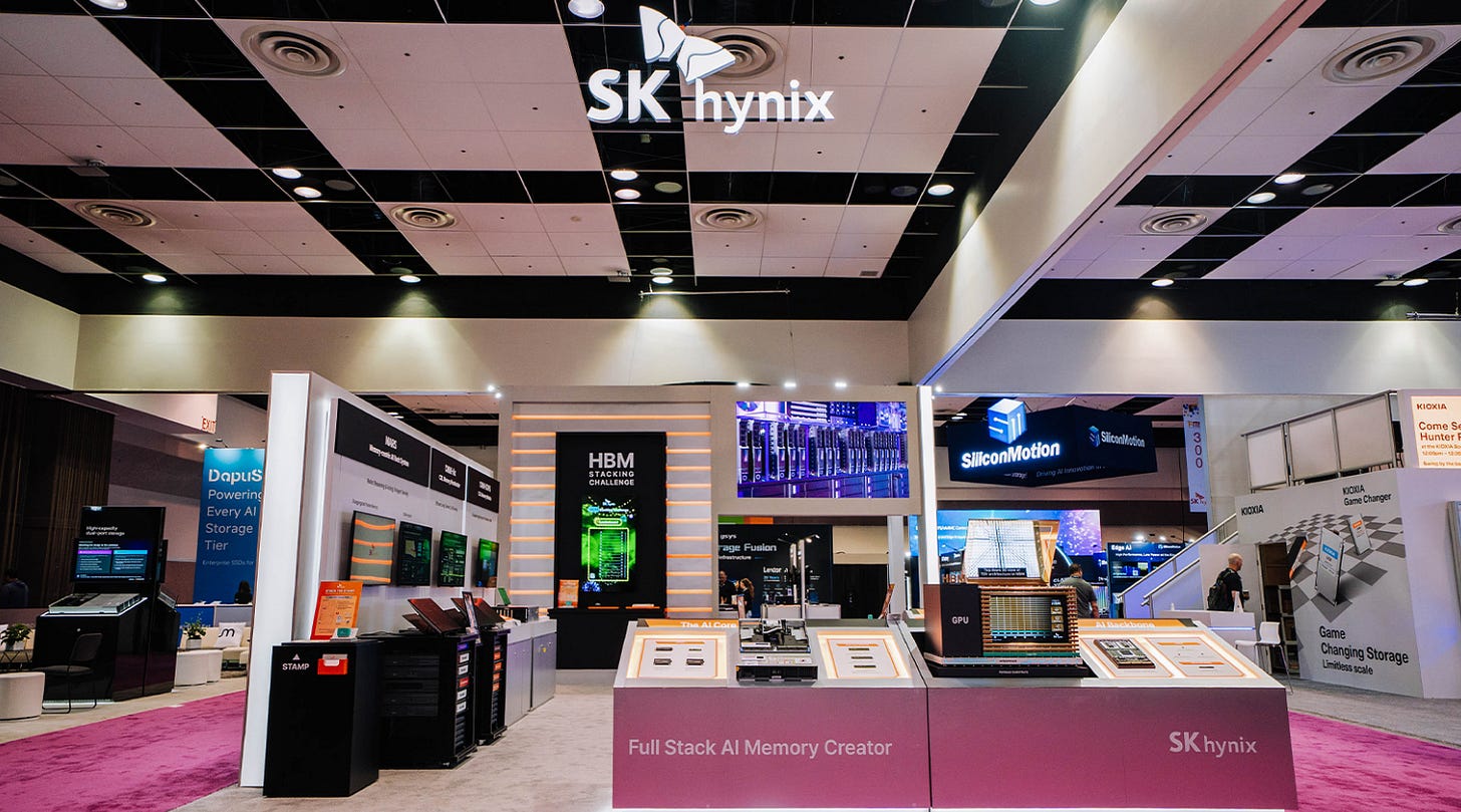
At FMS 2026, held August 4–6 in Santa Clara, SK hynix’s keynote was particularly revealing.
於 8 月 4 日至 6 日在聖塔克拉拉舉行的 FMS 2026 大會上,SK hynix 的主題演講尤具啟發性。

The company framed its strategy around Tiered Memory, arguing that as agentic AI becomes more complex, no single memory technology can economically satisfy every requirement.
該公司將其策略圍繞「分層記憶體」(Tiered Memory)展開,主張隨著代理式 AI(agentic AI)日益複雜,單一記憶體技術已無法在經濟層面上滿足所有需求。
Its proposed hierarchy includes HBM, conventional DRAM, NAND-based technologies such as High Bandwidth Flash, enterprise SSDs and CXL-attached memory. The objective is not simply to maximize the speed of every layer. It is to place data in the appropriate memory tier and minimize unnecessary data movement across the system.
其提出的架構包含 HBM、傳統 DRAM、基於 NAND 的技術(例如高頻寬快閃記憶體 High Bandwidth Flash)、企業級 SSD,以及透過 CXL 連接的記憶體。此目標並非單純最大化每一層的速度,而是將數據置於適當的記憶體層級,並最小化系統中不必要的數據移動。
That distinction matters.
這一區別至關重要。
SK hynix is effectively saying that future AI infrastructure competitiveness will increasingly depend on memory orchestration rather than memory performance alone.
SK hynix 實際上是在表示,未來 AI 基礎設施的競爭力將越來越取決於記憶體協調(memory orchestration),而不僅僅是記憶體效能。
Sandisk delivered a similar message during its FMS keynote, arguing that high-context models and agentic workloads are shifting the constraint from pure compute toward memory capacity, bandwidth and even what it calls “token economics.” NAND, in this model, is no longer simply cold storage sitting far below the accelerator. It can become an active component of the AI memory hierarchy.
Sandisk 在其 FMS 主題演講中傳達了類似訊息,主張高上下文模型與代理型工作負載正將瓶頸從純粹的運算能力轉向記憶體容量、頻寬,甚至是其所稱的「代幣經濟」(token economics)。在此架構下,NAND 不再只是位於加速器下方遠端的冷儲存裝置;它可成為 AI 記憶體階層中的活躍組件。
This is one reason FMS 2026 felt different from the HBM-centric discussion of the previous two years.
這正是 FMS 2026 給人有別於過去兩年以 HBM 為中心討論的原因之一。
HBM remains critical—but the industry is beginning to design around what comes before, beside and after HBM.
HBM 依然至關重要,但產業界正開始針對 HBM 之前、旁邊及之後的環節進行設計。
Below we will share:以下我們將分享:
HBF Could Create an Entirely New Memory Tier
HBF 有望開創全新的記憶體層級
CXL Is Moving From PowerPoint to AI Workloads
CXL 正從簡報概念邁向實際 AI 工作負載
Samsung Goes in the Opposite Direction: Bring Memory Even Closer
三星採取相反策略:將記憶體佈建得更為緊密
CXL Is Moving From PowerPoint to AI Workloads
CXL 正從簡報走向 AI 工作負載
Why This Matters for Taiwan
為何這對台灣至關重要
Five Signals to Watch Next
接下來值得關注的五大訊號
The Next Memory War Is About Architecture
下一場記憶體大戰將是架構之戰
FMS 2026 Storage Summit: Four Key Takeaways
FMS 2026 儲存高峰會:四大重點摘要

7月28日7 月 28 日

7月24日7 月 24 日

7月9日7 月 9 日
HBF Could Create an Entirely New Memory Tier
HBF 可能開創全新的記憶體層級
One of the most interesting announcements was High Bandwidth Flash, or HBF.
其中最引人注目的發表之一是高頻寬快閃記憶體(High Bandwidth Flash,簡稱 HBF)。
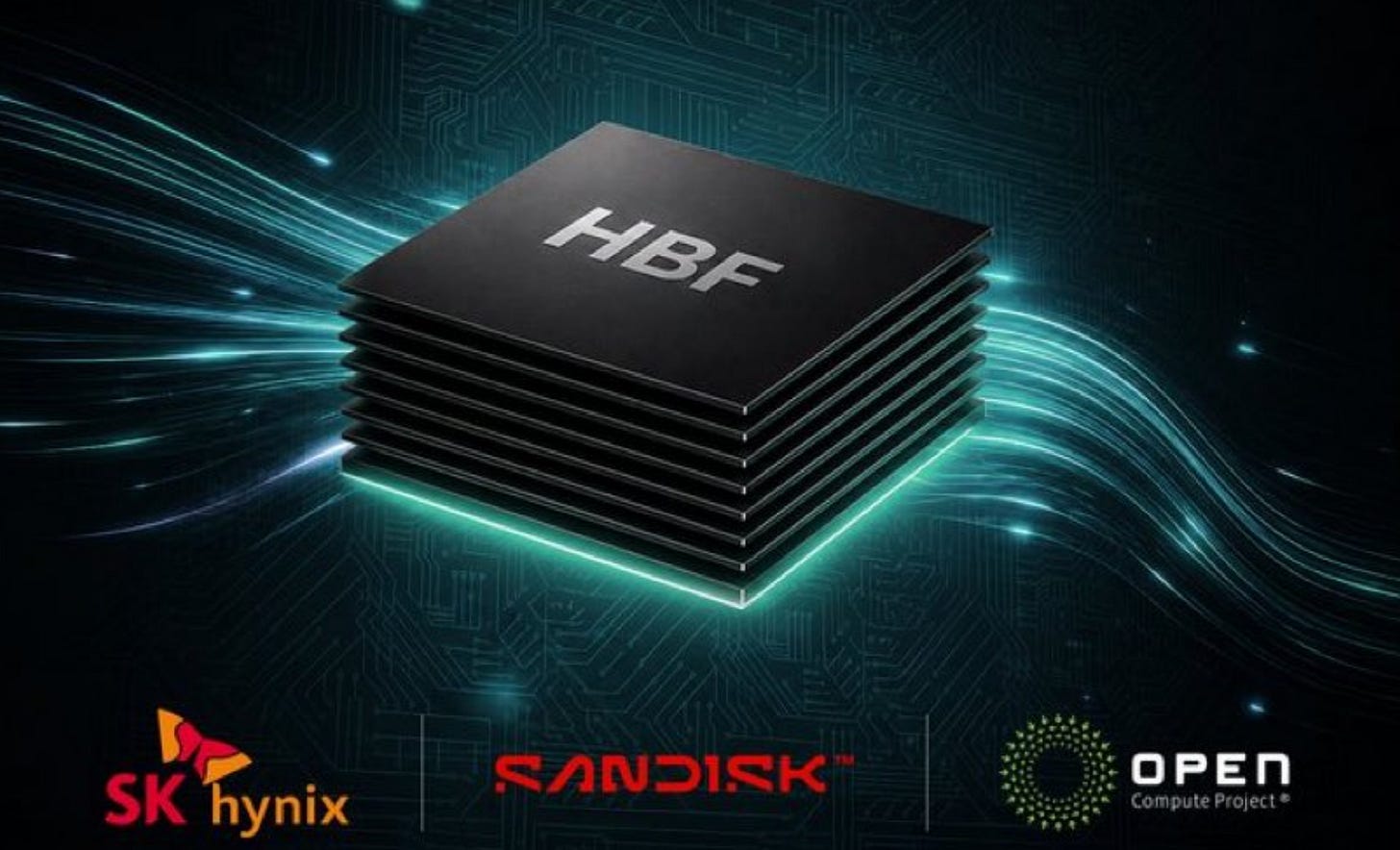
SK hynix and Sandisk released the first open HBF specification through the Open Compute Project at FMS. The current specification supports 8-high and 16-high NAND stacks, capacities of up to 512GB, and three bandwidth grades ranging from roughly 0.4TB/s to 3.0TB/s.
SK hynix 與 Sandisk 於 FMS 透過開放運算專案(Open Compute Project)發布了首版開放式 HBF 規格。現行規格支援 8 層與 16 層 NAND 堆疊,容量最高可達 512GB,並提供三種頻寬等級,範圍約從 0.4TB/s 至 3.0TB/s。
Perhaps more importantly, HBF uses UCIe as its processor interconnect, creating a potential path for integration with CPUs, GPUs and other chiplet-based accelerators. Google and Tenstorrent are already participating in the HBF consortium.
或許更重要的是,HBF 採用 UCIe 作為其處理器互連技術,為與 CPU、GPU 及其他基於小晶片(chiplet)的加速器整合開闢了潛在路徑。Google 和 Tenstorrent 已加入 HBF 聯盟。
That makes HBF more than another NAND product.
這使得 HBF 不僅是另一項 NAND 產品。

HBF is trying to solve a different problem. Not replacing HBM with NAND — but bringing massive, lower-cost NAND capacity much closer to the GPU.
HBF 旨在解決不同的問題:並非以 NAND 取代 HBM,而是將大容量、低成本的 NAND 容量更貼近 GPU。
Sandisk’s own illustration makes the idea very intuitive:
SanDisk 自身的圖示讓這個概念變得非常直觀:
HBM: 192GBHBM:192GB
HBF + HBM concept: 3,120GB
HBF + HBM 概念:3,120GB
HBF concept: 4,096GBHBF 概念:4,096GB
The point isn’t that HBF is faster than HBM.
重點不在於 HBF 比 HBM 更快。
The point is capacity.重點在於容量。
Architecturally, it is attempting to occupy the enormous gap between extremely fast but expensive HBM and extremely high-capacity but comparatively distant SSD storage.
在架構上,它旨在填補速度極快但昂貴的 HBM 與容量極大但相對遙遠的 SSD 儲存之間的巨大落差。
The objective is straightforward: retain much of NAND’s capacity and cost advantage while dramatically increasing bandwidth through stacked dies, TSVs, base-die logic and advanced packaging.
目標非常明確:在保留 NAND 大部分容量與成本優勢的同時,透過堆疊晶粒、TSV、基底晶粒邏輯與先進封裝技術,大幅提升頻寬。
In effect, HBF is trying to break today’s relatively simple model:
實際上,HBF 正試圖打破現今相對簡單的架構模式:
HBM for hot data. SSD for cold data.
HBM 用於熱數據,SSD 用於冷數據。
If HBF succeeds, there could be a new layer in the middle.
若 HBF 成功,將可能在兩者之間新增一個層級。
That could have significant implications for inference.
這可能對推論產生重大影響。
Large language model serving increasingly involves enormous model weights and KV caches. Not all of this data requires HBM-level latency at every moment, but moving it repeatedly between conventional storage and GPU memory consumes bandwidth, power and time.
大型語言模型的服務日益涉及龐大的模型權重與 KV 快取。並非所有這些資料在每個時刻都需要 HBM 等級的延遲,但將其反覆於傳統儲存裝置與 GPU 記憶體之間移動,會消耗頻寬、電力與時間。
A high-capacity intermediate memory tier could therefore improve accelerator utilization without requiring every byte of working data to reside in premium HBM.
因此,一個高容量的中階記憶體層級可以提升加速器的利用率,而無需讓所有工作資料都駐留在昂貴的 HBM 中。
This is why HBF should be watched as an architectural technology rather than merely a NAND technology.
這就是為什麼 HBF 應被視為一種架構技術,而不僅僅是 NAND 技術。

The ecosystem signal is equally important. The FMS panel on HBF included SK hynix, Sandisk and Google DeepMind, while the specification itself is being developed as an open industry standard rather than a proprietary interface.
生態系的訊號同樣重要。關於 HBF 的 FMS 小組討論成員包括 SK hynix、Sandisk 和 Google DeepMind,而其規格正被開發為開放式產業標準,而非專有介面。
The key question is now whether GPU vendors, hyperscalers and custom ASIC designers begin building HBF support into actual platforms.
關鍵問題在於,GPU 供應商、超大型雲端服務業者及客製化 ASIC 設計商是否開始將 HBF 支援整合至實際平台中。
If they do, HBF could create a new memory category.
若成真,HBF 將開創全新的記憶體類別。
CXL Is Moving From PowerPoint to AI Workloads
CXL 正從簡報概念邁向實際 AI 工作負載
The second major FMS signal came from SK hynix’s CXL demonstrations.
FMS 展會的第二個重要訊號來自 SK hynix 展示的 CXL 技術。
The company demonstrated a distributed AI-agent serving architecture using CXL pooled memory, allowing multiple servers and GPUs to share memory capacity and reuse KV cache without relying entirely on conventional network communication.
該公司展示了採用 CXL 池化記憶體的分散式 AI 代理服務架構,使多台伺服器與 GPU 能夠共享記憶體容量並重複使用 KV 快取,而無需完全依賴傳統的網路通訊。
It also demonstrated CMM-Hybrid, combining DRAM and SSD behind a CXL-based architecture. The system predicts which KV-cache data will be required, prefetches that data into DRAM and keeps larger volumes on SSD.
該系統亦展示了 CMM-Hybrid,此架構透過基於 CXL 的技術將 DRAM 與 SSD 結合。系統會預測哪些 KV-cache 資料將被需要,並將這些資料預取至 DRAM,同時將更大容量的資料保留在 SSD 上。
Another demonstration targeted long-context LLM serving using CMM-Ax, which integrates computing capability into memory.
另一項示範針對使用 CMM-Ax 的長上下文 LLM 服務,該技術將運算能力整合至記憶體中。
This matters because KV cache is becoming one of the hidden infrastructure costs of inference.
這一點至關重要,因為 KV cache 正成為推論過程中隱藏的基礎設施成本之一。
As conversations become longer, agents execute more steps and applications maintain persistent context, memory requirements can expand dramatically.
隨著對話變長、代理執行更多步驟,以及應用程式維持持久上下文,記憶體需求可能急劇擴張。
Simply buying more GPUs to obtain more attached HBM is technically possible, but economically inefficient.
單純購買更多 GPU 以獲得更多附掛的 HBM 在技術上可行,但在經濟上效率不彰。
CXL memory pooling offers another option: decouple part of memory capacity from individual processors and allow the system to allocate it dynamically.
CXL 記憶體資源池提供了另一種選擇:將部分記憶體容量從個別處理器解耦,並允許系統進行動態配置。
The important question for investors is therefore no longer whether CXL works.
因此,對投資者而言,關鍵問題已不再是 CXL 是否可行。
It does.它確實可行。
The question is whether CXL-based memory pooling can move from demonstrations and limited deployments into large hyperscale production environments with acceptable latency, software complexity and total cost of ownership.
真正的問題在於,基於 CXL 的記憶體資源池能否從示範驗證和有限部署,邁向大規模超大型生產環境,同時具備可接受的延遲、軟體複雜度與總擁有成本。
That transition could determine whether Tiered Memory becomes a real data-center architecture rather than a conference concept.
這項轉型將決定分層記憶體(Tiered Memory)是成為真正的資料中心架構,抑或僅止於會議上的概念。

Marvell and SKhynix are addressing this through a collaboration that combines Marvell Structera A CXL near-memory acceleration with SK hynix advanced memory technology. Structera A moves processing closer to where data resides, with 16 Arm processor cores, up to 200 GB/s memory bandwidth, and CXL connectivity that enables low-latency communication with host processors and accelerators. The result is a memory subsystem that functions as an active computing element rather than a passive storage resource.
Marvell 與 SK hynix 正透過一項合作來解決此問題,該合作結合了 Marvell Structera A CXL 近記憶體加速技術與 SK hynix 的先進記憶體技術。Structera A 將處理運算移至更靠近資料存放的位置,內建 16 個 Arm 處理器核心,提供高達 200 GB/s 的記憶體頻寬,並具備 CXL 連接能力,可實現與主機處理器及加速器之間的低延遲通訊。其成果是一個作為主動運算元件而非被動儲存資源的記憶體子系統。
The joint CMM-Ax solution, co-developed by Marvell and SK hynix, targets long-context LLM inference specifically, where GPU memory capacity limits create a critical bottleneck that conventional architectures cannot efficiently resolve.
Marvell 與 SK hynix 共同開發的 CMM-Ax 解決方案,專門針對長上下文 LLM 推論,解決因 GPU 記憶體容量限制所產生的關鍵瓶頸,這是傳統架構無法有效克服的問題。
Samsung Goes in the Opposite Direction: Bring Memory Even Closer
三星採取相反策略:將記憶體更貼近運算核心
While SK hynix emphasized expanding the memory hierarchy outward, Samsung showed another direction: moving memory dramatically closer to compute.
當 SK 海力士著重於向外擴展記憶體階層時,三星則展示了另一條路徑:將記憶體大幅移近運算單元。
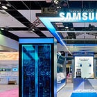
At FMS 2026, Samsung unveiled concept models for zHBM and zNAND-O, alongside its new 400-plus-layer V10 Bonding V-NAND.
在 FMS 2026 展會上,三星發表了 zHBM 與 zNAND-O 的概念模型,並同步推出全新的 400 多層 V10 鍵結 V-NAND。
8月5日8 月 5 日
The most radical concept was zHBM.
最大膽的概念是 zHBM。
Traditional HBM stacks sit beside an AI accelerator and connect through a high-density interposer or equivalent advanced packaging structure. Samsung’s zHBM concept moves toward vertically stacking HBM above the AI accelerator itself.
傳統的 HBM 堆疊位於 AI 加速器旁側,並透過高密度中介層或同等級的先進封裝結構進行連接。Samsung 的 zHBM 概念則朝向將 HBM 垂直堆疊於 AI 加速器正上方的方向發展。
The objective is to shorten the physical distance between compute and memory.
其目標在於縮短運算與記憶體之間的實體距離。
Samsung says a next-generation interface incorporating zHBM could eventually provide approximately eight times the performance of HBM5, more than 10 times its memory density, roughly three times the energy efficiency, and less than half the thermal resistance.
三星表示,整合 zHBM 的次世代介面,最終可提供約 HBM5 八倍的效能、超過十倍的記憶體密度、約三倍的能源效率,以及低於一半的熱阻。
These figures should be understood as Samsung’s concept-stage architectural targets—not current production specifications—but the strategic direction is more important than the exact numbers.
這些數據應理解為三星概念階段的架構目標,而非現行量產規格;但比起確切數字,其戰略方向更為重要。
Samsung is effectively arguing that the next step after conventional HBM may not simply be another faster HBM generation.
三星實質上主張,傳統 HBM 之後的下一步,未必只是推出另一代更快的 HBM。
It could be 3D memory-logic integration.
它可能是 3D 記憶體與邏輯的整合。
That changes the competitive landscape.
這改變了競爭格局。
Once memory begins moving vertically onto or extremely close to logic, memory design can no longer be separated cleanly from foundry technology, wafer bonding, thermal management, interface IP, power delivery and advanced packaging.
一旦記憶體開始垂直移動至邏輯晶片上或極其靠近的位置,記憶體設計便無法再與晶圓代工技術、晶圓鍵結、散熱管理、介面 IP、電源傳輸及先進封裝完全分離。
Samsung also said zHBM could support customer-specific designs, including customized IP integrated between the memory and AI accelerator.
三星亦表示,zHBM 可支援客戶專屬設計,包括整合於記憶體與 AI 加速器之間的客製化 IP。
This points toward another major structural change:
這指向另一項重大的結構性變革:
AI memory may become less standardized and more platform-specific.
AI 記憶體可能變得較少標準化,而更趨向平台專屬化。
That favors companies capable of co-designing compute, memory and packaging together.
這有利於能夠共同設計運算、記憶體與封裝的公司。
NAND Is Becoming an AI Technology Again
NAND 再次成為 AI 技術
Another important takeaway from FMS 2026 was the rehabilitation of NAND.
FMS 2026 的另一項重要收穫是 NAND 的復甦。
For years, NAND was viewed primarily through the cyclical economics of smartphones, PCs and storage.
多年來,NAND 主要被視為受智慧型手機、PC 與儲存裝置的週期性經濟所驅動。
AI is changing that narrative.
人工智慧(AI)正在改變此一敘事。
SK hynix unveiled its tenth-generation 375-layer 4D NAND, its first NAND generation using wafer bonding. The company says the technology improves performance per watt by 2.5 times versus the previous generation and plans to begin mass production of high-performance enterprise SSDs based on the architecture in the first half of 2027.
SK hynix 發表了其第十代 375 層 4D NAND,這是該公司首款採用晶圓接合(wafer bonding)技術的 NAND 世代。該公司表示,相較於前一代,此技術可將每瓦效能提升 2.5 倍,並計畫於 2027 年上半年開始量產基於此架構的高效能企業級 SSD。
Samsung presented a parallel direction.
三星則提出了平行的發展方向。
Its V10 Bonding V-NAND exceeds 400 layers and uses wafer bonding to separate and optimize the memory-cell and peripheral logic structures. Samsung says the architecture increases memory density by approximately 58% versus V9, while improving read, write and I/O performance.
其 V10 鍵結式 V-NAND 層數超過 400 層,並採用晶圓鍵結技術將記憶體單元與周邊邏輯結構分離並進行優化。三星表示,相較於 V9,此架構使記憶體密度提升約 58%,同時改善讀取、寫入及 I/O 效能。
Samsung also showed zNAND-O, a low-latency, high-I/O NAND architecture under development in four- and eight-layer configurations.
三星亦展示了 zNAND-O,這是一款正在開發中的低延遲、高 I/O NAND 架構,提供四層與八層配置。
Put these announcements together and the message is clear:
將這些公告綜合來看,訊息非常明確:
NAND vendors increasingly want flash to move upward in the AI memory hierarchy.
NAND 供應商日益希望快閃記憶體在 AI 記憶體階層中向上移動。
The AI storage market is therefore no longer just about selling larger SSDs.
因此,AI 儲存市場已不再只是銷售更大容量的 SSD。
It is becoming a competition around latency, bandwidth, proximity to compute, memory semantics and workload-aware data placement.
這正演變為一場圍繞延遲、頻寬、與運算單元的接近程度、記憶體語意以及工作負載感知資料放置的競爭。
Advanced Packaging Becomes Part of the Memory Architecture
先進封裝成為記憶體架構的一部分
All of this leads directly to advanced packaging.
所有這些都直接指向先進封裝。
As memory architectures become more heterogeneous, the importance of packaging rises.
隨著記憶體架構變得更加異質化,封裝的重要性也隨之提升。
HBM already demonstrated this.
HBM 已經證明了這一點。
But HBF, chiplets, CXL-attached accelerators, wafer-bonded NAND and vertically integrated zHBM could take the trend considerably further.
但 HBF、Chiplet、透過 CXL 連接的加速器、晶圓鍵結 NAND 以及垂直整合的 zHBM,可能會將此趨勢推向更遠。
Intel made essentially the same argument in late July when discussing Foveros, EMIB and EMIB-T. The company described AI systems as moving away from one massive die toward a “system of chips,” with specialized compute, memory and I/O tiles integrated through advanced packaging.
英特爾(Intel)在七月下旬討論 Foveros、EMIB 和 EMIB-T 時,也提出了 essentially 相同的論點。該公司描述 AI 系統正從單一大型晶片轉向「晶片系統」(system of chips),並透過先進封裝技術整合專用的運算、記憶體和 I/O 區塊。
Its latest EMIB-T architecture incorporates vertical power delivery through TSV-enabled bridges, improving signal routing and power delivery for systems incorporating technologies such as next-generation HBM.
其最新的 EMIB-T 架構透過支援 TSV 的橋接器實現垂直供電,改善了訊號路由與供電效率,適用於整合次世代 HBM 等技術的系統。
This is why advanced packaging should no longer be thought of as simply the semiconductor industry’s back-end manufacturing step.
這就是為什麼先進封裝不應再被視為半導體產業單純的後段製程步驟。
Packaging is becoming system architecture.
封裝正逐漸成為系統架構。
For the supply chain, that potentially increases the strategic importance of 2.5D and 3D integration, hybrid bonding, wafer bonding, ABF substrates, glass substrates, thermal interface materials, advanced cooling, precision bonding equipment, metrology and high-end testing.
對供應鏈而言,這可能提升 2.5D 與 3D 整合、混合鍵結、晶圓鍵結、ABF 基板、玻璃基板、熱介面材料、先進散熱技術、精密鍵結設備、量測以及高階測試的戰略重要性。
The bottleneck after HBM may therefore not be memory wafer capacity alone.
因此,HBM 之後的瓶頸可能不再僅是記憶體晶圓產能。
It could increasingly become the ability to assemble, power, cool and test highly heterogeneous memory-compute systems at acceptable yields.
它將日益取決於能否以可接受的良率,組裝、供電、散熱並測試高度異質的記憶體 - 運算系統。
Government Policy Is Moving in the Same Direction
政府政策正朝相同方向推進
The policy environment is beginning to reflect this architectural transition.
政策環境開始反映此架構轉型。
On July 29, the U.S. Department of Commerce announced letters of intent totaling US$874 million under CHIPS R&D programs covering integrated photonics, compute architecture, advanced packaging, substrates, materials and new memory technologies.
7 月 29 日,美國商務部宣布依據《晶片與科學法案》(CHIPS)研發計畫簽署意向書,總金額達 8.74 億美元,涵蓋整合光子學、運算架構、先進封裝、基板、材料以及新型記憶體技術。
Among the proposed investments are up to US$300 million for GlobalFoundries to accelerate co-packaged optics R&D, US$245 million for Kepler to develop new 3D and ferroelectric AI memory technology, and US$140 million for Multibeam to develop advanced packaging technologies. These remain letters of intent subject to additional diligence rather than final awards.
擬議的投資項目包括:撥款高達 3 億美元予 GlobalFoundries,以加速共封裝光學(co-packaged optics)的研發;撥款 2.45 億美元予 Kepler,用於開發新型 3D 及鐵電 AI 記憶體技術;以及撥款 1.4 億美元予 Multibeam,以發展先進封裝技術。這些目前仍屬意向書(letters of intent),須經進一步盡職調查,尚未成為最終獲獎項目。
The implication is important.
其影響至關重要。
Governments are increasingly recognizing that advanced AI competitiveness cannot be secured simply by building leading-edge transistor capacity.
各國政府日益體認到,僅靠建置先進製程的電晶體產能,已不足以確保在人工智慧領域的領先競爭力。
The strategic unit is becoming the compute supply chain itself.
戰略單位正逐漸轉向整個運算供應鏈本身。
Memory, packaging, substrates, photonics, materials and interconnects are all entering the policy equation.
記憶體、封裝、基板、光子學、材料與互連技術,皆已納入政策考量的關鍵方程式中。
Capital Spending Is Following the Architecture
資本支出正緊跟架構變革
Industry investment is moving in the same direction.
產業投資也正朝同一方向邁進。
On August 7, SK hynix approved approximately KRW54 trillion of investment for two new fabs: KRW35.2 trillion for the Yongin Y2 DRAM fab and KRW19.1 trillion for the Cheongju M17 NAND fab.
8 月 7 日,SK hynix 核准約 54 兆韓元的投資,用於興建兩座新晶圓廠:其中 35.2 兆韓元投入龍仁 Y2 DRAM 晶圓廠,19.1 兆韓元則用於清州 M17 NAND 晶圓廠。
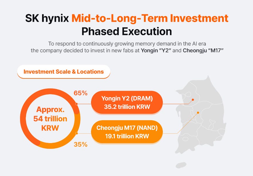
Y2 is intended to support next-generation DRAM including HBM, while M17 expands NAND production as enterprise SSD, KV-cache and AI-inference demand grows. The first cleanrooms are currently scheduled for December 2028 at M17 and June 2029 at Y2.
Y2 旨在支援包含 HBM 在內的次世代 DRAM,而隨著企業級 SSD、KV-cache 及 AI 推論需求成長,M17 將擴充 NAND 產能。首間無塵室預計於 2028 年 12 月在 M17 啟用,並於 2029 年 6 月在 Y2 啟用。
The timing is revealing.時機耐人尋味。
SK hynix unveiled an architecture spanning HBM, DRAM, HBF, NAND, SSD and CXL at FMS—and almost immediately committed massive capital to both DRAM and NAND infrastructure.
SK hynix 在 FMS 上發表了涵蓋 HBM、DRAM、HBF、NAND、SSD 和 CXL 的架構,並幾乎立即承諾投入巨額資本於 DRAM 和 NAND 基礎設施。
That suggests future capex should not be evaluated simply by asking:
這意味著未來的資本支出不應僅透過以下問題來評估:
How much wafer capacity is being added?
增加了多少晶圓產能?
A better question may be:
更恰當的問題可能是:
What part of the future AI memory hierarchy is that capacity intended to serve?
該容量旨在服務未來 AI 記憶體階層架構中的哪一部分?
Why This Matters for Taiwan
為何這對台灣至關重要
For Taiwan’s semiconductor supply chain, this transition could be particularly significant.
對台灣的半導體供應鏈而言,此項轉型可能尤為關鍵。
Taiwan’s advantage is not limited to advanced wafer fabrication. The ecosystem also spans advanced packaging and testing, substrates, PCB, thermal management, power delivery, system assembly and a large network of semiconductor equipment and materials suppliers.
台灣的優勢不僅限於先進晶圓製造,其生態系亦涵蓋先進封裝與測試、基板、印刷電路板(PCB)、散熱管理、電源供應、系統組裝,以及龐大的半導體設備與材料供應商網絡。
That becomes increasingly valuable when performance depends on integration across several layers of the stack.
當效能取決於跨越多層堆疊的整合時,其價值將日益顯著。
In the HBM era, the bottleneck was concentrated heavily around DRAM technology and advanced packaging capacity.
在 HBM 時代,瓶頸高度集中於 DRAM 技術與先進封裝產能。
In the Tiered Memory era, the opportunity set becomes wider.
在分層記憶體時代,機會範圍變得更為廣泛。
HBF requires NAND stacking, TSVs, logic dies and new interfaces.
HBF 需要 NAND 堆疊、TSV、邏輯晶粒以及新介面。
zHBM would require much more aggressive 3D integration, wafer bonding and thermal engineering.
zHBM 將需要更積極的 3D 整合、晶圓鍵結與熱工程技術。
Chiplet architectures increase requirements for advanced substrates and high-density interconnects.
小晶片(Chiplet)架構提高了對先進基板與高密度互連的需求。
CXL expands demand for controllers, switches, modules and system-level validation.
CXL 擴展了對控制器、交換器、模組及系統層級驗證的需求。
Higher-power packages create additional demand for cooling and power-management technologies.
高功率封裝創造了對散熱與電源管理技術的額外需求。
And increasingly complicated heterogeneous systems require more sophisticated testing.
日益複雜的異質系統則需要更精密的測試。
For Taiwan, therefore, the next AI memory cycle may not simply mean producing more components.
因此,對台灣而言,下一波 AI 記憶體週期可能不僅僅意味著生產更多元件。
The higher-value opportunity could be integrating more of the system.
更高價值的機會在於整合更多系統元件。
Five Signals to Watch Next
值得關注的五大訊號
The architecture is still evolving, and not every technology shown at FMS will reach volume production.
該架構仍在演進中,並非 FMS 展會上展示的每一項技術都能進入量產階段。
Five indicators will be particularly important.
有五項指標將尤為重要。
First, watch HBF ecosystem adoption.
首先,請關注 HBF 生態系的採用情況。
Google and Tenstorrent joining the consortium is meaningful, but the real inflection point would be public adoption by major hyperscalers, GPU platforms or custom AI accelerator vendors.
Google 和 Tenstorrent 加入聯盟具有重要意義,但真正的轉捩點將是主要超大型雲端服務商、GPU 平台或自訂 AI 加速器廠商的公開採用。
Second, watch CXL deployment at scale.
其次,關注 CXL 的大規模部署。
Technical demonstrations are no longer enough. Large production deployments of pooled memory for inference and KV-cache management would validate the Tiered Memory thesis.
技術示範已不再足夠。針對推論與 KV-cache 管理進行大規模生產部署的池化記憶體,將能驗證分層記憶體(Tiered Memory)的論點。
Third, watch zHBM’s commercialization roadmap.
第三,關注 zHBM 的商業化路線圖。
Customer validation, manufacturing partners, bonding technology, thermal architecture and production timing will determine whether Samsung’s concept begins influencing supply-chain investment several years before volume production.
客戶驗證、製造夥伴、接合技術、散熱架構與量產時程,將決定三星的構想是否會在量產前數年便開始影響供應鏈投資。
Fourth, watch packaging capacity, yields and lead times.
第四,關注封裝產能、良率與交貨週期。
If AI memory architectures become increasingly heterogeneous, advanced packaging could again become the limiting factor—even when sufficient DRAM and NAND wafers are available.
若 AI 記憶體架構日益異質化,先進封裝可能再次成為瓶頸因素——即使 DRAM 與 NAND 晶圓供應充足亦然。
Fifth, watch where capex and government funding move.
第五,關注資本支出與政府資金的流向。
If investment continues shifting toward advanced packaging, substrates, photonics, memory interconnects and heterogeneous integration, it will confirm that the industry increasingly views post-Moore system integration as a strategic asset.
若投資持續轉向先進封裝、基板、光子學、記憶體互連及異質整合,將證實產業界日益將後摩爾時代的系統整合視為戰略資產。
The Next Memory War Is About Architecture
下一場記憶體戰爭關乎架構
The semiconductor industry’s next AI memory battle is therefore not really about whether HBM remains important.
因此,半導體產業下一場 AI 記憶體之戰,關鍵並非在於 HBM 是否仍然重要。
It unquestionably does.毫無疑問,確實如此。
The more important development is that HBM is becoming one layer inside a much larger memory architecture.
更重要的發展是,HBM 正成為更大規模記憶體架構中的一個層級。
At one extreme, Samsung wants to bring memory closer to compute through zHBM and 3D memory-logic integration.
在一端,Samsung 希望透過 zHBM 與 3D 記憶體 - 邏輯整合技術,將記憶體更靠近運算單元。
At another, SK hynix, Sandisk and the broader ecosystem are trying to create new capacity tiers through HBF, NAND and CXL.
在另一端,SK hynix、Sandisk 及更廣泛的生態系則正致力於透過 HBF、NAND 和 CXL 建立新的容量層級。
Between them sits an increasingly complex combination of server DRAM, SOCAMM, enterprise SSDs, pooled memory, chiplets and workload-aware software.
介於兩者之間的,是日益複雜的組合,包括伺服器 DRAM、SOCAMM、企業級 SSD、記憶體池化、小晶片(chiplets)以及感知工作負載的軟體。
This is not simply another memory product cycle.
這不僅僅是另一個記憶體產品週期。
It represents a redefinition of where “memory” ends and where “compute,” “storage” and “packaging” begin.
這代表著對「記憶體」終點,以及「運算」、「儲存」與「封裝」起點的重新定義。
The extraordinary growth of the semiconductor market provides the economic backdrop. SIA reported global semiconductor sales of US$403.3 billion in Q2 2026, up 35.1% sequentially, while June sales reached US$134.5 billion, up 123.6% year over year.
半導體市場的驚人成長提供了經濟背景。SIA 報告指出,2026 年第二季全球半導體銷售額達 4,033 億美元,季增 35.1%;而 6 月銷售額更達 1,345 億美元,年增 123.6%。
The industry is therefore no longer asking whether AI demand exists.
因此,產業界已不再質疑 AI 需求是否存在。
It is asking which part of the infrastructure will become the next bottleneck.
現在的問題是:基礎設施的哪一部分將成為下一個瓶頸。
FMS 2026 provided an increasingly clear answer:
FMS 2026 提供了愈發清晰的答案:
The next AI memory war will not be won by HBM alone. It will be won by whoever can orchestrate HBM, DRAM, NAND, CXL, packaging, thermal management and compute into the most efficient architecture.
下一場 AI 記憶體之戰不會僅由 HBM 勝出。勝出者將是能夠將 HBM、DRAM、NAND、CXL、封裝、散熱管理與運算整合為最高效架構的一方。
For investors, that is a much larger story than a single memory generation.
對投資人而言,這遠比單一記憶體世代的更迭更為重大。
And for the semiconductor supply chain, it means the opportunity is spreading outward—from a handful of HBM leaders toward packaging, materials, substrates, controllers, testing, cooling, interconnects and system design.
對半導體供應鏈而言,這意味著機會正向外擴散——從少數 HBM 領導廠商,延伸至封裝、材料、基板、控制器、測試、散熱、互連技術與系統設計等領域。
HBM is still at the center of AI computing.
HBM 仍是 AI 運算的核心。
But the next battlefield is already taking shape around what comes after HBM.
但下一場戰役的輪廓,已圍繞著 HBM 之後的技術發展逐漸成形。
SEMIVISION @_@ 是一份由讀者支持的出版物。若要接收最新文章並支持我的工作,歡迎考慮成為免費或付費訂閱者。
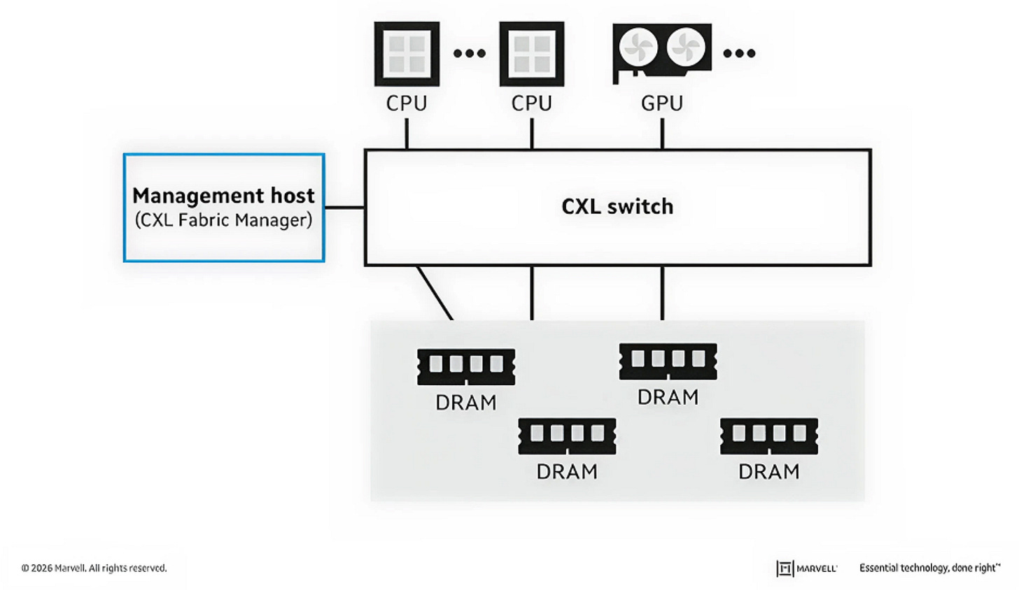
Memory is the second largest semiconductor cost in the data center, and the gap between what AI infrastructure needs and what conventional architectures can deliver is widening fast.
記憶體是資料中心中第二大半導體成本,而人工智慧基礎設施的需求與傳統架構所能提供的效能之間的差距正迅速擴大。
Marvell explains how the Structera S family of CXL switches addresses the AI memory wall by enabling terabytes of shareable, dynamically allocated memory across CPUs, GPUs and XPUs. The article covers real-world performance results, including a 4.8x improvement in inference throughput and an 82.7% reduction in time to first token, and introduces Structera S 30260, which supports up to 48TB of shared memory and 4TB per second of cumulative bandwidth. It also outlines how Structera S fits within a broader CXL portfolio spanning memory expansion, acceleration and pooling, the only such complete portfolio in the industry.
Marvell 說明 Structera S 系列 CXL 交換器如何透過在 CPU、GPU 與 XPU 之間提供可共享且動態配置的 TB 級記憶體,解決 AI 記憶體瓶頸。本文涵蓋實際效能成果,包括推論吞吐量提升 4.8 倍,以及首個 token 生成時間減少 82.7%,並介紹支援高達 48TB 共享記憶體與每秒 4TB 累積頻寬的 Structera S 30260。文章亦闡述 Structera S 如何融入更廣泛的 CXL 產品組合,涵蓋記憶體擴充、加速與資源池化,成為業界唯一具備完整解決方案的产品線。
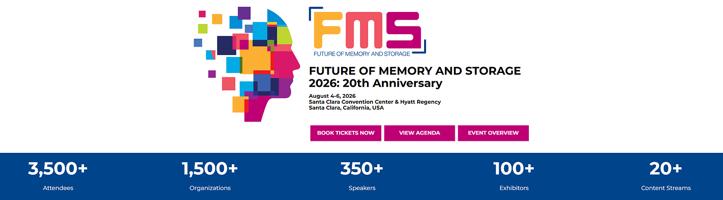
FMS 2026 Storage Summit: Four Key Takeaways
FMS 2026 儲存高峰會:四大關鍵重點
-
HBF Makes Its Standards Debut
-
HBF 正式亮相標準舞臺
HBF is emerging as a new high-bandwidth memory tier alongside HBM4.
HBF 正成為與 HBM4 並列的新高頻寬記憶體層級。
Stacking:8-high / 16-high
堆疊:8 層 / 16 層
Capacity:Up to 512GB per device
容量:每裝置最高可達 512GB
Bandwidth:0.4–3.0 TB/s頻寬:0.4–3.0 TB/s
Positioning:HBF is designed to complement, rather than directly replace, HBM.
定位:HBF 旨在互補而非直接取代 HBM。
HBF’s upper bandwidth range is beginning to approach HBM-class territory. Instead of a winner-takes-all replacement cycle, HBM and HBF could coexist at different levels of the AI memory hierarchy, balancing bandwidth, capacity and cost.
HBF 的頻寬上限已開始逼近 HBM 等級。與其進入贏家通吃的取代週期,HBM 與 HBF 更可能在 AI 記憶體層級架構的不同層級中共存,以平衡頻寬、容量與成本。
-
Samsung Moves Beyond 400-Layer NAND
-
三星突破 400 層 NAND 技術
Samsung introduced a new 400+ layer V10 BV-NAND architecture featuring wafer bonding.
三星推出採用晶圓鍵結技術的全新 400 層以上 V10 BV-NAND 架構。
Product:V10 BV-NAND產品:V10 BV-NAND
Layers:400+層數:400+
Process:Wafer bonding製程:晶圓鍵結
Two wafers are bonded face-to-face to optimize the memory and peripheral structures.
兩片晶圓以面對面方式鍵結,以最佳化記憶體與周邊結構。
Samsung also previewed zHBM and zNAND-O, which remain concept-stage technologies rather than mass-production products.
三星亦展示了 zHBM 與 zNAND-O,這些目前仍屬概念階段技術,尚未進入量產。
Key takeaway:關鍵要點:
The NAND race is moving beyond simply “who can stack more layers.”
NAND 競賽已不再只是「誰能堆疊更多層數」。
The next battleground is increasingly about process architecture, wafer bonding, performance, power efficiency and system integration.
下一個戰場將日益聚焦於製程架構、晶圓接合、效能、電源效率與系統整合。
-
Liquid Cooling Reaches Enterprise SSDs
-
液冷技術延伸至企業級 SSD
For the first time, liquid cooling is moving directly into the enterprise SSD architecture.
液冷技術首次直接導入企業級 SSD 架構。
Interface:PCIe 6.0介面:PCIe 6.0
NAND:332-layer BiCS10NAND:332 層 BiCS10
Cooling:Direct cold-plate liquid cooling
散熱:直接冷板式液冷
Application:Enterprise/data-center SSDs
應用:企業級/資料中心 SSD
As PCIe speeds and NAND performance increase, SSD power density and thermal requirements are also rising. The data-center cooling problem is no longer confined to GPUs and AI accelerators.
隨著 PCIe 速度與 NAND 效能提升,SSD 的功率密度與散熱需求也隨之增加。資料中心的散熱問題已不再限於 GPU 與 AI 加速器。
The thermal budget is now expanding into the storage layer. This could create new opportunities across SSD thermal design, cold plates, liquid-cooling infrastructure and data-center thermal management.
散熱預算現已擴展至儲存層。這將為 SSD 散熱設計、冷板、液冷基礎設施以及資料中心熱管理帶來新的機會。
-
Memory Capacity Expansion Is Accelerating Aggressively
-
記憶體容量擴張正加速推進
The memory industry is entering another major capacity-expansion cycle.
記憶體產業正進入另一輪大規模產能擴張週期。
Current Samsung HBM capacity:~170K wafers/month
目前三星 HBM 產能:~170K 晶圓/月
Target by end-2026:~250K wafers/month
2026 年底目標:每月 25 萬片晶圓
Increase:approximately +47%
增長:約 +47%
SK hynix:Continuing aggressive investment and capacity expansion
SK hynix:持續積極投資並擴大產能
Samsung, SK hynix and Micron:All expanding simultaneously
Samsung、SK hynix 與 Micron:三者同步擴產
The synchronized expansion by all three major memory suppliers shows that AI-driven demand has been strong enough to justify another major investment cycle.
三大記憶體供應商同步擴產,顯示 AI 驅動的 demand 已強勁到足以支撐新一輪大規模投資週期。
At the same time, synchronized capacity expansion is also a reminder that memory remains a cyclical industry.
與此同時,產能的同步擴張也提醒我們,記憶體產業仍具有週期性。
The important question for 2027–2028 will therefore shift from:
因此,2027 至 2028 年的關鍵問題將從:
“Is there enough HBM?”「HBM 產能是否足夠?」
to:轉變為:
“How quickly can new capacity come online, and will AI demand continue absorbing it?”
新產能能以多快速度上線,而 AI 需求是否將持續吸收這些產能?
FMS 2026 in One Sentence
一句話總結 FMS 2026
The memory industry is moving from an HBM-centric cycle toward a broader AI memory architecture—combining HBM, HBF, advanced NAND, liquid-cooled storage, wafer bonding and massive capacity expansion.
記憶體產業正從以 HBM 為核心的週期,轉向更廣泛的 AI 記憶體架構——結合 HBM、HBF、先進 NAND、液冷儲存、晶圓鍵結與大規模產能擴張。
Thanks for reading SEMIVISION @_@! This post is public so feel free to share it.
感謝閱讀 SEMIVISION @_@!本文為公開文章,歡迎自由分享。


Share分享
Previous上一頁