No InP, No Optical Transceiver ?!
No InP, No Optical Transceiver ?!
- Source: SemiVision
- Author: SEMIVISION
- Published: 2026-08-07T11:43:09+08:00
- URL: https://tspasemiconductor.substack.com/p/no-inp-no-optical-transceiver
中文翻譯與英文原文(雙語)
沒有 InP,就沒有光學收發器?!- SEMIVISION @@ --- No InP, No Optical Transceiver ?! - SEMIVISION @@


No InP, No Optical Transceiver ?!
沒有 InP,就沒有光學收發器?!
Original Article By SemiVision Research [Reading time: 7 mins]
原文作者:SemiVision Research [閱讀時間:7 分鐘]

Aug 07, 2026
∙ Paid∙ 付費
Share分享
No InP, No Optical Transceiver ?!
沒有 InP,就沒有光學收發器?!

The artificial-intelligence infrastructure boom is creating a new semiconductor bottleneck, but it is not located inside the GPU.
人工智慧基礎設施的蓬勃發展正引發新的半導體瓶頸,但此瓶頸並非位於 GPU 內部。
It is located inside the optical link.
而是存在於光學連結之中。
As AI clusters expand from thousands to hundreds of thousands of accelerators, data must move rapidly between GPUs, switches, racks and eventually entire data-center campuses. Copper connections are increasingly constrained by reach, signal integrity and power consumption. Optical interconnects are therefore moving closer to the processor, from conventional pluggable transceivers toward near-packaged optics and co-packaged optics.
隨著 AI 叢集規模從數千個加速器擴展至數十萬個,資料必須在 GPU、交換器、機架乃至整個資料中心園區之間快速傳輸。銅線連接日益受到傳輸距離、訊號完整性及功耗的限制。因此,光學互連技術正不斷靠近處理器,從傳統的可插拔收發器朝向近封裝光學與共封裝光學演進。
Yet every optical network requires a source of light. Silicon can route, split and modulate light, but conventional silicon is an inefficient light emitter because of its indirect bandgap. Direct-bandgap III-V materials, especially indium phosphide, remain the commercially established solution for generating and detecting light at the wavelengths used in high-speed data-center communications.
然而,每套光網路皆需光源。矽雖能導引、分光與調變光訊號,但因其間接能隙特性,傳統矽作為發光元件效率極低。直接能隙的 III-V 族材料,尤其是磷化銦(InP),仍是目前商業上用於產生與偵測高速資料中心通訊所需波長光訊號的成熟解決方案。
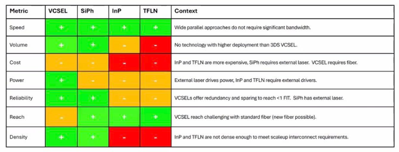
Strictly speaking, “No InP, no optical transceiver” is an industry shorthand rather than a universal scientific rule. Some short-reach multimode transceivers use gallium-arsenide VCSELs.
嚴格來說,「沒有 InP 就沒有光學收發器」是業界的一種簡化說法,而非普遍的科學法則。某些短距離多模收發器使用的是砷化鎵 VCSEL。
Source: Lumentum來源:Lumentum
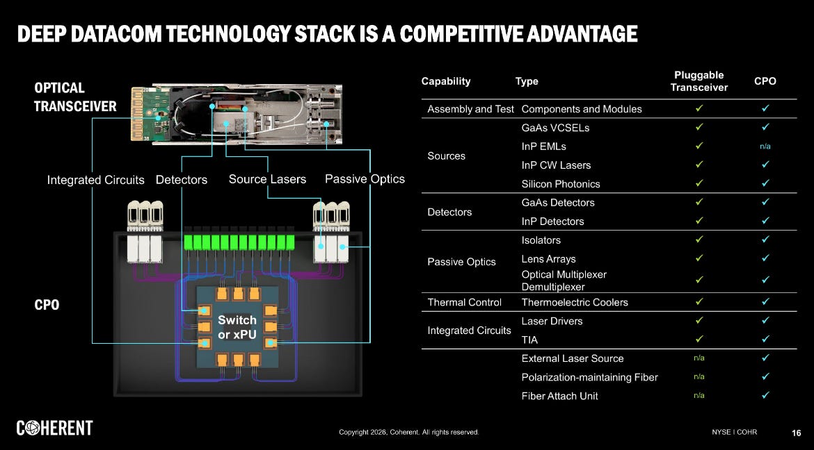
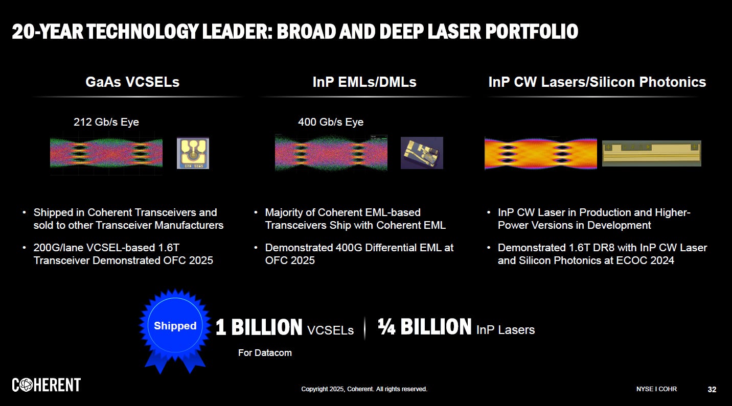
But for the high-speed single-mode links increasingly used in 800G, 1.6T and future 3.2T systems, InP-based EMLs, continuous-wave lasers and photodetectors have become foundational components. Coherent’s current product roadmap, for example, combines InP EMLs for pluggable modules, high-power InP CW lasers for silicon-photonics transceivers and CPO, and InP photodiodes for receiving optical signals.
但對於日益應用於 800G、1.6T 及未來 3.2T 系統的高速單模鏈路而言,基於 InP 的 EML、連續波雷射與光偵測器已成為基礎元件。以 Coherent 目前的產品路線圖為例,其結合了用於可插拔模組的 InP EML、用於矽光子收發器與 CPO 的高功率 InP 連續波雷射,以及用於接收光訊號的 InP 光二極體。
Below we will share:以下我們將分享:
Where InP Capacity Is Expanding
InP 產能擴張之地
Supply-Chain Outlook供應鏈展望
3月26日3 月 26 日
2025年6月16日2025 年 6 月 16 日
2025年5月15日2025 年 5 月 15 日
SemiAnalysis: InP Is Gating the AI Buildout
SemiAnalysis:InP 正制約 AI 基礎建設的擴展
SemiAnalysis has framed the problem clearly. Konrad Wang, a research analyst at the firm, described InP as “one of several supply chain bottlenecks collectively gating AI data centre buildouts.”
SemiAnalysis 已清楚闡述此問題。該公司的研究分析師 Konrad Wang 將 InP 描述為「共同制約 AI 資料中心擴建的供應鏈瓶頸之一」。
The important word is collectively. AI infrastructure is not limited by one component. GPUs depend on HBM, advanced packaging, power delivery, cooling, networking and data-center electricity. Within networking, the optical supply chain is itself dependent on several tightly connected layers: indium feedstock, InP crystal growth, polished substrates, epitaxial wafers, laser fabrication, device packaging, optical-engine assembly and final transceiver production.
關鍵詞是「整體性」。AI 基礎設施並非受限於單一元件。GPU 依賴高頻寬記憶體(HBM)、先進封裝、電源供應、散熱、網路連線以及資料中心的電力。在網路層面,光學供應鏈本身又取決於數個緊密相連的環節:銦原料、磷化銦(InP)晶體生長、拋光基板、磊晶晶圓、雷射製造、元件封裝、光引擎組裝,乃至最終的光收發模組生產。
A disruption at the substrate level can therefore propagate through epitaxy suppliers, laser manufacturers and optical-module companies. SemiAnalysis also noted that Taiwanese suppliers including VPEC and LandMark Optoelectronics had experienced substrate disruption related to delays in export permits for AXT’s China-produced InP wafers.
因此,基板層級的斷鏈可能會連鎖影響磊晶供應商、雷射製造商以及光模組廠商。SemiAnalysis 亦指出,包括聯亞光電(VPEC)與凌陽光電(LandMark Optoelectronics)在內的台灣供應商,曾因 AXT 於中國生產之 InP 晶圓出口許可延宕,而遭遇基板供應中斷的問題。
This is why the present shortage is more complicated than simply building another optical-module assembly line.
這正是當前短缺問題比單純增設一條光模組組裝產線更為複雜的原因所在。

3月14日3 月 14 日
Silicon Photonics Still Needs a Light Source
矽光子技術仍需光源
Silicon photonics is frequently described as the technology that will replace conventional optical components. That description is incomplete.
矽光子技術常被描述為將取代傳統光學元件的技術。然而,此描述並不完整。
Silicon photonics can integrate waveguides, modulators, multiplexers and other optical functions using semiconductor manufacturing methods. However, it still generally requires a III-V light source. That light source may be attached as a discrete laser, integrated as a laser chiplet, bonded to the silicon-photonics die or placed outside the package in an external laser source.
矽光子技術可利用半導體製程整合波導、調變器、多工器及其他光學功能。然而,它通常仍需要 III-V 族材料光源。該光源可作為離散雷射附加、整合為雷射小晶片(chiplet)、鍵結至矽光子晶粒,或置於封裝外部作為外部雷射光源。
In many of these architectures, the actual laser remains InP-based.
在許多此類架構中,實際的雷射光源仍基於磷化銦(InP)。
The transition to CPO does not eliminate InP demand. It changes the type of InP device required. Conventional transceivers may use directly modulated lasers or electro-absorption modulated lasers. Silicon-photonics transceivers and CPO systems increasingly use continuous-wave DFB lasers, including higher-power versions capable of feeding multiple optical channels.
轉向共封裝光學(CPO)並未消除對 InP 的需求,而是改變了所需 InP 元件的類型。傳統收發器可能使用直接調變雷射或電吸收調變雷射;而矽光子收發器與 CPO 系統則日益採用連續波 DFB 雷射,包括能夠供應多個光通道的高功率版本。
Coherent is already producing 400-milliwatt InP lasers for CPO applications. Its CPO demonstrations combine silicon-photonics optical engines with external laser-source modules powered by high-power InP CW lasers.
Coherent 已開始為 CPO 應用生產 400 毫瓦的 InP 雷射。其 CPO 示範方案結合了矽光子光引擎與外部雷射源模組,後者由高功率 InP 連續波(CW)雷射驅動。
Nvidia’s move into silicon-photonics networking therefore does not remove the laser bottleneck. It brings the laser closer to the center of the AI system architecture. Nvidia says its CPO switches provide substantially improved power efficiency and network resilience compared with equivalent pluggable configurations, with product availability scheduled for the second half of 2026.
因此,Nvidia 進軍矽光子網路並未消除雷射瓶頸,而是將雷射更貼近 AI 系統架構的核心。Nvidia 表示,其 CPO 交換器與同等可插拔組態相比,能顯著提升電源效率與網路韌性,預計於 2026 年下半年開始供貨。
Where InP Capacity Is Expanding
磷化銦(InP)產能擴張現況
The industry has now started a global capacity race covering substrates, six-inch wafer processing and high-power laser production.
產業界已展開一場涵蓋基板、六吋晶圓製程與高功率雷射生產的全球產能競賽。
Coherent: Sherman, Järfälla and Zurich
Coherent:Sherman、Järfälla 與 Zurich
Coherent currently operates InP production sites in Fremont, California; Sherman, Texas; Järfälla, Sweden; and Zurich, Switzerland. Fremont continues to use three-inch production lines, while Sherman and Järfälla operate six-inch InP lines. Zurich is being converted from its GaAs heritage into Coherent’s newest six-inch InP facility.
Coherent 目前於加州佛利蒙(Fremont)、德州謝爾曼(Sherman)、瑞典賈法拉(Järfälla)及瑞士蘇黎世(Zurich)營運磷化銦(InP)生產據點。佛利蒙廠區仍使用三吋生產線,而謝爾曼與賈法拉則營運六吋 InP 產線。蘇黎世廠區正從其砷化鎵(GaAs)傳統產線轉型為 Coherent 最新的六吋 InP 設施。

Coherent expects its total InP output capacity to double during 2026 and rise to more than twice the 2026 level by the end of 2027. The company is ramping six-inch capacity in Texas and Sweden while adding new six-inch capacity in Switzerland. It also says six-inch InP manufacturing is producing better yields than its traditional three-inch process.
Coherent 預期其磷化銦(InP)總產能將於 2026 年翻倍,並在 2027 年底前進一步提升至超過 2026 年水準的兩倍。該公司正於美國德州與瑞典擴增六吋產能,同時在瑞士新增六吋產能。Coherent 亦表示,六吋 InP 製程的良率優於其傳統的三吋製程。
The Sherman site is the centerpiece. Coherent plans to double the facility’s manufacturing space and quadruple wafer-production capacity. The project has received a letter of intent for up to US$50 million in U.S. CHIPS Act support, in addition to approximately US$20 million previously committed by Texas and local economic-development agencies.
謝爾曼廠區是整個計畫的核心。Coherent 計劃將該廠區的製造空間擴大一倍,並將晶圓產能提升為原來的四倍。此專案已獲得美國《晶片法案》最高達 5,000 萬美元的意向書支持,此外還包括德克薩斯州及當地經濟發展機構先前承諾的約 2,000 萬美元資金。
Lumentum: A New Six-Inch Fab in Greensboro
Lumentum:格林斯伯勒的全新六吋晶圓廠
Lumentum is establishing a 240,000-square-foot InP manufacturing facility in Greensboro, North Carolina, using a former Qorvo semiconductor plant. The site will be retrofitted for six-inch InP production, including CW and ultra-high-power lasers used in AI optical networks.
Lumentum 正在北卡羅來納州格林斯伯勒建立一座面積達 24 萬平方英尺的磷化銦(InP)製造設施,該設施將利用前 Qorvo 半導體廠房進行改造。此廠區將改裝用於六吋 InP 生產,涵蓋應用於 AI 光學網路的連續波(CW)雷射與超高功率雷射。

The company plans to invest hundreds of millions of dollars and preserve or create more than 400 manufacturing jobs. Production is expected to begin ramping in mid-2028.
該公司計劃投資數億美元,並保留或創造超過 400 個製造業就業機會。預計生產將於 2028 年年中開始逐步提升產量。
Nvidia has separately agreed to invest US$2 billion in Lumentum, accompanied by multiyear purchasing commitments and future capacity-access rights. Nvidia also announced a US$2 billion investment and strategic capacity agreement with Coherent. These transactions show that laser supply is no longer being treated as an ordinary component-procurement issue. Hyperscale customers are directly financing capacity to secure future optical infrastructure.
Nvidia 已另行同意向 Lumentum 投資 20 億美元,並伴隨多年期採購承諾與未來產能取得權。Nvidia 亦宣布對 Coherent 進行 20 億美元投資並簽訂戰略產能協議。這些交易顯示,雷射供應已不再被視為一般的元件採購議題;超大型雲端服務業者正直接資助產能擴建,以確保未來光學基礎設施的穩定供貨。
Even with ongoing expansion, Reuters reported that Lumentum’s available capacity was effectively committed through 2028.
即使持續擴產,路透社報導指出,Lumentum 的可用產能實際上已預訂至 2028 年。

4月12日4 月 12 日
JX Advanced Metals: Isohara and Hitachinaka
JX Advanced Metals:磯原與日立那珂
The most aggressive substrate expansion may be taking place in Japan.
最積極的基板擴產行動可能正在日本展開。
JX Advanced Metals plans to invest up to ¥120 billion over four years in InP substrates. In addition to its existing Isohara Works in Kitaibaraki, Ibaraki Prefecture, the company will establish additional production capacity in the Hitachinaka area.
JX Advanced Metals 計劃在四年內投資高達 1,200 億日圓於磷化銦(InP)基板。除了位於茨城縣北茨城市的現有磯原工廠外,該公司還將在日立那珂地區建立額外的產能。

JX expects the combined program to increase its InP substrate capacity by approximately seven to ten times. Including previously announced projects, its cumulative InP-related investment is expected to reach roughly ¥150 billion.
JX 預期該綜合計畫將使其磷化銦(InP)基板產能提升約七至十倍。若計入先前已宣布的專案,其累計與 InP 相關的投資金額預計將達約 1,500 億日圓。
This expansion is particularly important because substrates sit upstream of both epitaxy and laser fabrication. Adding MOCVD tools or laser-processing capacity does not solve the problem when qualified substrates remain unavailable.
此項擴產至關重要,因為基板位於磊晶與雷射製造的上游。若合格基板仍供不應求,僅增加 MOCVD 設備或雷射加工產能並無法解決問題。
Sumitomo Electric: Itami Works
住友電氣工業:伊丹製作所
住友電氣工業亦正加大對磷化銦(InP)基板的投資。據報導,該公司計劃投入約 180 億日圓,用於升級其位於兵庫縣伊丹製作所的生產設施。
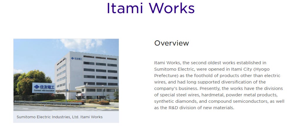
目標是到 2028 財年將產能提升至 2024 財年水準的約 3.1 倍,高於先前的擴產目標。與新建晶圓廠不同,此專案將升級現有生產線,應可讓產能更快投入量產。
Sumitomo is strategically important because it is both a major substrate supplier and a producer of optical devices. However, a meaningful portion of its substrate output is reportedly consumed internally, limiting how much supply becomes available to independent epitaxy and laser companies.
住友電工具有戰略重要性,因為它既是主要的基板供應商,也是光學元件製造商。然而,據報導其相當一部分的基板產量供內部使用,限制了可供應給獨立磊晶與雷射廠商的數量。
China: Capacity Is Growing, but Export Availability Is Uncertain
中國:產能持續成長,但出口供應仍具不確定性
Chinese companies are also expanding. Yunnan Germanium announced a RMB189 million investment intended to lift annual production capacity to approximately 450,000 InP substrates. Guangdong Xianrui, controlled by Guangdong Xiandao, has launched a project targeting annual production of 40 tonnes of InP crystal material.
中國企業亦正積極擴產。雲南鍺業宣布投資人民幣 1.89 億元,旨在將年產能提升至約 45 萬片磷化銦(InP)基板。由廣東先导控制的廣東先瑞已啟動一項專案,目標為年產 40 噸磷化銦(InP)晶體材料。

However, new Chinese capacity does not necessarily translate into internationally available supply. Export licensing, customer qualification and geopolitical restrictions remain major variables. Optical-device manufacturers cannot rapidly substitute one substrate supplier for another because changes in crystal quality, defect density and wafer specifications can require lengthy requalification.
然而,中國新增的產能未必能轉化為國際市場上的可用供應。出口許可、客戶認證以及地緣政治限制仍是主要變數。光學元件製造商無法迅速替換基板供應商,因為晶體品質、缺陷密度及晶圓規格的變更可能需要耗時長久的重新認證程序。
Expansion Is Also Moving Downstream
擴張也正向下游推進
Module and component assembly capacity is expanding as well. Innolight has built a major offshore manufacturing base in Thailand to support optical-transceiver production and reduce geographic concentration. Fabrinet is expanding in Chonburi, Thailand, where its Building 10 project is designed to add roughly two million square feet of manufacturing space and several billion dollars of potential revenue capacity.
模組與元件組裝產能亦持續擴增。中際旭創(Innolight)已在泰國建立大型海外製造基地,以支援光學收發器生產並降低地理集中風險。Fabrinet 則於泰國春武里府擴大佈局,其「10 號廠房」專案預計新增約二百萬平方英呎的製造空間,並帶來數十億美元的潛在營收產能。
LiteOn has invested US$34.3 million for approximately 21% of Singapore-based DenseLight, an InP photonics IDM producing CW DFB lasers, gain chips and semiconductor optical amplifiers. The investment gives Lite-On a more direct position upstream of its future optical-module and rack-scale interconnect business.
光寶科技已投資 3,430 萬美元,取得新加坡 DenseLight 約 21% 的股權。DenseLight 是一家磷化銦(InP)光子學整合元件製造商(IDM),生產連續波分佈回饋式(CW DFB)雷射、增益晶片及半導體光放大器。此項投資使光寶科技在其未來的光模組與機架級互連業務中,獲得更直接的上游佈局優勢。
But these downstream expansions reinforce the central issue: optical-module factories can be built faster than qualified InP substrate, epitaxy and laser capacity.
但這些下游擴產反而凸顯了核心問題:光模組工廠的建置速度,遠快於合格的磷化銦(InP)基板、磊晶與雷射產能的提升速度。
Supply-Chain Outlook供應鏈展望
The InP shortage is unlikely to be solved by one investment cycle.
磷化銦(InP)的短缺問題不太可能透過單一投資週期就獲得解決。
Coherent’s six-inch transition should deliver meaningful output and yield improvement during 2026 and 2027. JX, Sumitomo and Chinese substrate producers are also adding capacity. But Lumentum’s Greensboro facility will not begin ramping until 2028, and substrate projects must still complete crystal-growth stabilization, wafer processing and customer qualification.
Coherent 轉向六吋晶圓的製程,預計將在 2026 至 2027 年間帶來顯著的產出與良率提升。JX、Sumitomo 以及中國的基板製造商也紛紛擴增產能。然而,Lumentum 位於 Greensboro 的廠區要到 2028 年才會開始量產,且各項基板專案仍須完成晶體生長穩定化、晶圓加工以及客戶認證等階段。
The market should therefore distinguish between announced capacity, installed capacity, qualified capacity and available capacity. These are not the same thing.
因此,市場應清楚區分「已宣布產能」、「已安裝產能」、「已認證產能」與「可用產能」。這些概念並不相同。
The most important supply-chain indicators are now six-inch InP substrate availability, MOCVD tool additions, EML and CW-laser yields, high-power laser reliability, external-laser packaging capacity and customer qualification progress. For CPO, thermal stability and optical coupling will become as important as raw wafer output.
目前最重要的供應鏈指標包括六吋磷化銦(InP)基板供應、MOCVD 設備增設、EML 與連續波(CW)雷射良率、高功率雷射可靠性、外部雷射封裝產能,以及客戶認證進度。就共封裝光學(CPO)而言,熱穩定性與光耦合效率將變得與晶圓產出量同等重要。
The broader conclusion is straightforward:
更廣泛的結論十分明確:
AI infrastructure is moving from an era dominated by compute-chip procurement into one governed by system-level constraints. HBM determines whether accelerators can process data. Advanced packaging determines whether processors and memory can be integrated. Power and cooling determine whether the racks can operate.
AI 基礎設施正從以運算晶片採購為主的時代,邁入受系統層級限制所主導的新階段。HBM 決定了加速器能否處理資料;先進封裝決定了處理器與記憶體能否整合;電力與散熱則決定了機櫃能否正常運作。
And InP determines whether those racks can communicate at scale.
而磷化銦(InP)決定了這些機櫃能否實現大規模通訊。
No InP, no light. No light, no scalable AI network.
沒有 InP,就沒有光。沒有光,就無法建構可擴展的 AI 網路。
Thanks for reading SEMIVISION @_@! This post is public so feel free to share it.
感謝閱讀 SEMIVISION @_@!本文為公開文章,歡迎自由分享。


Share分享
Previous上一頁