Samsung’s zHBM & zNAND Signals a New Era of 3D AI Chip Architecture
Samsung’s zHBM & zNAND Signals a New Era of 3D AI Chip Architecture
- Source: SemiVision
- Author: SEMIVISION
- Published: 2026-08-05T10:12:48+08:00
- URL: https://tspasemiconductor.substack.com/p/samsungs-zhbm-and-znand-signals-a
中文翻譯與英文原文(雙語)
三星 zHBM 與 zNAND 標誌著 3D AI 晶片架構的新紀元 --- Samsung’s zHBM & zNAND Signals a New Era of 3D AI Chip Architecture


Samsung’s zHBM & zNAND Signals a New Era of 3D AI Chip Architecture
三星 zHBM 與 zNAND 標誌著 3D AI 晶片架構的新紀元
Original Article By SemiVision Research [Reading time: 12 mins]
原文作者:SemiVision Research [閱讀時間:12 分鐘]

Aug 05, 2026
∙ Paid∙ 付費
Share分享
Samsung’s zHBM & zNAND Signals a New Era of 3D AI Chip Architecture
三星 zHBM 與 zNAND 標誌著 3D AI 晶片架構的新時代

Samsung used FMS 2026 to introduce three important technology directions: zHBM, zNAND-O, and its 400-plus-layer V10 BV-NAND.
三星於 FMS 2026 大會上發表了三大重要技術方向:zHBM、zNAND-O,以及其超過 400 層的 V10 BV-NAND。
The most consequential announcement was zHBM, a concept architecture that places high-bandwidth memory vertically above an AI accelerator rather than positioning the memory stacks beside the processor. Samsung argues that the architecture could substantially shorten data-transfer distances while improving bandwidth, energy efficiency, memory density, and thermal performance.
最具影響力的發表是 zHBM,這是一種概念架構,將高頻寬記憶體垂直置於 AI 加速器上方,而非將記憶體堆疊放置於處理器旁側。三星主張,此架構可大幅縮短資料傳輸距離,同時提升頻寬、能源效率、記憶體密度與散熱效能。
The significance extends far beyond a new memory product. Samsung is effectively proposing that the next stage of AI semiconductor competition will be defined by the combined optimization of memory, logic, bonding, packaging, thermal management, and system architecture.
其意義遠超越一款新型記憶體產品。三星實際上提出,下一階段 AI 半導體競爭將由記憶體、邏輯、接合、封裝、散熱管理與系統架構的綜合優化所定義。
That transition would push advanced packaging from a manufacturing bottleneck into a central element of product design.
此一轉變將推動先進封裝從製造瓶頸躍升為產品設計的核心要素。

What is FMS?什麼是 FMS?
Our over-arching mission is to help accelerate the move towards a world where advanced memory and storage technologies enable AI systems, data centers, hyperscalers and enterprises to operate at unprecedented scale, speed and efficiency. All the while supporting the engineers and architects building the infrastructure of the future.
我們的整體使命是加速邁向一個由先進記憶體與儲存技術驅動的世界,讓人工智慧系統、資料中心、超大型雲端服務商及企業能夠以前所未有的規模、速度與效率運作,同時全力支持打造未來基礎設施的工程師與架構師。
FUTURE OF MEMORY & STORAGE is a multi-faceted event experience providing the most comprehensive and technically credible memory and storage event on the planet. It is carefully curated by an experienced team plugged into a global network.
「記憶體與儲存的未來」是一場多面向的活動體驗,提供全球最全面且具技術可信度的記憶體與儲存專業盛會。本活動由經驗豐富的團隊精心策劃,該團隊深植於全球產業網絡之中。
Our presenters are visionary industry leaders, engineers and architects from all disciplines. They are selected for their relevance, dynamism and insight.
我們的講者皆是來自各領域的產業領袖、工程師與架構師,具備前瞻視野。他們因其相關性、活力與深刻見解而獲選。
https://www.terrapinn.com/conference/future-memory-storage/index.stm

7月9日7 月 9 日
Below we will share:以下我們將分享:
HBM Is Entering Its Third Competitive Stage
HBM 正邁入第三個競爭階段
What Makes zHBM Different?
zHBM 有何不同之處?
Supply Chain Impact: Packaging Becomes a Product-Definition Layer
供應鏈影響:封裝成為產品定義層
Yield and Testing May Become the Most Difficult Constraints
良率與測試可能成為最嚴峻的限制因素
zNAND-O and V10 BV-NAND Expand the 3D Strategy Beyond HBM
zNAND-O 與 V10 BV-NAND 將 3D 策略擴展至 HBM 之外

7月2日7 月 2 日

3月2日3 月 2 日
HBM Is Entering Its Third Competitive Stage
HBM 正邁入第三個競爭階段
From 2024 through 2026, the AI semiconductor market has largely been described through two constraints: access to GPUs and access to HBM.
從 2024 年到 2026 年,人工智慧半導體市場主要受限於兩大因素:GPU 的取得與 HBM 的供應。
That description remains valid, but it is no longer sufficient.
此描述依然正確,但已不足以全面反映現況。

At the Future of Memory and Storage conference in Santa Clara on August 5, 2026, Samsung presented concept models of zHBM and zNAND-O, together with V10 BV-NAND, a more-than-400-layer NAND architecture using wafer-bonding technology. The announcement points to a broader transition: memory competition is moving beyond capacity, interface speed, and stack height toward the redesign of the entire computing module.
2026 年 8 月 5 日,在聖塔克拉拉舉行的「未來記憶體與儲存大會」(Future of Memory and Storage)上,三星展示了 zHBM 與 zNAND-O 的概念模型,以及採用晶圓鍵結技術、層數超過 400 層的 V10 BV-NAND 架構。此項宣告標誌著更廣泛的轉型:記憶體競爭已不再僅限於容量、介面速度與堆疊高度,而是邁向整個運算模組的重新設計。
HBM competition can be divided into three broad stages.
HBM 的競爭可分為三個主要階段。
The first stage was primarily about manufacturing capability. Suppliers had to demonstrate that they could stabilize TSV formation, wafer thinning, die stacking, packaging, testing, and yield at commercial scale.
第一階段主要著重於製造能力。供應商必須證明其能在商業規模下穩定實現 TSV 形成、晶圓減薄、晶片堆疊、封裝、測試及良率控制。
The second stage has centered on customer qualification, customized base dies, long-term supply agreements, and closer collaboration with major accelerator and cloud customers.
第二階段則聚焦於客戶認證、客製化基礎晶片、長期供應協議,以及與主要加速器與雲端客戶的緊密協作。
The emerging third stage will be about memory-logic co-design. The competitive question will no longer be only which company can manufacture the fastest HBM stack. It will increasingly become which ecosystem can place memory closest to the compute engine and optimize the entire structure for bandwidth density, latency, power consumption, thermal resistance, and manufacturability.
新興的第三階段將圍繞記憶體與邏輯的協同設計展開。競爭焦點將不再僅是哪家公司能製造出最快的 HBM 堆疊,而將日益轉向哪個生態系能將記憶體置於最靠近運算引擎的位置,並針對頻寬密度、延遲、功耗、熱阻及可製造性對整體架構進行最佳化。
Samsung’s zHBM is an early representation of this third stage.
三星的 zHBM 正是此第三階段的早期代表。
What Makes zHBM Different?
zHBM 有何不同之處?
In conventional AI accelerator packages, HBM stacks are typically positioned beside the processor and connected through a silicon interposer, redistribution structure, or another high-density interconnect platform.
在傳統的 AI 加速器封裝中,HBM 堆疊通常位於處理器旁側,並透過矽中介層、重分佈結構或其他高密度互連平台進行連接。

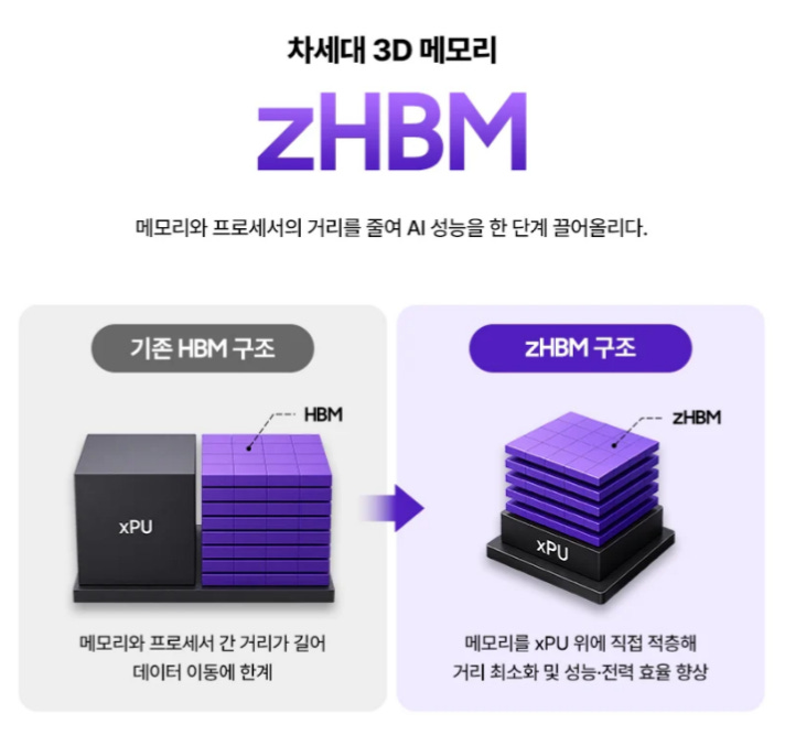
Samsung’s zHBM concept changes the geometry by vertically stacking HBM directly above the AI accelerator.
Samsung 的 zHBM 概念改變了此幾何架構,將 HBM 直接垂直堆疊於 AI 加速器上方。
The purpose is straightforward: reduce the physical distance over which data must travel between memory and logic. Shorter electrical paths can potentially improve bandwidth, reduce energy consumed by data movement, increase package-level density, and reduce communication latency.
其目的非常明確:縮減資料在記憶體與邏輯元件之間傳輸的物理距離。較短的電氣路徑有望提升頻寬、降低資料移動所需的能耗、增加封裝層級的密度,並減少通訊延遲。
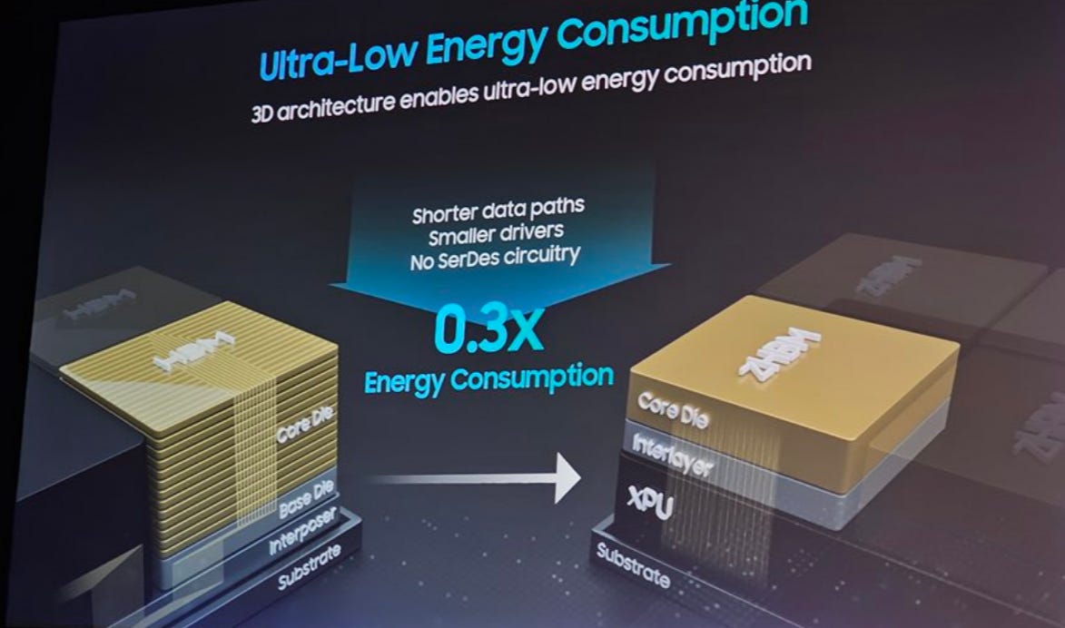
Samsung says a next-generation interface incorporating zHBM could provide approximately eight times the performance of HBM5. With next-generation wafer-bonding technology, the company projects more than ten times the memory density, three times the energy efficiency, and a reduction in thermal resistance of more than half compared with HBM5. These remain architectural targets rather than verified commercial-product specifications, but they indicate the direction Samsung wants the industry to consider.
三星表示,整合 zHBM 的次世代介面可提供約 HBM5 八倍的效能。透過次世代晶圓鍵結技術,該公司預估與 HBM5 相比,記憶體密度將提升十倍以上、能源效率提高三倍,且熱阻降低超過一半。這些目前仍屬架構目標,而非經驗證的商用產品規格,但已指明三星希望產業界考量的發展方向。
Another strategically important feature is the proposed interlayer between the memory and accelerator. Samsung says customer-specific intellectual property could be incorporated into this layer to expand memory capacity or improve accelerator performance.
另一項具戰略重要性的特色,是 proposed 於記憶體與加速器之間的層間結構。三星表示,可將客戶專屬的智慧財產權整合至此層,以擴充記憶體容量或提升加速器效能。
That suggests zHBM is not simply a vertically repositioned memory stack. It could eventually become a configurable integration platform combining memory, interface logic, power-management functions, and customer-specific circuitry.
這意味著 zHBM 不僅僅是垂直重新定位的記憶體堆疊。它最終可能發展成為一個可配置的整合平台,結合記憶體、介面邏輯、電源管理功能以及客戶專屬電路。
In other words, Samsung is trying to turn the boundary between HBM and the accelerator into another area of architectural differentiation.
換言之,三星正試圖將 HBM 與加速器w之間的邊界,轉化為另一個架構差異化的關鍵領域。
Samsung’s Financial Results Already Pointed in This Direction
三星的財務業績早已指向這一方向
The FMS presentation should not be viewed as an isolated exhibition concept.
不應將此次 FMS 發表會視為單一的展示概念。
In its second-quarter 2026 results, Samsung said its foundry performance was supported by demand for HBM base dies and strong orders from U.S. customers. The company also reported expanding engagements for 2-nanometer high-performance computing designs and said it planned to increase sales of 4-nanometer base-die products during the second half of 2026.
在 2026 年第二季財報中,三星表示其晶圓代工表現受惠於 HBM 基礎晶片的需求以及來自美國客戶的強勁訂單。該公司亦報告指出,2 奈米高效能運算設計案的參與持續擴大,並計劃於 2026 年下半年提升 4 奈米基礎晶片產品的銷售量。
These developments show that the integration of memory and logic is already influencing foundry orders and process-roadmap decisions.
這些發展顯示,記憶體與邏輯的整合已開始影響晶圓代工訂單製程路線圖的決策。
An HBM base die is no longer merely a passive supporting component. As interfaces become more complex and customers pursue customized HBM architectures, the base die increasingly incorporates advanced control, communication, and power-management functions. This creates a stronger connection between memory suppliers, logic foundries, accelerator designers, and packaging providers.
HBM 基底晶圓已不再只是被動的支撐元件。隨著介面日益複雜,且客戶追求客製化的 HBM 架構,基底晶圓越來越多地整合了先進的控制、通訊與電源管理功能。這使得記憶體供應商、邏輯晶圓代工廠、加速器設計業者以及封裝服務商之間的連結更加緊密。
Samsung therefore has a strategic reason to connect its memory, foundry, and advanced-packaging businesses under one narrative.
因此,三星有戰略上的理由將其記憶體、晶圓代工與先進封裝業務整合於同一敘事之下。
Its objective is to position itself not simply as a DRAM supplier or an alternative advanced-node foundry, but as one of the few integrated manufacturers capable of offering memory, logic manufacturing, bonding, packaging, and system optimization within a common development environment.
其目標是將自身定位為不僅僅是 DRAM 供應商或替代性先進製程晶圓代工廠,而是少數能夠在共同開發環境中提供記憶體、邏輯製造、鍵結、封裝及系統優化的整合型製造商之一。
Supply Chain Impact: Packaging Becomes a Product-Definition Layer
供應鏈影響:封裝成為產品定義層
The first major supply-chain implication is that advanced packaging will continue to gain strategic importance.
先進封裝將持續提升其戰略重要性,這是供應鏈面臨的首要重大影響。
Platforms such as CoWoS, SoIC, InFO, EMIB, and Foveros have already become central to AI accelerator production. However, in a conventional 2.5D package, memory and logic remain separate components placed laterally on an interposer or redistribution platform.
諸如 CoWoS、SoIC、InFO、EMIB 和 Foveros 等平台,已成為 AI 加速器生產的核心。然而,在傳統的 2.5D 封裝中,記憶體與邏輯仍為獨立元件,橫向放置於中介層或重分佈平台上。
A vertically integrated memory-logic architecture changes the role of packaging.
垂直整合的記憶體 - 邏輯架構將改變封裝的角色。
Packaging would no longer function mainly as the process that connects completed dies. It would help determine the achievable bandwidth, power efficiency, thermal profile, memory capacity, and physical density of the final computing module.
封裝將不再僅是連接已完成晶粒的製程,更將決定最終運算模組所能達到的頻寬、電源效率、熱特性、記憶體容量與實體密度。
This raises the strategic value of several capabilities:
這提升了以下幾項能力的戰略價值:
Hybrid bonding and ultra-fine-pitch interconnects
混合鍵結與超細間距互連技術
Wafer-to-wafer and die-to-wafer integration
晶圓對晶圓及晶粒對晶圓整合
Temporary bonding, wafer thinning, and debonding materials
臨時鍵結、晶圓減薄與解鍵結材料
Bonding-surface preparation and contamination control
接合表面製程與污染控制
Wafer-level inspection and overlay metrology
晶圓級檢測與套刻量測
Known-good-die screening and pre-bond testing
已知良品晶粒篩選與接合前測試
Thermal-interface materials and heat-spreading structures
熱介面材料與散熱結構
Warpage-control films, underfills, and low-stress dielectric materials
翹曲控制薄膜、底部填充膠及低應力介電材料
The commercial opportunity is not limited to traditional outsourced semiconductor assembly and test providers. Foundries, memory manufacturers, equipment suppliers, specialty-material companies, substrate producers, and thermal-solution vendors will all be pushed into earlier stages of product development.
商業機會不僅限於傳統的半導體封裝測試代工廠。晶圓代工廠、記憶體製造商、設備供應商、特殊材料公司、基板生產商以及散熱解決方案供應商,都將被推向產品開發的更早期階段。
Yield and Testing May Become the Most Difficult Constraints
良率與測試可能成為最嚴峻的瓶頸
The attraction of 3D integration is clear, but its manufacturing economics are unforgiving.
3D 整合的吸引力顯而易見,但其製造經濟性卻極為嚴苛。
When several expensive dies are bonded into one structure, the effective yield depends on every component and every bonding interface functioning correctly. A defect in the accelerator, memory stack, interlayer, or bonding process can reduce the value of the complete module.
當多個昂貴的晶粒鍵結成單一結構時,整體良率取決於每個元件與每個鍵結介面是否皆能正常運作。加速器、記憶體堆疊、層間介質或鍵結製程中任何一處出現缺陷,都可能降低完整模組的價值。
This makes known-good-die strategies, wafer-level testing, high-speed interface validation, thermal-stress testing, and non-destructive inspection increasingly important.
這使得已知合格晶粒(Known-Good-Die)策略、晶圓級測試、高速介面驗證、熱應力測試以及非破壞性檢測變得日益重要。
Testing must also occur earlier.
測試也必須更早進行。
In conventional packaging, some failures can be identified after assembly. In tightly integrated 3D architectures, waiting until final system testing may be too expensive. Suppliers will need more comprehensive electrical and structural inspection before bonding, during stacking, and after package completion.
在傳統封裝中,部分缺陷可在組裝後被識別。然而,在高度整合的 3D 架構中,若等到最終系統測試才進行檢測,成本可能過於高昂。供應商必須在接合前、堆疊過程中以及封裝完成後,實施更全面的電性與結構檢驗。
Probe-card companies, burn-in system suppliers, optical and X-ray inspection vendors, metrology companies, and test-equipment manufacturers could therefore become important beneficiaries of deeper memory-logic integration.
因此,探針卡廠商、老化測試系統供應商、光學與 X 射線檢測設備供應商、量測公司以及測試設備製造商,都可能成為記憶體與邏輯更深層整合的重要受益者。
At the same time, repairability will become more complicated. A laterally positioned HBM stack may be difficult to replace, but a vertically bonded memory structure could be even less serviceable. This creates a trade-off among performance, yield, cost, and module recoverability that must be resolved before zHBM-like designs can enter high-volume production.
與此同時,可維修性將變得更為複雜。側向放置的 HBM 堆疊可能難以更換,但垂直鍵結的記憶體結構甚至更難維護。這在效能、良率、成本與模組可恢復性之間產生了權衡,必須在 zHBM 類似設計進入大量生產之前解決。
Thermal Management Must Be Designed From the Beginning
熱管理必須從一開始就納入設計
Samsung highlights lower thermal resistance as one of zHBM’s expected advantages. However, vertical integration does not automatically solve the thermal problem.
三星強調較低的熱阻是 zHBM 的預期優勢之一。然而,垂直整合並不會自動解決散熱問題。
Placing memory above a high-power accelerator creates a highly concentrated heat source. The accelerator may generate substantially more heat than the memory, while HBM performance and reliability remain sensitive to temperature.
將記憶體置於高功率加速器上方會形成高度集中的熱源。加速器產生的熱量可能遠高於記憶體,而 HBM 的效能與可靠性仍對溫度極為敏感。
The design must therefore establish an effective thermal path without damaging signal integrity, increasing mechanical stress, or creating excessive package height.
因此,該設計必須建立有效的散熱路徑,同時不得損害訊號完整性、增加機械應力或導致封裝高度過大。
This will require early collaboration across chip architects, packaging engineers, cooling-system suppliers, and materials companies. Thermal-interface materials, heat spreaders, lid structures, backside power-delivery concepts, cold plates, and potentially direct-liquid-cooling designs will have to be considered as parts of the semiconductor architecture—not as solutions added after the chip has been completed.
這需要晶片架構師、封裝工程師、冷卻系統供應商與材料廠商進行早期協作。熱介面材料、散熱片、蓋體結構、背面供電概念、冷板,以及潛在的直接液冷設計,都必須被視為半導體架構的一部分,而非在晶片完成後才追加的解決方案。
The implication for the supply chain is important: thermal management will move closer to the semiconductor design cycle and could become a source of customer-specific differentiation.
這對供應鏈的意義重大:熱管理將更緊密地融入半導體設計週期,並可能成為客戶專屬差異化的關鍵來源。
zNAND-O and V10 BV-NAND Expand the 3D Strategy Beyond HBM
zNAND-O 與 V10 BV-NAND 將 3D 策略擴展至 HBM 之外
Samsung’s FMS strategy was not limited to DRAM.
三星於 FMS 的策略並不侷限於 DRAM。
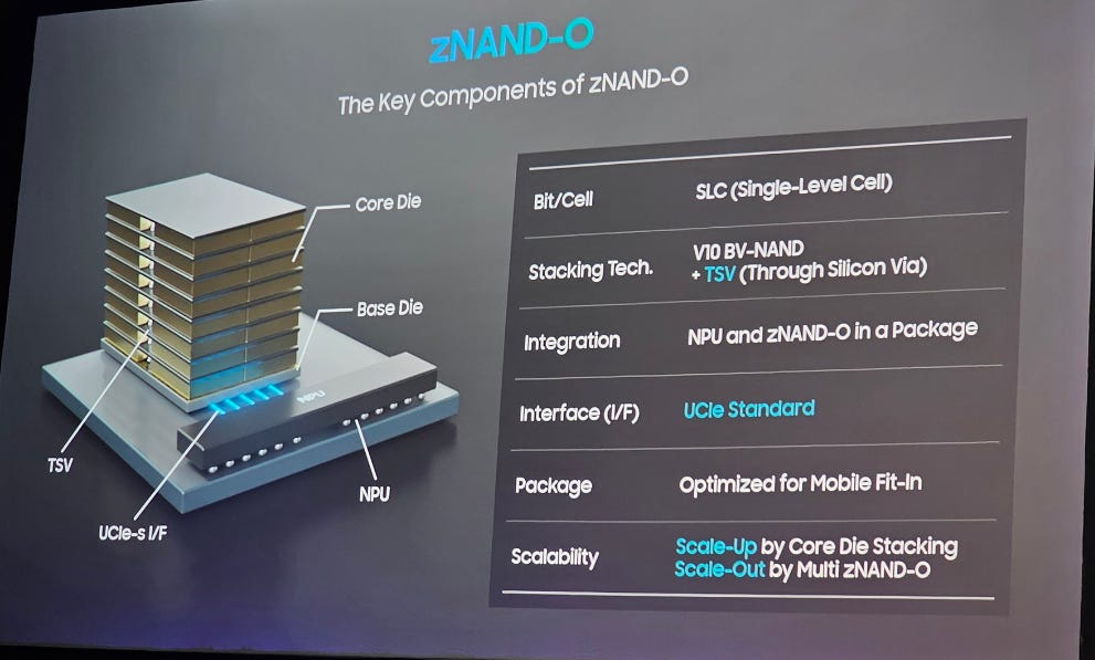
The company also introduced zNAND-O, a high-performance NAND concept being developed in four- and eight-layer configurations. Samsung is targeting edge-AI applications that require higher I/O performance, low latency, and efficient use of physical space.
該公司亦推出了 zNAND-O,這是一款正在開發四層與八層組態的高效能 NAND 概念產品。三星鎖定需要更高 I/O 效能、低延遲以及高效利用實體空間的邊緣 AI 應用。
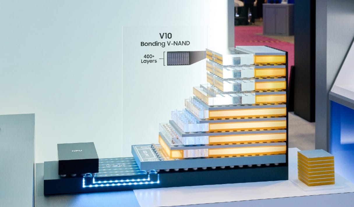
Its V10 BV-NAND uses wafer bonding to separate and optimize the memory-cell and peripheral-logic structures before combining them. The architecture contains more than 400 layers and is designed to increase storage density while improving read, write, and I/O performance. Samsung says the bonding architecture raises memory density by approximately 58% compared with V9.
其 V10 BV-NAND 採用晶圓接合技術,將記憶體單元與周邊邏輯結構分離並進行最佳化,隨後再予以整合。此架構包含超過 400 層,旨在提升儲存密度,同時改善讀取、寫入及 I/O 效能。三星表示,相較於 V9,此接合架構可將記憶體密度提升約 58%。

The important message is that wafer bonding is moving from a specialized packaging technique into a broader memory-manufacturing strategy.
關鍵訊息在於,晶圓接合技術正從一項專門的封裝製程,轉變為更廣泛的記憶體製造策略。
For NAND manufacturers, separately optimizing the cell array and peripheral circuitry can provide greater design flexibility than building both structures through a single sequential process. But it also increases demand for precise bonding equipment, wafer alignment, surface treatment, defect inspection, thin-wafer handling, and bonding-interface control.
對 NAND 製造商而言,分別優化記憶胞陣列與周邊電路,相較於透過單一順序製程建構這兩種結構,能提供更大的設計彈性。然而,這也提高了對精密接合設備、晶圓對準、表面處理、缺陷檢測、薄晶圓搬運以及接合介面控制的 demand。
FMS 2026 therefore points to a convergence between front-end memory fabrication and advanced back-end integration.
因此,FMS 2026 標誌著前端記憶體製造與後端先進整合的匯流。


ASML’s Expansion Confirms That Pressure Will Continue Upstream
ASML 的擴張證實上游壓力將持續
The transition toward more complex memory and logic integration will not reduce demand for front-end equipment.
朝向更複雜的記憶體與邏輯整合之轉型,並不會降低對前段製程設備的需求。
On July 15, ASML raised its 2026 revenue outlook and said AI-related investment was continuing to drive demand for advanced logic and memory. The company plans to increase its 2027 low-NA EUV capacity by 30% from its 2026 level of approximately 65 systems. It also plans a 30% increase in DUV immersion capacity from a 2026 base of approximately 130 systems.
7 月 15 日,ASML 上調其 2026 年營收展望,並表示人工智慧(AI)相關投資持續推動先進邏輯與記憶體的需求。該公司計畫將其 2027 年低數值孔徑(low-NA)極紫外光(EUV)產能,較 2026 年約 65 台系統的基準提升 30%。同時,也計畫將深紫外光(DUV)浸潤式微影產能,較 2026 年約 130 台系統的基準提升 30%。
This is relevant because more advanced packaging does not replace wafer-fabrication intensity. Customized HBM base dies, advanced logic nodes, peripheral NAND circuitry, interface dies, and specialized interlayers all require additional lithography, deposition, etching, cleaning, metrology, and inspection.
此點至關重要,因為更先進的封裝技術並未取代晶圓製造的密集度。客製化的高頻寬記憶體(HBM)基底晶片、先進邏輯製程節點、周邊 NAND 電路、介面晶片以及專用中介層,皆需要額外的微影、沉積、蝕刻、清洗、量測與檢測製程。
The industry is therefore facing simultaneous pressure at both ends of the manufacturing chain: more complex front-end processing and more demanding back-end integration.
因此,半導體產業正面臨製造鏈兩端的雙重壓力:前段製程更為複雜,後段整合的要求也更为嚴苛。
That combination suggests that equipment, materials, packaging, testing, and thermal capacity will remain structurally tight even if individual memory-product shortages begin to ease.
此組合意味著,即使個別記憶體產品的缺貨狀況開始緩解,設備、材料、封裝、測試及散熱產能仍將持續面臨結構性緊缺。

7月16日7 月 16 日
China Adds a Long-Term Capacity and Geopolitical Variable
中國增添長期產能與地緣政治變數
The memory cycle is also being reshaped by China’s expansion.
記憶體週期也正因中國的擴張而重塑。
Reuters reported on August 3 that CXMT was considering a second 12-inch DRAM facility in Beijing’s Yizhuang district. Existing and planned projects in Beijing, Hefei, and Shanghai could eventually more than double the company’s production capacity to over 600,000 wafers per month, although the new Beijing project remains at an early stage and its final capacity and investment have not been determined.
路透社 8 月 3 日報導,長鑫儲存(CXMT)正考慮在北京亦莊區興建第二座 12 吋 DRAM 廠。北京、合肥與上海現有及規劃中的專案,最終可能將該公司的產能提升一倍以上,達到每月超過 60 萬片晶圓;不過,新的北京專案仍處於早期階段,其最終產能與投資金額尚未確定。
This means the memory market can no longer be assessed only through near-term HBM shortages and pricing.
這意味著記憶體市場已無法僅透過近期的 HBM 短缺與價格走勢來評估。
The industry must simultaneously consider Chinese capacity expansion, equipment restrictions, domestic substitution, government financing, technology gaps, and the possibility of longer-term supply pressure in conventional DRAM segments.
產業必須同時考量中國的產能擴張、設備限制、國產替代、政府融資、技術落差,以及傳統 DRAM 區塊可能面臨的長期供應壓力。
Leading suppliers may increasingly respond by moving toward differentiated products that are difficult to compete with through capacity alone. Customized HBM, advanced base dies, processing-in-memory, wafer-bonded NAND, and memory-logic integration all fit this strategy.
領先供應商可能愈來愈傾向採取差異化產品策略,使競爭對手難以單靠產能與之抗衡。客製化 HBM、先進基底晶片(base dies)、存內運算(processing-in-memory)、晶圓接合式 NAND,以及記憶體與邏輯整合,皆符合此策略方向。

7月28日7 月 28 日
The Competitive Battle Is Shifting to System Assembly
競爭戰場正轉向系統組裝
The broader conclusion from Samsung’s FMS presentation is that the value center of AI semiconductors may be shifting from the individual compute die toward the ability to assemble and optimize the complete computing system.
三星於 FMS 研討會發表內容所導出的更廣泛結論是:AI 半導體的價值中心,可能正從單一運算晶粒,轉向組裝與優化完整運算系統的能力。
If two accelerators using similar logic technology deliver substantially different performance because of their memory placement, bonding structure, thermal architecture, and package-level bandwidth, then process-node leadership alone will not determine the winner.
若兩款採用相似邏輯技術的加速器,因記憶體配置、接合結構、散熱架構及封裝層級頻寬等因素而呈現顯著不同的效能表現,則僅憑製程節點的領先已不足以決定勝者。
The leading platform will be the one that can jointly optimize:
領先的平台將是能夠共同優化以下項目的平台:
Accelerator architecture加速器架構
HBM and customized base dies
HBM 與客製化基底晶粒
Interconnect and bonding technology
互連與接合技術
Advanced packaging先進封裝
Package substrate and power delivery
封裝基板與電源傳輸
Thermal management熱管理
Testing and manufacturing yield
測試與製造良率
Cloud-customer deployment requirements
雲端客戶的部署需求
This is why Samsung’s strategy matters to TSMC, Intel, SK hynix, Micron, OSAT companies, and the broader packaging ecosystem.
這正是三星的策略對台積電、英特爾、SK 海力士、美光、OSAT 廠商以及更廣泛的封裝生態系至關重要的原因。
TSMC retains a powerful position through its advanced-node manufacturing and established packaging platforms. Samsung, however, is presenting a different competitive model: a vertically integrated IDM combining memory, foundry, and packaging under one development structure.
台積電憑藉其先進製程製造與既有的封裝平台,仍保有強大的市場地位。然而,三星則提出了一種不同的競爭模式:一種垂直整合的 IDM 架構,將記憶體、晶圓代工與封裝技術納入單一的開發體系之下。
The next competition may therefore be less about which company possesses the best individual component and more about which ecosystem can coordinate the greatest number of critical technologies within the shortest development cycle.
因此,下一階段的競爭焦點可能不再取決於哪家企業擁有最佳的單一元件,而在於哪個生態系能夠在最短的開發週期內,有效協調最關鍵的多項技術。
SemiVision ViewSemiVision 視角
zHBM remains a concept architecture. Samsung has not yet disclosed a commercial production schedule, customer qualification program, manufacturing yield, cost structure, or confirmed deployment roadmap.
zHBM 仍屬概念架構。三星尚未揭露量產時程、客戶認證計畫、製程良率、成本結構或已確認的部署路線圖。
Major challenges remain, including thermal concentration, bonding yield, test accessibility, repairability, package cost, design standardization, and customer adoption.
重大挑戰依然存在,包括熱集中、接合良率、測試可及性、可修復性、封裝成本、設計標準化以及客戶採用度。
Samsung has introduced a direction—not yet secured a market.
三星已提出發展方向,但尚未確立市場地位。
Nevertheless, the direction deserves close attention because it appears at the intersection of several structural trends. SIA projects that worldwide semiconductor sales could reach $1.5 trillion in 2026, driven by AI, advanced computing, communications, healthcare, and defense. Since 2020, more than $770 billion of private semiconductor investment has also been announced in the United States, showing that market expansion and supply-chain restructuring are occurring at the same time.
然而,此發展方向值得密切關注,因為它出現在多項結構性趨勢的交匯點。美國半導體產業協會(SIA)預估,受人工智慧、先進運算、通訊、醫療保健與國防等領域驅動,2026 年全球半導體銷售額有望達到 1.5 兆美元。自 2020 年以來,美國亦宣布超過 7,700 億美元的民間半導體投資,顯示市場擴張與供應鏈重組正同步進行。
Over the next two years, the most important question may not be whether HBM adds more layers. It will be whether AI accelerators begin moving from side-by-side GPU-and-HBM packages toward deeper 3D memory-logic integration.
在未來兩年,最重要的問題或許不在於 HBM 是否增加更多層數,而在於 AI 加速器是否將從 GPU 與 HBM 並列封裝的模式,轉向更深度的 3D 記憶體 - 邏輯整合架構。
Four indicators deserve particular attention:
有四項指標特別值得關注:
First, whether Samsung discloses zHBM customer collaborations, engineering samples, qualification schedules, or production targets.
首先,三星是否會公開 zHBM 的客戶合作、工程樣品、認證時程或生產目標。
Second, whether TSMC, Intel, SK hynix, Micron, Nvidia, or major custom-accelerator developers reveal comparable memory-on-logic architectures.
其次,台積電(TSMC)、英特爾(Intel)、SK 海力士(SK hynix)、美光(Micron)、輝達(Nvidia)或主要自訂加速器開發商,是否會揭露類似的記憶體置於邏輯晶片之上(memory-on-logic)架構。
Third, whether hybrid-bonding equipment, wafer-bonding materials, advanced test systems, thermal solutions, and high-end packaging suppliers announce new capacity or long-term agreements.
第三,混合鍵合設備、晶圓鍵合材料、先進測試系統、散熱解決方案及高階封裝供應商,是否會宣布新增產能或長期合約。
Fourth, whether cloud service providers begin prioritizing module-level bandwidth density and energy efficiency over isolated accelerator specifications.
第四,雲端服務供應商是否開始優先考量模組層級的頻寬密度與能源效率,而非單獨的加速器規格。
If these signals emerge, FMS 2026 will not be remembered simply as the event where Samsung introduced another memory concept.
若這些訊號成真,FMS 2026 將不會僅被視為三星推出另一項記憶體概念的盛會。
It could mark the beginning of a broader revaluation of the AI semiconductor supply chain—one in which memory, logic, packaging, thermal design, and manufacturing yield become inseparable parts of the same competitive architecture.
這可能標誌著人工智慧半導體供應鏈更廣泛重估的開端——在這樣的架構中,記憶體、邏輯運算、封裝技術、散熱設計與製程良率,將成為同一競爭體系中密不可分的組成要素。
Thanks for reading SEMIVISION @_@! This post is public so feel free to share it.
感謝閱讀 SEMIVISION @_@!本文為公開文章,歡迎自由分享。


Share分享
Previous上一頁