The Next AI Packaging Bottleneck: Why TSMC Is Preparing for Glass and CoPoS
The Next AI Packaging Bottleneck: Why TSMC Is Preparing for Glass and CoPoS
- Source: SemiVision
- Author: SEMIVISION
- Published: 2026-07-30T09:44:23+08:00
- URL: https://tspasemiconductor.substack.com/p/the-next-ai-packaging-bottleneck (1) The Next AI Packaging Bottleneck: Why TSMC Is Preparing for Glass and CoPoS


The Next AI Packaging Bottleneck: Why TSMC Is Preparing for Glass and CoPoS
Original Article By SemiVision Research [Reading time: 15 mins]

Jul 30, 2026
∙ Paid
The Next AI Packaging Bottleneck: Why TSMC Is Preparing for Glass and CoPoS
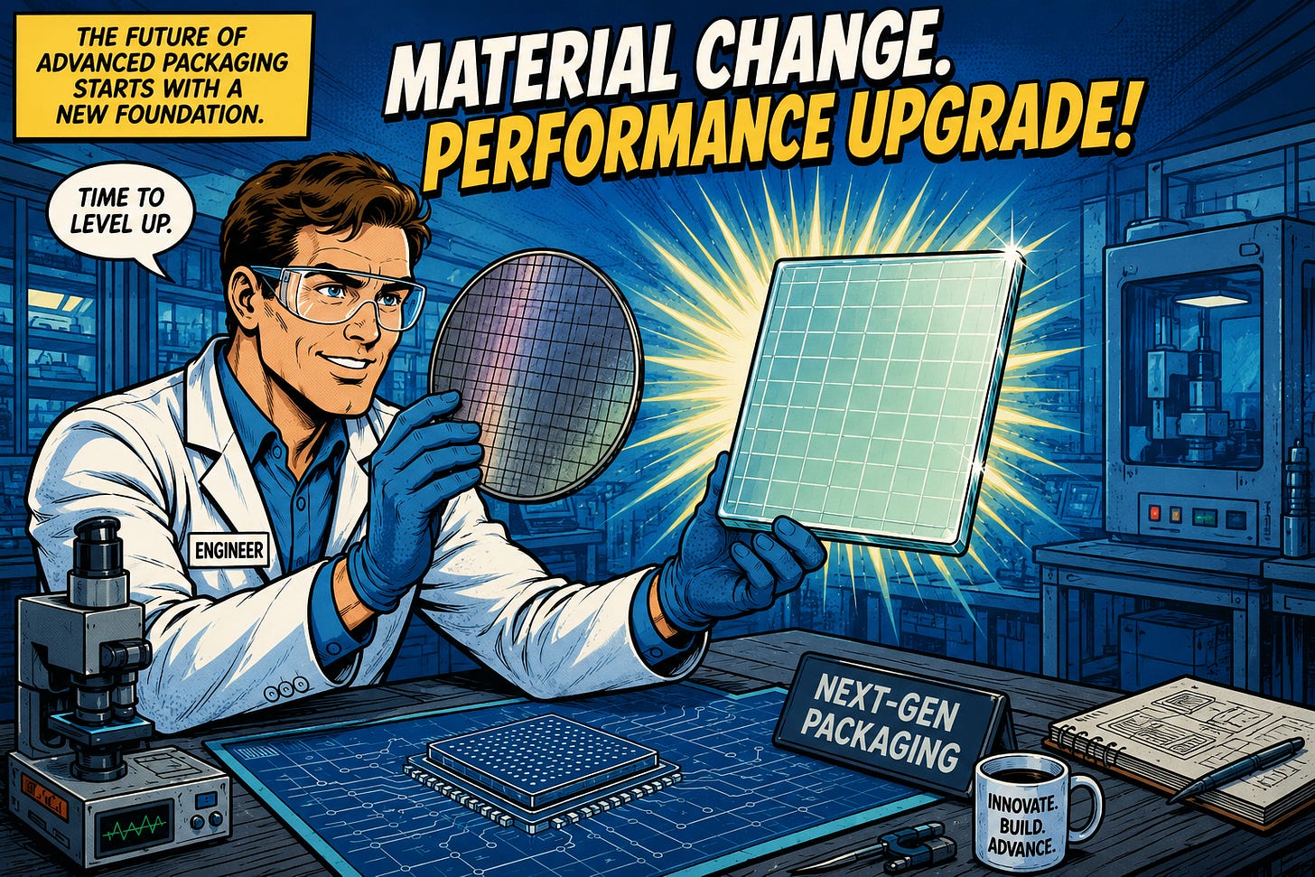
Glass is rapidly becoming one of the most discussed materials in advanced semiconductor packaging. Yet much of the market narrative remains oversimplified.
SemiVision found that some investors assume that TSMC’s CoPoS roadmap means the company is preparing to replace silicon interposers with glass. Others believe glass core substrates will immediately displace ABF substrates once panel-level packaging enters production. Neither interpretation fully reflects how TSMC is likely approaching the technology.
TSMC’s strategy is more gradual and more pragmatic.
The company is not making a single, all-in transition from silicon and organic materials to glass. Instead, it is building a multi-stage packaging roadmap in which different forms of glass solve different engineering problems at different times.
The first step is not necessarily a glass interposer. It is panelization.
CoPoS, or Chip-on-Panel-on-Substrate, moves advanced packaging from a circular wafer format toward a rectangular panel architecture. Glass initially serves primarily as a temporary carrier that enables large-area redistribution-layer processing. At a later stage, glass may move deeper into the package as a structural substrate. Only after the manufacturing ecosystem matures could glass become a practical interposer platform for the largest AI systems.
This distinction is critical.
CoPoS addresses the limits of wafer-based manufacturing. Glass core substrates address the mechanical and dimensional limits of organic substrates. Glass interposers address the electrical and routing limits of existing interposer architectures.
These are related technologies, but they are not the same technology.
AI Is Turning Packaging into a System-Level Bottleneck
The rapid expansion of artificial intelligence infrastructure is changing the physical dimensions of semiconductor packages.
AI accelerators are becoming larger. The number of HBM stacks surrounding each compute die is increasing. Chiplet architectures are adding more logic, memory, I/O and power-management components inside a single package. Meanwhile, the electrical distance between these components must remain extremely short to preserve bandwidth and energy efficiency.
As a result, advanced packaging is no longer simply a back-end manufacturing process. It has become a system-level platform responsible for signal integrity, power delivery, thermal management and mechanical stability.
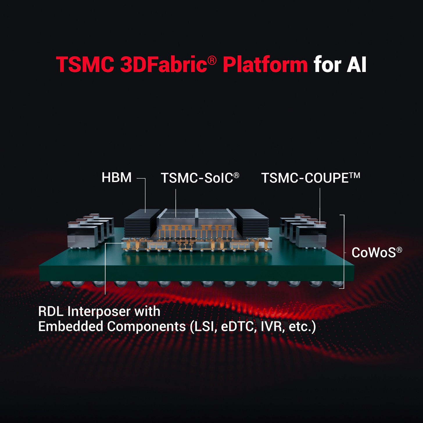
Source: TSMC
TSMC’s CoWoS platform has been central to this transformation.
CoWoS uses a wafer-based process to integrate GPUs, ASICs and HBM through silicon interposers or redistribution-layer structures. The platform is mature, highly integrated and supported by a broad manufacturing ecosystem. However, it is still constrained by the geometry of a circular wafer.
As AI packages become larger, fewer packages can be placed on each 300-millimeter wafer. The unused area around the edge increases, while each package consumes a larger share of the wafer. Adding more CoWoS capacity can alleviate shortages, but it cannot eliminate the fundamental geometric limitation.
This is why the next packaging transition is increasingly described as a move “from round to square.”
A rectangular panel can provide significantly higher area utilization than a circular wafer. It can also support larger package dimensions and potentially improve manufacturing economics once yields and process control become sufficiently mature.
CoPoS is TSMC’s response to this scaling problem.
Below we will share:
CoPoS Is Primarily a Panelization Strategy
Glass Carrier, Glass Core and Glass Interposer Must Be Separated
Glass core Substrate Timeline
Intel Is Pursuing a Different Glass Strategy
Horizontal and Vertical Scaling Will Develop Together
Related report: SemiVision Technical insight Report – Glass, Advanced Package and TGV – Section 1
For more details and inquires please contact:jett@semivisiontw.com
CoPoS Is Primarily a Panelization Strategy
The most important point is that CoPoS should not automatically be interpreted as a glass-substrate platform.
In its initial form, CoPoS is expected to use a large rectangular glass carrier during panel-level redistribution-layer processing. The glass carrier provides the flatness and dimensional stability required to handle a large panel through lithography, deposition, plating and assembly processes.
Once the redistribution layers are completed, the package structure can be transferred to an organic substrate.
In other words, glass may initially function as a manufacturing carrier rather than the permanent electrical or mechanical foundation of the final package.
This approach allows TSMC to address the most immediate bottleneck—the limited usable area of a circular wafer—without simultaneously introducing all the risks associated with glass core substrates or glass interposers.
It also reflects a broader pattern in TSMC’s technology strategy. The company generally avoids changing too many critical process variables at the same time. Instead, it introduces new materials and manufacturing architectures in controlled stages, allowing customers, equipment suppliers and material vendors to accumulate production experience before the technology becomes structurally indispensable.
CoPoS therefore represents a manufacturing architecture transition before it becomes a complete material-platform transition.
CoPoS Is More Than a Larger Version of CoWoS
It would also be misleading to describe CoPoS as simply “CoWoS on a rectangular panel.”
The longer-term significance of CoPoS lies in its potential to turn panel-level redistribution layers into a multifunctional system platform.
Future panel-level packages may integrate local silicon interconnects, embedded deep-trench capacitors, integrated voltage regulators and more sophisticated power-delivery structures. These components could allow the package to manage not only data transmission but also power integrity and voltage regulation across increasingly large AI systems.
This matters because power delivery is becoming one of the defining constraints of AI accelerator design.
A next-generation AI package may contain multiple compute dies, numerous HBM stacks, high-speed I/O chiplets and optical-interface components. Delivering stable power across such a large physical area becomes increasingly difficult. Resistance, inductance, thermal gradients and voltage droop all become more severe as package dimensions increase.
The packaging platform must therefore evolve from a passive interconnection layer into an active system-enablement platform.
From this perspective, CoPoS is not only about manufacturing more packages per panel. It is about creating enough physical area and architectural flexibility to integrate the next generation of electrical, thermal and power-management functions.
Glass Carrier, Glass Core and Glass Interposer Must Be Separated
The word “glass” is often used too loosely in discussions about advanced packaging. Three different applications need to be distinguished.

Glass Carrier
A glass carrier is primarily a temporary manufacturing platform.
Its role is to support large-area redistribution-layer processing while maintaining flatness, rigidity and dimensional accuracy. After the required layers are formed, the structure may be debonded and transferred to another substrate.
This is the most immediate role of glass in the early CoPoS roadmap.
Glass Core Substrate
A glass core substrate is a permanent structural component that could eventually replace the organic core used in conventional ABF substrates.
Its main advantages are mechanical and dimensional.
As AI packages move toward dimensions exceeding 100 millimeters on each side, organic substrates face increasing difficulties with warpage, coefficient-of-thermal-expansion mismatch and dimensional stability. The number of build-up layers may also rise, increasing process complexity and yield risk.
Glass offers a lower coefficient of thermal expansion, higher flatness and better dimensional stability than conventional organic materials. These characteristics make it attractive for very large packages in which mechanical deformation can damage solder joints, disrupt fine-pitch interconnections or reduce assembly yield.
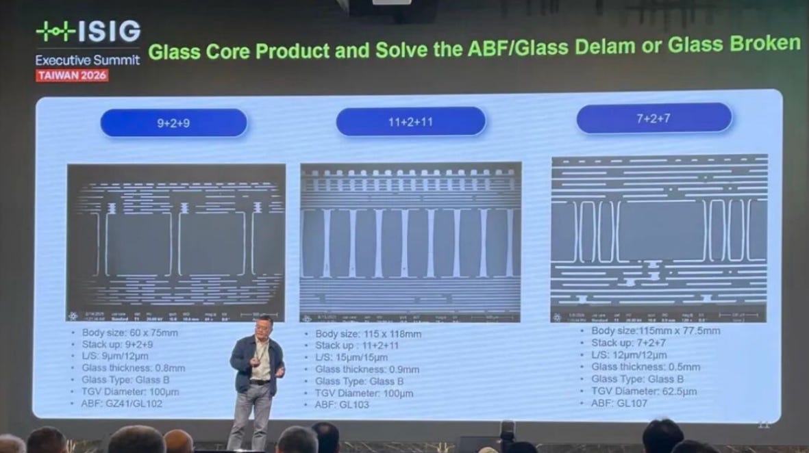
Glass core substrates therefore address the area-scaling limits of ABF substrates.
Glass substrate commercialization is approaching, with leading industry players accelerating the development of the entire supply chain.
The development of the glass substrate industry from 2026 to 2030 can be divided into four key stages. Overall capacity expansion is expected to follow an S-curve growth pattern, gradually transforming glass substrates from an emerging technological breakthrough into a mainstream commercial material.
2026: Technology Validation and Initial Adoption
The industry is expected to remain at the bottom of the S-curve, focusing on technical validation, customer qualification, and early-stage adoption. This stage will represent the critical transition from zero to one.
2027: Transition to Scaled Production
The industry may begin moving beyond the validation stage and enter small-volume production. Supply chains, manufacturing processes, and customer applications are expected to become more established.
2028: Accelerated Industry Ramp-Up
Large-scale production is expected to begin across the industry, while improvements in yield and manufacturing efficiency may create a clear cost inflection point. Commercial adoption is likely to accelerate significantly.
2029–2030: Maturity and Volume Expansion
The industry may enter a mature growth phase, supported by greater standardization, a more balanced supply-demand structure, and broad-based commercial deployment. Glass substrates are expected to complete their transition from an emerging technology to a mainstream material platform.
Glass Interposer
A glass interposer would sit between the compute and memory components and the lower substrate, performing a role similar to a silicon or redistribution-layer interposer.
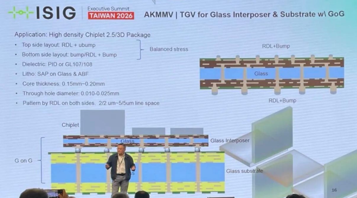
The theoretical advantages are attractive. Glass offers low electrical loss, strong dimensional stability and the potential to support large interposer areas. Through-glass vias can provide vertical connectivity, while multilayer redistribution structures can route high-speed signals across the package.
However, a glass interposer introduces a different class of manufacturing challenges.
These include high-aspect-ratio TGV formation, metallization, copper adhesion, via filling, multilayer alignment, thermal-stress management, microcrack detection and large-area warpage control.
For this reason, glass interposers are likely to remain a longer-term option rather than the immediate foundation of TSMC’s CoPoS strategy.
Why Glass Core May Arrive Before Glass Interposers
The semiconductor industry often assumes that glass interposers will be the most valuable application because they are directly connected to high-bandwidth signal transmission.
However, the most urgent problem in large AI packages may not be interposer density. It may be substrate mechanics.
TSMC has already developed CoWoS-L, which combines redistribution-layer interposers with local silicon interconnects. Instead of using a full-area silicon interposer, CoWoS-L places silicon only where the highest-density connections are needed.

Source: TSMC
This hybrid architecture reduces silicon consumption while preserving high-density connectivity between critical dies. It also benefits from an established process ecosystem, existing production experience and a more mature yield-learning curve.
As a result, TSMC does not need to replace silicon interconnect technology immediately.
The more immediate limitation is the organic substrate beneath the package.
As package area expands, the substrate must maintain flatness across a much larger surface. It must survive repeated thermal cycles while supporting increasingly fine wiring, heavier component loads and more complex power-delivery structures. Organic materials become progressively harder to control under these conditions.
Glass core substrates can address this problem without requiring TSMC to abandon CoWoS-L.
This suggests a more realistic technology sequence:
CoWoS-S
→ CoWoS-L
→ CoPoS with glass carriers and panel-level RDL
→ Glass core substrates
→ Glass interposers
Under this roadmap, glass core technology has a higher near- to medium-term strategic priority than glass interposers.
Glass interposers may eventually become important for extremely large packages after 2030, particularly if silicon interposers become too expensive or too limited in size. But during the next several years, the industry is more likely to focus on panelization, substrate scaling, warpage control and power-delivery integration.
The Real Challenge Is Manufacturing Yield
The advantages of glass are well understood. The production challenges are not.
Glass offers low thermal expansion, excellent flatness, strong high-frequency electrical performance and compatibility with large-area panel processing. Yet these benefits do not automatically translate into high-volume manufacturing.
One major challenge is copper adhesion.
Glass surfaces are smooth and chemically different from organic materials. Building reliable copper interfaces requires surface treatment, adhesion layers and metallization processes that can survive thermal cycling without delamination.
TGV filling presents another challenge.
Through-glass vias must be drilled, metallized and filled without creating voids, cracks or excessive stress. The difficulty increases as via density rises and aspect ratios become more aggressive. Laser drilling, plasma processing, wet chemistry, plating and inspection must all be optimized as one integrated process.
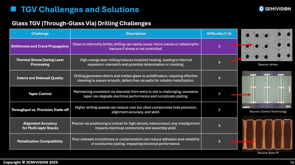
Warpage also remains a central issue.
Although glass itself has strong dimensional stability, a complete package contains multiple materials with different coefficients of thermal expansion. Copper, polymer dielectrics, molding compounds, silicon dies and organic layers respond differently to heat.
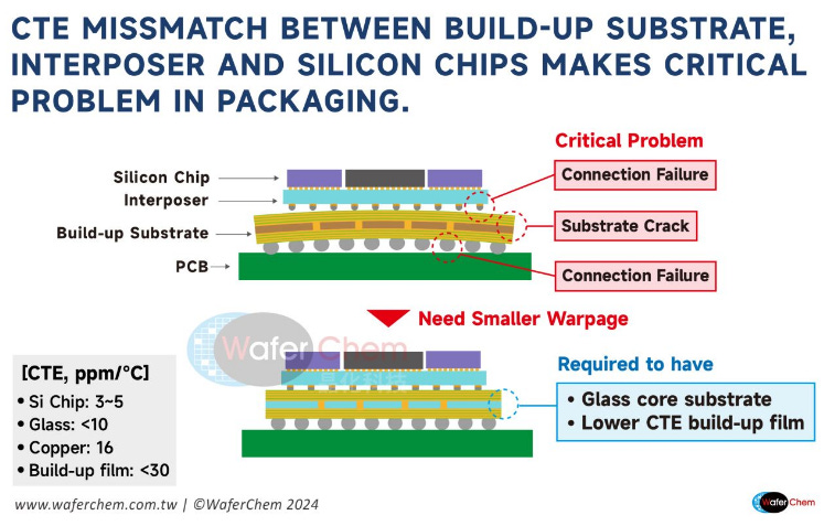
The package can still bend or twist during processing, especially when the layer structure is asymmetrical. Balance films, temporary bonding materials and stress-compensation layers will therefore become critical parts of the material stack.
Inspection is another bottleneck.
Glass is transparent, and internal cracks can be difficult to detect using conventional semiconductor inspection systems. TGV defects, subsurface damage, microcracks and metal-fill problems may require new combinations of optical, acoustic, X-ray and interferometric inspection.
The transition to panel-level manufacturing also forces equipment suppliers to redesign tools originally developed for circular wafers.
Handling systems, chucks, aligners, lithography platforms, deposition chambers, plating tools, laser systems, cleaning systems and metrology equipment must all accommodate larger rectangular formats. Process uniformity across the corners and center of a panel becomes significantly more difficult than across a conventional wafer.
CoPoS therefore represents not only a packaging transition but also an equipment-architecture transition.

7月14日
A New Supply Chain Is Forming Around Panel-Level Packaging
The move from wafers to panels could reshape the division of labor across the semiconductor supply chain.
Traditional semiconductor equipment suppliers remain central because panel-level packaging still requires high-precision lithography, deposition, cleaning, inspection and bonding. However, companies with experience in display-panel processing may gain new relevance.
Display manufacturers understand large glass handling, panel coating, exposure, alignment and defect control. These capabilities are not directly transferable to advanced semiconductor packaging, but they provide a starting point that conventional OSATs and wafer-equipment suppliers may not possess.
This creates potential opportunities for display companies, glass processors, PCB manufacturers and specialized material vendors.

3月20日
The emerging ecosystem can be divided into several critical categories:
Large-area glass carriers and glass-core materials
TGV drilling, metallization and copper-filling equipment
Panel-level lithography and redistribution-layer processing
Temporary bonding and laser-debonding materials
Warpage-control films and stress-balancing materials
Low-loss dielectric and copper-adhesion layers
Panel inspection, metrology and microcrack detection
High-precision handling, cleaning and plasma-treatment systems
The commercial opportunity will not be distributed evenly.
The first beneficiaries are likely to be companies already qualified in TSMC’s CoWoS ecosystem. Advanced packaging requires extensive process integration, and TSMC is unlikely to introduce a completely new supplier base without long validation cycles.
Existing suppliers with experience in wafer cleaning, bonding, temporary carriers, laser processing, plating, inspection and metrology are therefore positioned to extend their capabilities into panel-level platforms.
At the same time, some display and PCB companies could become strategically important if they can meet semiconductor-grade requirements for cleanliness, dimensional control, defect density and traceability.
The key question is not whether a supplier can process glass. It is whether it can process glass at semiconductor yields.
TSMC Is Likely to Maintain Tight Control of the Ecosystem
Advanced packaging has become one of TSMC’s most important competitive advantages.

The company is no longer competing only on transistor density. It is increasingly competing on its ability to combine advanced logic, HBM, chiplets, power delivery and thermal solutions into manufacturable systems.
CoPoS could further strengthen this advantage, but only if TSMC can prevent the technology from becoming a standardized process that competitors can easily reproduce.
This is why supply-chain control will remain strict.
Panel-level packaging requires extensive co-development between TSMC and its equipment and material partners. Suppliers may need to modify tool architectures, chemistries, films and handling systems around TSMC-specific process requirements.
During the early stage, the most valuable suppliers may not be those with the largest production capacity. They may be those willing to dedicate engineering resources, protect process information and accept long qualification cycles.
This creates a high barrier to entry.
It also means that public market discussions about “glass-substrate beneficiaries” may be premature. Many companies can demonstrate glass-processing technology, but only a limited number will achieve the reliability, defect control and integration required for a leading-edge AI package.
The decisive milestone is not a prototype announcement. It is sustained customer qualification and repeat equipment orders.
Intel Is Pursuing a Different Glass Strategy
Intel has been one of the most aggressive proponents of glass core substrates.
Its strategy is closely linked to EMIB, which uses embedded silicon bridges inside a substrate to connect adjacent dies. By combining glass-core substrates with EMIB, Intel aims to support larger packages, finer interconnections and more chiplets within a single system.
This approach differs from TSMC’s initial CoPoS architecture.
Intel is positioning glass as a structural substrate technology, while TSMC is initially using glass to enable panel-level processing before gradually moving it deeper into the package.
Intel may therefore appear more aggressive in glass-core commercialization. However, TSMC retains several strategic advantages.
It controls leading-edge logic manufacturing, advanced packaging integration and a large AI customer base. It also has extensive production experience across CoWoS, SoIC and chiplet integration. These capabilities allow TSMC to introduce glass incrementally without forcing customers to adopt an entirely new package architecture at once.
The competition is therefore not simply a race to launch a glass substrate.
It is a competition to build a complete, high-yield manufacturing ecosystem around extremely large AI packages.
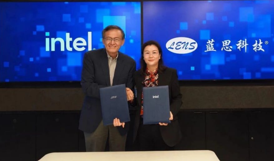
Intel and Lens Technology Collaborate to Enable Advanced Semiconductor Packaging for the AI Era
Horizontal and Vertical Scaling Will Develop Together
TSMC’s future advanced-packaging roadmap is likely to combine two complementary directions.
CoPoS addresses horizontal scaling.
It provides more physical area for GPUs, AI ASICs, HBM stacks, I/O chiplets, power components and potentially co-packaged optics. By moving to panel-level manufacturing, TSMC can support package dimensions that would become increasingly inefficient on circular wafers.
SoIC addresses vertical scaling.
It enables direct die-to-die stacking through hybrid bonding, reducing interconnection distance and improving bandwidth density. Vertical integration can place cache, logic, memory or specialized accelerators directly above or below other dies.
The future AI package may use both approaches simultaneously.
A large CoPoS platform could provide the horizontal foundation, while SoIC stacks multiple functional layers vertically. Glass core substrates could stabilize the larger mechanical structure, while local silicon interconnects and hybrid bonding deliver the highest-density electrical connections.
This would transform advanced packaging into a three-dimensional system architecture rather than a collection of separately packaged chips.
The Next Five Years Will Be About Process Integration, Not Material Hype
Glass has the potential to become a foundational material for next-generation semiconductor packaging. But adoption will be slower and more selective than the current market narrative suggests.
TSMC’s likely strategy can be summarized in three principles.
First, panelization comes before full material replacement.
The immediate objective of CoPoS is to escape the geometric and economic constraints of circular wafer processing. A glass carrier enables this transition without requiring the final package to use a permanent glass substrate.
Second, glass core substrates may be more strategically important than glass interposers during the next stage.
The first major physical limit confronting ultra-large AI packages is likely to be substrate warpage and dimensional stability. Glass core technology directly addresses this problem while allowing TSMC to continue using CoWoS-L and local silicon interconnects.
Third, supply-chain control will matter as much as the material itself.
The winning ecosystem will require integrated progress across glass materials, TGV formation, copper adhesion, dielectric layers, temporary bonding, panel equipment, inspection and warpage management. No single supplier can solve the problem alone.

3月13日
Conclusion: Glass Is a Roadmap, Not a Single Product
TSMC’s view of glass should not be described as a complete commitment or a rejection.
It is better understood as an active but staged strategic deployment.
The company is first using glass to support the transition from wafer-level to panel-level manufacturing. It may then introduce glass core substrates to overcome the mechanical limits of increasingly large ABF structures. Glass interposers could follow later if AI systems eventually require interconnection areas beyond the practical limits of silicon and hybrid RDL architectures.
The central industry signal is clear.
AI packaging is moving beyond the limits of conventional wafers, organic substrates and passive interconnect structures. The next generation of platforms must support larger package areas, more HBM, more chiplets, higher power density and increasingly complex power-delivery networks.
Glass will be part of that transition—but not in the simplistic form the market often assumes.
The most important question is therefore not whether TSMC will adopt glass.
It is where glass will enter the package first, which engineering bottleneck it will solve, and which suppliers can achieve semiconductor-grade yield before the rest of the industry catches up.

2025年4月17日


PreviousNext