CPO’s Biggest Bottleneck Is Not Optics—It Is High-Volume Testing
CPO’s Biggest Bottleneck Is Not Optics—It Is High-Volume Testing
- Source: SemiVision
- Author: SEMIVISION
- Published: 2026-07-27T10:12:02+08:00
- URL: https://tspasemiconductor.substack.com/p/cpos-biggest-bottleneck-is-not-opticsit CPO’s Biggest Bottleneck Is Not Optics—It Is High-Volume Testing


CPO’s Biggest Bottleneck Is Not Optics—It Is High-Volume Testing
Original Article By SemiVision Research [Reading time: 15 mins]

Jul 27, 2026
∙ Paid

Artificial intelligence (AI), high-performance computing (HPC), and hyperscale cloud environments are driving data volumes to unprecedented levels. As GPU clusters and distributed inference engines multiply, the limitations of today’s 224 Gbps infrastructure are clear. The next milestone—448 Gbps per lane—will reshape how data centers are built, cooled, and interconnected.This evolution is about more than speed. It’s about density, power efficiency, and scalability across the entire signal chain.
TE Connectivity (TE) 448G Solutions
CPO’s Biggest Bottleneck Is Not Optics—It Is High-Volume Testing

AI infrastructure is entering a new inflection point.
Over the past few years, the industry’s attention has been concentrated on GPUs, HBM, advanced packaging, CoWoS capacity, data center power delivery, and thermal architecture. However, as AI clusters expand from single-rack systems to multi-rack architectures, and from scale-out networking toward scale-up xPU fabrics, the real constraint on system efficiency is gradually shifting from “compute itself” to “how data moves within the system.”
In other words, the competitive focus of AI systems is moving away from the performance of a single chip and toward high-speed interconnect capability between chips, inside packages, and across racks.
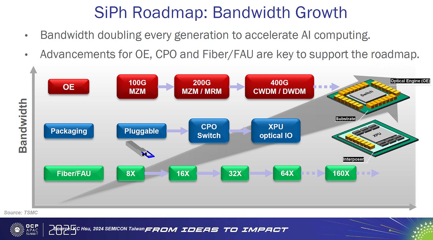
This is why silicon photonics and co-packaged opticsb are moving from research topics into core issues for high-volume manufacturing. In its presentation at the SEMICON Taiwan SiPh Global Summit 2025, Advantest directly pointed out that SiPh/CPO has become a key enabling technology for future AI factories. Today, it is mainly applied in scale-out networking; the next stage will be scale-up xPU fabrics. In other words, optics will no longer be merely part of networking modules. It will move increasingly closer to ASICs, XPUs, and advanced packaging itself.
But this shift also brings anew challenge: once optics enters the package, testing can no longer follow the traditional logic of optical module production lines.Whether CPO can truly achieve mass production will not depend only on whether photonic chips can be designed, nor only on whether packaging can be completed. It will depend on whether the entire industry can establish a repeatable, automated, standardized, and economically viable electro-optical hybrid test system.
2025年7月16日
The Interconnect Bottleneck in AI Systems Is Pushing Optics Inside the Package
The evolution of AI servers is changing the position of the optical communications industry.
In traditional data center architectures, optical modules are mostly located outside the switch or rack, serving the role of long-distance, high-bandwidth data transmission. Optical modules have historically been peripheral I/O components of the system, with relatively clear boundaries separating them from ASICs, GPUs, HBM, and package substrates.
However, the development of AI data centers is breaking down this boundary. As the bandwidth requirements of GPUs, AI ASICs, HBM, and switch chips continue to rise rapidly, the key question is no longer simply whether the chip is fast enough. It is whether data can move in and out of the chip in real time.
The logic behind this shift is clear. Under high-speed, long-distance, and high-density conditions, copper interconnects face multiple challenges, including power consumption, signal integrity, thermal management, and package area constraints. As 800G, 1.6T, and even higher-speed standards become baseline requirements for AI data centers, relying solely on pluggable optical modules or traditional board-level interconnects is becoming increasingly insufficient for next-generation AI fabrics.
Therefore,the value of SiPh and CPO is not merely about converting electrical signals into optical signals. It is about redefining how data moves within computing systems.
In the past, optics mainly solved external system-level transmission problems. In the future, optics will increasingly address internal system interconnect problems. This means the battlefield for optical interconnects will gradually move from outside the rack, switch front panels, and optical module cages toward ASIC packages, interposers, substrates, and even chiplet interfaces.
This shift will have a profound impact on the semiconductor industry. Once optics enters the package, optical components are no longer independent and replaceable modules. Instead, they become part of the AI accelerator or switch chip itself. Future AI chip competition will not only be determined by logic process nodes, the number of HBM stacks, package size, or power delivery architecture. It will also depend on electro-optical conversion efficiency, optical I/O density, in-package optical routing design, fiber coupling stability, and test and yield management capability.

2025年8月10日
The Real Mass-Production Challenge Is Not Proof of Concept, but HVM Testing
Industry discussions around silicon photonics and co-packaged optics have traditionally focused on light sources, modulators, photodetectors, waveguides, packaging and coupling, laser integration, and system architecture. From a manufacturing perspective, however, the factor that will ultimately determine whether these technologies can enter the mainstream AI supply chain is the ability to establish a testing process that is scalable, automated, standardized, and economically viable.

Source: Advantest
This is one of the most underestimated challenges in the industrialization of CPO.
Building a functional optoelectronic device in a laboratory is fundamentally different from reliably testing hundreds of thousands—or even millions—of hybrid photonic-electronic devices on a production line. The former demonstrates technological feasibility; the latter demonstrates industrial capability. Laboratory validation can rely on engineers to tune equipment, perform calibration, and manually align optical interfaces. High-volume manufacturing, by contrast, requires automated equipment, standardized interfaces, stable calibration models, and high-throughput workflows.
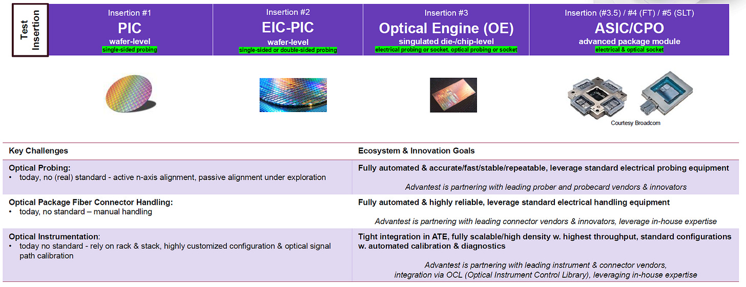
Advantest’s presentation divides the HVM test insertion points for PICs, optoelectronic devices, and CPO into several stages. The first is wafer-level testing of the photonic integrated circuit. The second is wafer-level testing of the integrated EIC-PIC structure. The third is testing of the optical engine at the singulated-die or chip level. Only after these stages does the process move to final testing or system-level testing of the advanced ASIC/CPO package.
The central objective is to establish a Known Good Optical Engine before the optical engine is integrated with the SoC. In other words, testing must be shifted left so that defective optoelectronic components can be identified before expensive packaging and system integration take place.
This is critically important for the AI semiconductor supply chain.
CPO and silicon photonics are not single-device technologies. They are highly integrated systems combining optical, electrical, thermal, mechanical, packaging, and software-control functions. Without visibility into yield at the wafer level or optical-engine level, the cost of downstream packaging failures can increase dramatically. In advanced packaging architectures such as CoWoS, EMIB, 3D ICs, and more complex xPU modules, the failure of a single optical engine could result in the loss of an entire high-value package.
This differs from the logic of conventional electrical IC testing. Traditional semiconductors can be screened progressively through wafer sort, final test, burn-in, and system-level test. In CPO, however, once optical components are integrated into the package, many defects may not be fully detectable through conventional electrical testing alone.
Optical-path loss, coupling efficiency, polarization sensitivity, temperature drift, laser stability, and fiber-alignment errors can all affect final system performance.
CPO mass production therefore requires more than simply adding another test station. It requires a fundamental redesign of the entire test insertion strategy.
Shifting Test Left: Why the Known Good Optical Engine Will Become Critical
In the era of advanced packaging, the concept of the Known Good Die has already become essential. In the CPO era, the industry will need to extend this principle to the Known Good Optical Engine.
The reason is straightforward: the more complex the package, the higher the cost of discovering failures at a later stage.
An AI accelerator package may integrate logic dies, HBM, an interposer, a substrate, a power-delivery network, a thermal solution, and optical engines. Each subsystem affects the final package yield. If an optical engine enters the packaging process without sufficient testing, defects such as excessive optical-path loss, unstable modulation performance, elevated photodetector dark current, or optical-loopback failure may only be discovered downstream, when opportunities for rework are already extremely limited.
This is why Advantest’s presentation places particular emphasis on shifting test left. The earlier a defect is identified, the lower the associated cost. The later it is discovered, the greater the financial impact.
For future AI systems, this will create a new question regarding the division of responsibilities across the supply chain: who is responsible for guaranteeing the quality of the optical engine? Is it the silicon-photonics foundry, the OSAT provider, the optical-engine vendor, the CPO switch supplier, or the hyperscaler defining and operating its own qualification framework?
This is not merely an engineering issue. It is also a commercial one.
Without common industry testing standards, each system customer may require different test items, calibration methodologies, yield definitions, and reliability conditions. This would directly increase supply-chain complexity and slow the commercialization of silicon photonics and CPO.
The future of CPO competition will therefore not be defined solely by component specifications. It will also be shaped by control over testing standards and by how responsibility for yield and quality is allocated across the supply chain.
The Three Major Gaps in SiPh/CPO Testing: Optical Probing, Connector Handling, and Automated Instrumentation
The challenge facing high-volume SiPh/CPO testing today is not a complete lack of available tools, but rather the absence of a mature and standardized ecosystem.
Advantest identified three major gaps.
First, there is still no true standard for optical probing. Current solutions continue to rely heavily on active multi-axis alignment, although passive alignment approaches are being explored.
Second, optical package fiber-connector handling remains largely unstandardized, with many processes still requiring manual intervention.
Third, optical instrumentation continues to depend heavily on rack-and-stack architectures, customized configurations, and complex optical-path calibration.

Source: Advantest
The fundamental issue is that optical testing has not yet fully adopted the operating model of semiconductor high-volume manufacturing.
Conventional IC testing emphasizes multisite testing, standardized fixtures, automated device handling, rapid calibration, and high throughput. Optical testing, however, introduces an additional layer of complexity: fibers, fiber-array units, waveguide facets, coupling efficiency, and optical-path loss can all affect measurement results.
Source: Advantest
In other words, the measured result may reflect not only the performance of the device under test, but also alignment accuracy, connector conditions, fiber-path loss, temperature drift, and calibration error.
This is one of the most difficult aspects of optical testing: the measurement system itself can easily become a significant source of error.
At the wafer-level probing stage, for example, electrical contact between the probe and the pad can be standardized relatively easily. Aligning an optical fiber with a grating coupler or edge coupler, however, requires precise control of three-dimensional positioning, angle, distance, polarization, and temperature.
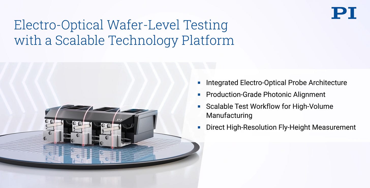
PI: Photonic wafer probing technology unifies both domains in a fully automated workflow, combining nanometer-level optical alignment with high-density electrical probing within a compact, ATE-compatible architecture. Miniaturized photonic alignment engines with precise actuation and advanced algorithms ensure stable optical coupling while sustaining production throughput. This approach reduces the cost of test through parallel workflows and offers a scalable path to high-volume manufacturing of electronic-photonic integrated circuits (EPICs).
If every test insertion requires time-consuming active alignment, high-volume manufacturing throughput will be constrained. If passive alignment is adopted instead, the optical structure, fixture tolerances, and insertion loss must all be controlled within ranges acceptable for mass production.
Similarly, once the optical engine moves into die-level or package-level testing, fiber-connector handling can become another major bottleneck. Conventional IC test equipment is highly capable of handling wafers, dies, substrates, and packaged devices, but it is not necessarily designed to manage fiber arrays, precision optical connectors, and optical-path calibration.
This means that the entire ecosystem of automated handlers, sockets, fixtures, and connectors will need to evolve.
For SiPh and CPO testing to enter true high-volume manufacturing, the industry cannot continue relying solely on laboratory-style optical measurement methods. Instead, it must build on the mature electrical IC testing ecosystem and integrate optical capabilities directly into that infrastructure.
Source: ficonTEC
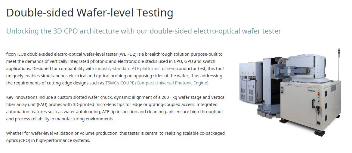
According to SemiVision’s research, wafer-level testing of a 12-inch PIC wafer can take up to 12 hours for the PIC portion alone. Developing faster and more scalable PIC testing methods will therefore be critical to determining whether silicon photonics can achieve true high-volume manufacturing.
The Essence of CPO Testing: Turning Optics into a Semiconductor Manufacturing Process
From a supply-chain perspective, competition in SiPh and CPO will not be limited to foundries, photonic chip companies, or module manufacturers. It will evolve into competition between complete testing ecosystems.
Advantest has outlined four key directions: Automation, Collaboration, Innovation, and Standardization.Its presentation clearly states that the industry needs to use standard electrical probers and handlers, combined with automation capabilities that support wafer and chip handling, as well as probecard and loadboard handling. These systems must then be integrated with standard ATE and high-density optical instrumentation to create a fully integrated test cell.
This means that the future barrier to high-volume SiPh and CPO manufacturing will shift from “Can the industry manufacture photonic chips?” to “Can photonic chips be tested using semiconductor manufacturing methods?”
This is a critical turning point for the industry.
AI infrastructure, however, demands a fundamentally different operating model. The AI supply chain requires faster production ramp-ups, greater capacity flexibility, tighter consistency, and manufacturing efficiency that is much closer to the cadence of the semiconductor industry.
The CPO testing ecosystem must therefore converge toward semiconductor manufacturing practices.
This is also an area that Taiwan’s supply chain needs to watch closely. Taiwan has world-leading capabilities in wafer fabrication, advanced packaging, IC testing, and system integration. However, optical testing, FAU alignment, optical probing, connector handling, and optical calibration standards still require much deeper ecosystem-wide collaboration.
For Taiwan to maintain a leading position in the CPO and Optical I/O era, it cannot rely solely on TSMC, packaging houses, or optical module manufacturers. It must simultaneously build integrated electro-optical testing capabilities.
Future test providers will need to measure more than conventional electrical parameters. They must also be capable of performing optical DC, electrical-to-optical, optical-to-electrical, and optical-to-optical testing, as well as modulation characterization, S-parameter measurement, optical loopback testing, and full-system functional validation.
This transformation will gradually reposition test providers from back-end subcontracting partners into an integral part of system-level yield engineering.

2025年8月20日
From Test Equipment to an Ecosystem: CPO Requires Industry-Wide Collaboration
CPO testing is not a problem that any single equipment supplier can solve independently.
A complete CPO high-volume manufacturing test cell may involve ATE, probers, handlers, probe cards, DUT boards, optical instrumentation, fiber-alignment units, connectors, sockets, software APIs, calibration models, thermal-control systems, and design-for-test architectures. Any one of these elements can become a bottleneck.
This is why Advantest emphasized in its presentation that, although SiPh and CPO are rapidly emerging, high-volume manufacturing—particularly testing—still faces numerous challenges. The industry requires close collaboration among participants across the testing ecosystem, together with full automation and interoperability among ATE, probers and handlers, probe cards and DUT boards, and auxiliary test instruments.
The significance of this statement goes beyond equipment integration. It points to a fundamental change in the industry’s collaboration model.
In conventional semiconductor testing, customers define the test specifications, ATE vendors provide the testing platform, probe-card suppliers provide the interface, and outsourced test providers execute volume production.In the CPO era, this workflow becomes considerably more complex because test results are closely linked to package design, optical-path architecture, DfT strategy, and fiber-coupling methods.
For example, if the design does not include sufficient optical loopback paths or on-chip monitors, it becomes difficult for back-end testing to quickly isolate the source of a failure. If the package-level fiber-coupling structure is not designed with high-volume testing requirements in mind, handler and socket development becomes extremely challenging. Similarly, if the instrument-control layer lacks standardized APIs, correlation between different test cells will deteriorate.
CPO production testing must therefore be considered from the earliest stages of product design.
Future DfT architectures will no longer be limited to electrical scan chains, BIST, JTAG, or memory testing. They will also need to incorporate optical DfT, optical-path calibration structures, loopback paths, monitor photodiodes, thermal sensing, and automated calibration methodologies.
As a result, CPO testing will become a jointly defined engineering discipline spanning design, manufacturing, packaging, and system integration.

The Advanced Photonics Coalition Open Ecosystem changes and grows every month. We encompass every aspect of the Silicon Photonics + Co-Packaged Optics product formation supply chain, from beginning concept to fabrication. Below is our June 2026 Open Supply Chain Ecosystem as it stands today at almost 60 members.
SemiVision Perspective: The Pace of CPO Commercialization Will Depend on Test Economics
The technological direction of SiPh and CPO is already relatively clear. However, whether these technologies can be deployed at scale in AI systems will still depend on three critical variables: yield, test time, and test cost
For AI ASICs and CPO switches, once optical components are integrated inside the package, the cost of failure becomes significantly higher than that of conventional pluggable modules. The industry must therefore establish earlier, denser, and more reliable test architectures across wafer-level, die-level, and module-level manufacturing.
This means that competition within the future CPO supply chain will not be determined solely by design and manufacturing capabilities. It will also depend on who can transform inherently unstable optical coupling into a repeatable, calibratable, and mass-producible industrial process.
As optical engines move from communications modules into AI packages, testing will no longer be merely a supporting back-end process. It will become an integral part of product definition, yield modeling, and the overall cost structure.
This reflects a much broader industry trend. AI infrastructure is bringing together three industries that were previously relatively separate: semiconductors, optical communications, and systems engineering. GPUs, ASICs, HBM, CPO, switches, substrates, optical fibers, connectors, ATE, probers, and software stacks will all become part of the same AI infrastructure optimization problem.
Within this framework, testing is not simply a cost center. It is a prerequisite for industrial scale.
Without testing, CPO will remain at the demonstration stage. Without automated testing, CPO will struggle to enter high-volume manufacturing. Without standardized testing, CPO will be unable to establish a scalable supply chain. Without a reasonable cost of test, CPO may remain commercially uncompetitive even if the underlying technology is technically viable.
In other words, the optical interconnect revolution of the AI factory era will not be driven solely by photonic chip companies, nor will it be determined exclusively by semiconductor foundries. The true inflection point will emerge only after ATE suppliers, prober and handler vendors, probe-card manufacturers, optical-instrumentation providers, packaging companies, and system customers establish common standards.
Light may enter the package, but only testing can bring light into mass production.
This is the most easily underestimated—and yet most critical—battlefield as SiPh and CPO move from concept to industrialization. On the surface, competition in future AI infrastructure appears to be a transition from electrons to photons. At a deeper level, however, the real competition is about who can first establish a CPO test interface that is manufacturable, calibratable, and scalable.
The next battle in CPO will not take place only inside photonic chips. It will also unfold across test platforms, probe cards, fiber-optic connectors, and automated test cells.
This is a battle to move from the laboratory to the factory—and from technical feasibility to industrial economics.

5月25日
Thanks for reading SEMIVISION @_@! This post is public so feel free to share it.


Previous