Beyond HBM: Samsung Targets the Next AI Battleground with Advanced Packaging and CPO
Beyond HBM: Samsung Targets the Next AI Battleground with Advanced Packaging and CPO
- Source: SemiVision
- Author: SEMIVISION
- Published: 2026-07-24T08:49:33+08:00
- URL: https://tspasemiconductor.substack.com/p/beyond-hbm-samsung-targets-the-next Beyond HBM: Samsung Targets the Next AI Battleground with Advanced Packaging and CPO


Beyond HBM: Samsung Targets the Next AI Battleground with Advanced Packaging and CPO
Original Article By SemiVision Research [Reading time: 23 mins]

Jul 24, 2026
∙ Paid
The International Conference on Electronic Packaging Technology (ICEPT) is one of the largest and most cohesive packaging technology conference in Asia. 2026 27th International Conference on Electronic Packaging Technology (ICEPT) will be held in Xi'an, China, from August 5th to 7th, 2026. The conference is hosted by Institute of microelectronics, Chinese Academy of Sciences, Xi'an Jiaotong University, IEEE-EPS and CIE-EMPT. It is organized by the School of Microelectronics of Xi'an Jiaotong University, National Center for Advanced Packaging Co., Ltd., Shaanxi Semiconductor Industry Association and Beijing Herogees Consulting Company.
Beyond HBM: Samsung Targets the Next AI Battleground with Advanced Packaging and CPO
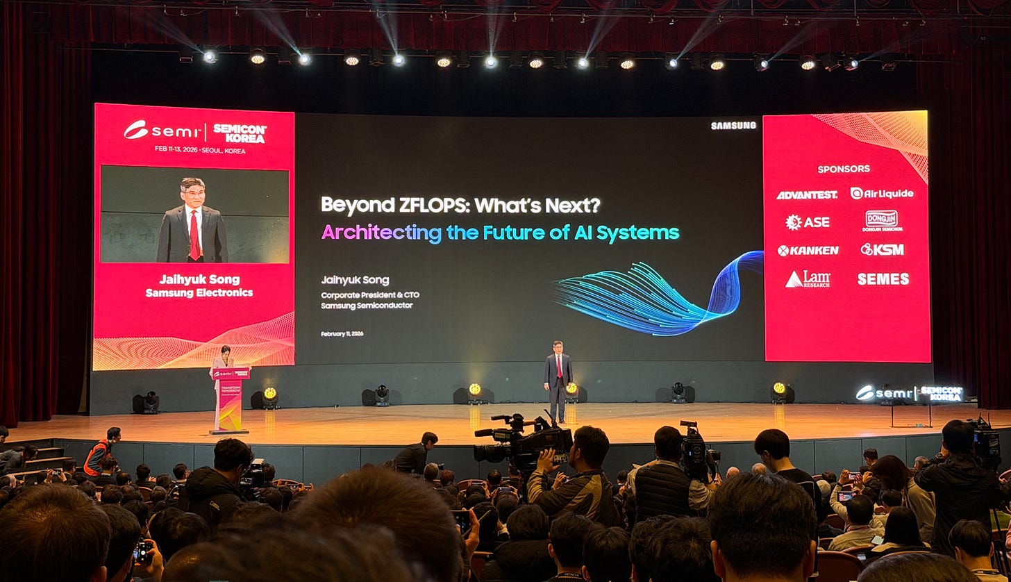
Photo by SemiVision @ Semicon Korea 2026
The AI Infrastructure Transition from Electrical to Optical Interconnects
Since the beginning of 2026, generative AI has placed rapidly increasing pressure on data-center infrastructure. As large language models scale toward the trillion-parameter level, internal data movement and energy consumption have become major constraints on further expansiormance required for training, but in deployed servers, data movement, network interconnects, and I/O power increasingly determine total system efficiency. Data-center energy studies indicate that a substantial share of server-chip power is consn. GPUs and HBM provide the floating-point perfoumed by moving data rather than by computation itself.
Against this backdrop, optical interconnects and CPO are moving from laboratory prototypes toward commercial deployment. Silicon photonics integrates optical components into wafer-scale manufacturing, allowing signals to travel through silicon waveguides at the speed of light while maintaining high bandwidth and low energy consumption over longer distances. This approach overcomes the impedance, attenuation, and crosstalk limitations of electrical transmission. Recent research suggests that placing optical I/O directly inside the processor package can reduce energy per unit of bandwidth to less than half that of current electrical interfaces while delivering stable, nanosecond-class latency across server racks.
4月25日
The nature of AI workloads is also changing. Training emphasizes high-throughput, matrix-intensive computation, whereas inference—especially the decode stage—depends heavily on memory access and low-latency sequential processing. This shift has created demand for new inference accelerators such as the LPU. LPUs combine large amounts of on-chip SRAM with deterministic execution, using chip-wide communication and high-speed SRAM access to minimize latency while generating large numbers of tokens per second. The Groq 3 LPU and the Rubin + LPX architecture announced at NVIDIA GTC 2026 illustrate how rapidly the inference market is expanding and why it may soon surpass the training market.

This article provides an in-depth analysis of Samsung Electronics’ strategy to combine advanced packaging, silicon photonics, and CPO to build an LPU inference foundry business and a broader AI infrastructure platform. Drawing on SemiVision research and other public information, it examines the technical architecture, industry landscape, competitive advantages, and execution risks behind Samsung’s next move: avoiding the crowded GPU + HBM battlefield and opening a new AI growth path through LPU inference, co-packaged optics, and a more complete ecosystem.
Below we will share:
The Rise of Silicon Photonics and Co-Packaged Optics
Current Status and Outlook for Co-Packaged Optics
Samsung’s 300 mm Silicon-Photonics Platform
Production Road Map and Competitive Strategy
Advanced Packaging: Breakthroughs in Hybrid Copper Bonding and HBM
Groq’s LPU Architecture and the Rapid Expansion of the Inference Market
Samsung’s Integrated Strategy

7月2日
The Rise of Silicon Photonics and Co-Packaged Optics: Solving the Data-Movement Bottleneck
The Limits of Electrical Interconnects and the Advantages of Optical Links
Conventional electronic systems use copper traces and printed circuit boards to move data between chips. As signaling frequencies rise into the hundreds of gigahertz, attenuation, reflections, and crosstalk deteriorate rapidly, requiring extensive transmitter and receiver equalization and driving a disproportionate increase in power consumption. High-speed electrical links must also remain short. Once a server system scales to hundreds or thousands of GPUs, optical fiber becomes unavoidable. Research institutions have highlighted that optical interconnects can provide longer reach, higher bandwidth density, lower power consumption, and lower latency. In AI and machine-learning systems in particular, enormous volumes of data must move rapidly between chips, making data-transfer energy one of the dominant contributors to server-chip power.
Silicon photonics uses CMOS-compatible silicon or silicon-nitride waveguides to form optical paths on a chip, with external or integrated light sources generating and transmitting optical signals. Photonic integrated circuits can be manufactured at scale and at substantially lower cost than platforms based on III-V materials such as gallium arsenide. On a 300 mm wafer, developers can integrate optical modulators, waveguides, photodiodes, splitters, and microring resonators. This monolithic optical integration is the foundation of co-packaged optics.
Co-packaged optics integrates optical engines or transceivers directly into the package of a logic chip, converting electrical signals into optical signals over extremely short, millimeter-scale distances. The architecture offers several advantages:
Lower power and higher bandwidth density: CPO can eliminate part of the SerDes receiver path used by conventional pluggable optical modules, shortening the electrical channel and reducing power consumption. Power is expected to fall to roughly one-third that of traditional optical transceivers. Fiber can also exit directly from the package, sharply increasing the amount of bandwidth that can be delivered per unit of area.
Lower latency: Optical fiber can remove the delay associated with long electrical traces and reduce the need for complex DSP compensation. In practice, CPO can reduce latency from tens of nanoseconds to only a few nanoseconds.
Greater system disaggregation: With co-packaged optics, GPUs, CPUs, and LPUs can be connected by fiber across different racks or even different data centers, substantially improving system scalability. Ayar Labs’ UCIe-compatible TeraPHY optical chiplet can provide 8 Tb/s of bandwidth and maintain stable transmission from meter-scale to kilometer-scale distances, enabling chiplets from different vendors to interoperate through the UCIe standard.
Current Status and Outlook for Co-Packaged Optics
Despite its strong technical advantages, CPO remained limited to pilot programs at a small number of companies before 2026. Most data centers still use pluggable optical transceivers connected through printed circuit boards because thermal management, manufacturing complexity, and the optical-module supply chain are not yet fully mature. External research has identified 2026 as a potential inflection point for CPO production, with global penetration projected to reach 35% by 2030. Broadcom and NVIDIA are exploring CPO links between switches and processors; TSMC has introduced its COUPE platform for CPO services; and Intel, GlobalFoundries, and start-ups including Ayar Labs, Celestial AI, and Lightmatter are developing optical chiplets and interconnect specifications.
From SemiVision’s perspective, CPO is no longer a competition among individual components; it is a competition among platforms. Silicon-photonics foundry services, optical-chiplet design, packaging technology, and system integration are all essential. Ayar Labs, for example, is working with OSAT providers to establish high-yield production lines while promoting cross-vendor interoperability through UCIe. Samsung’s strategy combines a 300 mm silicon-photonics platform, advanced packaging, and hybrid copper bonding in an effort to build an end-to-end CPO supply chain.
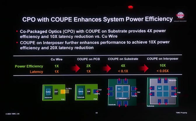
Source: TSMC
Samsung’s 300 mm Silicon-Photonics Platform: From Laboratory Development to Volume Production
The Silicon-Photonics Foundry Platform Unveiled at OFC 2026
At the OFC in March 2026, Samsung formally announced its entry into the silicon-photonics foundry market. The platform uses a 300 mm CMOS process, allowing equipment and manufacturing infrastructure to be shared with existing logic processes, lowering cost and improving reliability.

Source: Samsung
Samsung’s 300 mm silicon-photonics platform includes a complete process design kit supporting high-speed modulators, high-speed photodetectors, passive optical waveguides, silicon-nitride (SiN) waveguides, through-silicon vias, and bump packaging. Customers can therefore design an entire photonic integrated circuit on a 300 mm wafer and co-manufacture it with logic, rather than sourcing only isolated optical devices.
Key technical features of Samsung’s platform include:
Multi-step etched silicon and silicon-nitride waveguides: The platform uses stepped etching in a 305 nm silicon layer and a 400 nm silicon-nitride waveguide layer to reduce propagation loss and support multiple optical modes. Test results indicate silicon-waveguide loss of approximately 1.2 dB/cm and silicon-nitride waveguide loss of approximately 0.4 dB/cm.
High-speed modulators and photodetectors: The platform supports PN-doped Mach-Zehnder interferometer modulators and microring modulators. The microring modulator delivers modulation efficiency of 52 pm/V with 0 dB insertion loss and a bandwidth of 74 GHz, while the MZI modulator reaches 50 GHz. Germanium photodiodes can also be configured as high-gain avalanche photodiodes.
A comprehensive PDK and device library: Samsung’s PDK provides more than 40 device models covering refractive-index behavior, free-carrier absorption, thermal effects, and other parameters. It also includes reference designs and support for Verilog-A and photonic simulation, allowing designers to perform joint electronic-photonic co-design within an EDA environment.
Samsung also demonstrated a 224 Gb/s-per-lane silicon-photonic modulator targeting 800G and 1.6T optical modules. These devices are intended not only for standalone transceivers but also as building blocks for on-package optical engines in future CPO platforms.
Production Road Map and Competitive Strategy
Samsung has published not only the platform itself but also a full commercialization road map:
2027: Launch optical engines using thermal compression bonding. TCB is already widely used in HBM packaging and can support 2.5D integration at relatively low cost.
2028: Introduce hybrid copper bonding to achieve finer interconnect pitches. HCB bonds copper directly to copper without solder bumps, increasing vertical interconnect density and thermal efficiency. Samsung expects HCB to enable tighter integration between optical engines and logic dies while improving yield.
2029: Offer a complete turnkey CPO service. Samsung plans to combine its silicon-photonics platform, advanced packaging, and HCB so customers can complete chip design, wafer fabrication, and optical-engine packaging through a single supplier.
In the competitive landscape, TSMC has taken an early lead with pilot production using COUPE, its Co-Packaged Optical Unified Platform Ecosystem, and has targeted CPO volume production in 2026.

Samsung is entering through its strengths in memory and foundry manufacturing, emphasizing a four-in-one model of memory + advanced packaging + silicon photonics + foundry services. Its objective is to offer a more complete solution than logic manufacturing alone.
GlobalFoundries has also acquired AMF’s silicon-photonics production line in Singapore and plans to launch a 300 mm platform. Industry analysis increasingly suggests that future competition in silicon photonics will center on platform capability rather than individual devices.
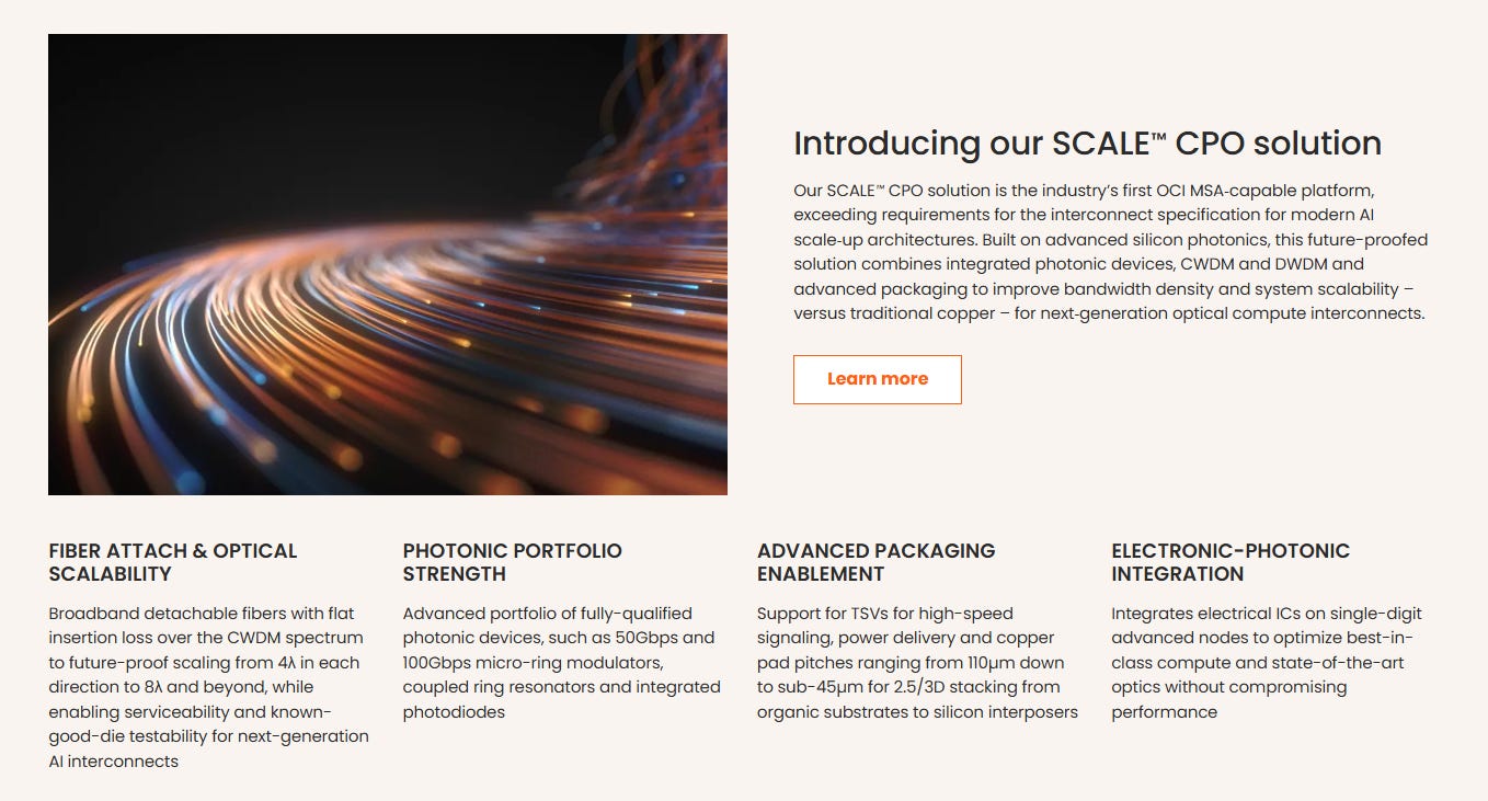
Singapore R&D Center and International Collaboration
To accelerate the development and adoption of silicon photonics, Samsung announced a new R&D center in Singapore in 2026, reportedly led by a former senior TSMC executive and working with organizations such as A*STAR.
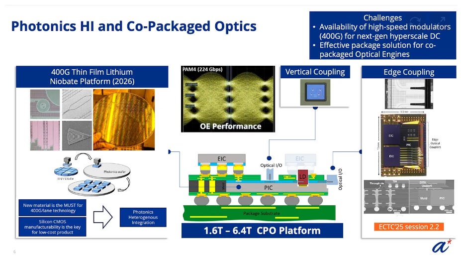
The center provides Samsung with an Asian talent base while complementing Singapore’s advanced-manufacturing assets, including the capabilities built around AMF. Samsung is also collaborating with major optical-networking companies such as Broadcom to develop modules and strengthen the ecosystem around its platform.

7月15日

2025年6月21日
Advanced Packaging: Breakthroughs in Hybrid Copper Bonding and HBM
How HCB Works and Why It Matters
Hybrid copper bonding is one of Samsung’s core advanced-packaging development programs. Conventional thermal compression bonding uses solder microbumps and an adhesive interface to connect dies to an interposer. However, interconnect pitch is constrained by solder-ball dimensions, and thermal resistance remains relatively high. As die stacks become taller, heat dissipation and signal integrity become bottlenecks. HCB instead directly bonds pretreated copper surfaces, creating a metal-to-metal connection between dies. Samsung says HCB can enable HBM stacks beyond 16 layers and reduce thermal resistance by more than 20%, making it better suited than TCB for advanced HBM.

In 2026, Samsung’s semiconductor division established an HCB production line in Cheonan for advanced memories including HBM4, HBM4E, and HBM5. HCB requires exceptional cleanliness and surface planarity, so production depends on highly precise chemical-mechanical polishing and cleaning processes. Unlike non-conductive film (NCF, Resonac) bonding, HCB is a fluxless process, avoiding residues that could reduce long-term reliability. HCB also supports much finer interconnect pitches, potentially below 2 micrometers, making it suitable for ultra-high-density 3D stacking and hybrid photonic-electronic packaging.
Complementary Roles for HBM4/HBM4E and System Memory
HBM and DDR5/DDR6 will continue to coexist in the data-center memory market. Groq’s LPU uses a large amount of on-chip SRAM to reduce latency, but servers must also support CPUs, BlueField DPUs, and other components, meaning large systems still require external DDR memory. LPX systems are therefore expected to use a three-tier memory hierarchy of SRAM + HBM + DDR. Samsung’s HBM4E, built with HCB, can support higher stacking density. As LPX assigns the decode workload to LPUs, some bandwidth demand may shift away from HBM, potentially benefiting DDR. Samsung can use its broad memory portfolio to provide comprehensive support for LPU inference and create product-level synergies.
Where Advanced Packaging and CPO Converge
Co-packaged optics requires optical engines to be installed very close to logic dies, creating new packaging requirements:
Greater layout flexibility: By eliminating solder bumps, HCB allows optical-engine chiplets to be placed closer to logic dies, shortening the electrical-to-optical conversion path and improving heat dissipation.
Large interposers: CPO commonly uses 2.5D packaging with large silicon or organic interposers that may exceed 2,000 mm2. Samsung’s advanced-packaging portfolio includes RP (Redistribution Package), I-Cube, and X-Cube, supporting large substrates and 3D stacking.
Fiber-interface packaging: CPO must route fiber into the package and align it with optical waveguides, requiring micromirrors and fiber arrays. Samsung can mount silicon-photonic dies on a base substrate through TCB or HCB and couple fiber through microlenses or etched silicon structures.
Because these requirements are highly complex, Samsung’s combination of advanced-packaging resources and foundry experience gives it a meaningful competitive position in the global silicon-photonics and CPO markets.

Source: ASE
ASE: Advanced Packaging Evolution: Chiplet and Silicon Photonics-CPO
Groq’s LPU Architecture and the Rapid Expansion of the Inference Market
The LPU Design Philosophy
Groq specializes in AI inference accelerators. Its founder, Jonathan Ross, previously led Google’s TPU team before establishing Groq in 2016. The LPU follows a software-first design philosophy, using a simplified instruction set and deterministic execution to minimize latency. A programmable tensor-streaming pipeline defines the execution path in advance, relying on static scheduling to eliminate the unpredictable latency and resource contention associated with GPU execution.

The first-generation LPU, known as GroqChip or TSP, was manufactured on a 14 nm process and contained approximately 5,120 vector arithmetic units, 230 MB of on-chip SRAM, and 80 TB/s of internal bandwidth. Because it did not use HBM, model weights could be stored in on-chip SRAM and accessed at full bandwidth during inference. Groq claimed energy consumption of only 1-3 joules per generated token, compared with roughly 10-30 joules for GPUs at the time.
The second-generation LPU was manufactured by Samsung Foundry on its 4 nm SF4X process. Samsung and Groq announced their collaboration in 2023. The chip uses a next-generation TSP architecture designed to increase throughput, reduce latency and power, and scale systems from approximately 85,000 chips to more than 600,000. This reflects the LPU’s ability to form very large clusters through direct chip-to-chip interconnects without relying on external switches.

3月30日
Groq 3 LPU and the LPX System
In March 2026, NVIDIA and Groq jointly introduced the Groq 3 LPU and the LPX architecture paired with Rubin GPUs at GTC. Groq 3 is manufactured on Samsung’s 4 nm SF4X process, contains 9.8 billion transistors, integrates 500 MB of on-chip SRAM, and provides total memory bandwidth of 150 TB/s—about seven times the roughly 22 TB/s associated with HBM4. One LPX rack uses 256 Groq 3 LPUs, providing 128 GB of aggregate SRAM and 40 PB/s of on-chip bandwidth. The LPX accelerator handles the decode stage of language-model inference, while Rubin GPUs continue to perform training and prefill. This heterogeneous architecture can increase inference throughput per watt by as much as 35 times, reduce latency, and potentially unlock ten times more revenue from trillion-parameter models.
Groq 3’s deterministic execution is particularly important for agentic AI and real-time conversational applications. Unlike the out-of-order execution behavior of GPUs, the LPU can maintain stable per-token latency regardless of workload variation. This is a critical capability for the emerging agentic-computing era. Market forecasts suggest that inference could account for roughly two-thirds of AI compute demand around 2026, positioning the LPU as a prominent architecture in the inference era.
Why Groq Chose Samsung Foundry
Many observers have asked why Groq selected Samsung Foundry rather than TSMC. Several factors may explain the decision:
Process capability and capacity availability: Groq 3 uses Samsung’s 4 nm SF4X process and requires efficient SRAM integration with high-speed logic. Reports in 2026 indicated that Samsung’s 4 nm yield had improved to approximately 80% and that volume production of Groq’s third-generation LPU had been validated. At the same time, TSMC’s 3 nm and 2 nm capacity was heavily allocated to high-margin GPU programs, potentially making it more difficult for Groq to secure sufficient capacity.
Using SRAM instead of HBM to avoid packaging bottlenecks: To achieve low latency, Groq 3 relies on large amounts of SRAM rather than HBM. It therefore does not require a large silicon interposer or CoWoS packaging and can reach high performance with a less complex advanced-package architecture. Samsung already offers mature platforms such as I-Cube and X-Cube and is investing heavily in HCB, creating a path toward future integration with optical engines.
Alliance and ecosystem considerations: NVIDIA entered into a licensing arrangement with Groq in 2025 and integrated Groq LPUs into the Rubin architecture as decode accelerators. At GTC 2026, NVIDIA CEO Jensen Huang publicly thanked Samsung for manufacturing Groq 3. For Groq, Samsung provides not only process technology but also access to memory and advanced-packaging integration, supporting the construction of a more complete AI platform.
Samsung’s Integrated Strategy: Combining Memory, Foundry, Advanced Packaging, and CPO
The Four-in-One Advantage: Memory + Silicon Photonics + Packaging + Foundry
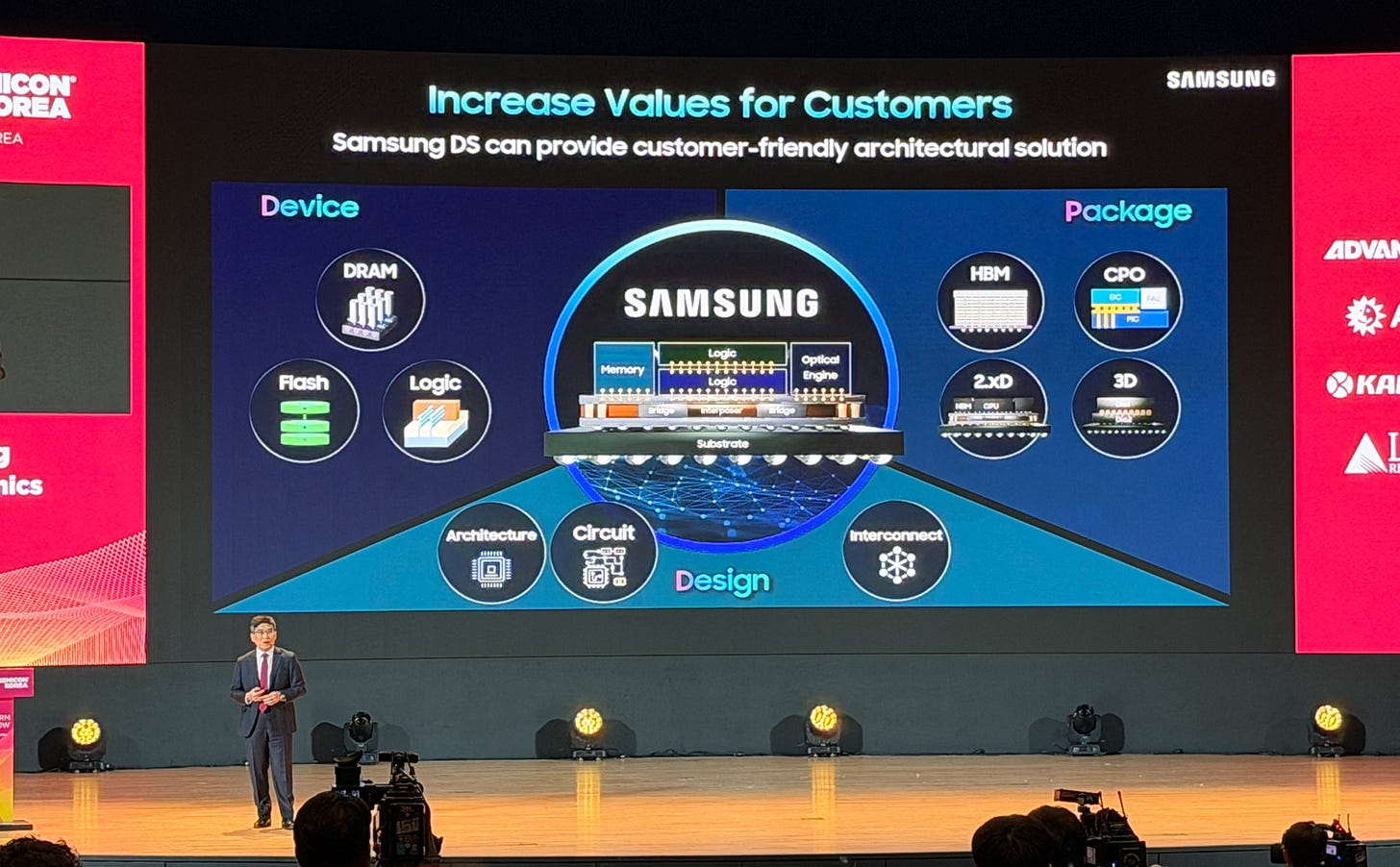
Photo by SemiVision @ Semicon Korea 2026
Samsung Electronics controls a broad value chain spanning DRAM and NAND memory, wafer foundry services, advanced packaging, and silicon photonics. In the AI data-center market, this vertical integration can create several forms of synergy:
Memory and storage: Samsung is a major supplier of HBM and DDR5/DDR6. Its HBM4 and HBM4E products, combined with HCB, can support stacks beyond 16 layers while reducing thermal resistance. At the system level, AI servers also require NVMe SSDs, another market in which Samsung holds a strong enterprise position.
Silicon photonics and CPO: By combining a 300 mm silicon-photonics platform with future CPO integration, Samsung can offer a coordinated photonic-electronic solution. Partnerships with networking companies such as Broadcom and Cisco can accelerate its entry into the optical-interconnect market for AI data centers.
Advanced packaging and HCB: Samsung has already introduced I-Cube and X-Cube for 2.5D packaging and is developing HCB to increase vertical interconnect density. CPO requires an extremely short electrical path between optics and logic, together with effective thermal management. Solder-bump-free HCB can help deliver both low thermal resistance and high-performance interconnects.
Wafer foundry: Samsung Foundry can manufacture AI accelerators on SF4X and future 3 nm and 2 nm processes. Although its market share remains below TSMC’s, its cost-performance proposition and process reliability have improved, and its technologies have been adopted by companies including NVIDIA, IBM, and Baidu.
By integrating these four capabilities, Samsung is attempting to build a one-stop solution spanning chips, packaging, optical interconnects, and system-level products. The objective is no longer simply to supply individual AI chips, but to control a critical entry point into the next generation of AI infrastructure.
Strategic Alignment with CPO
Commercial CPO requires optical engines and logic dies to be packaged together. Samsung plans to launch TCB-based optical engines first, move to more compact HCB-based optical engines in 2028, and provide a complete CPO service in 2029. During this transition, demand for LPU inference could support early production of silicon-photonics wafers and optical engines. The Groq-Samsung relationship may create a first-mover advantage: LPUs combine large SRAM arrays with deterministic execution and therefore require low-latency chip-to-chip interconnects, an ideal use case for silicon-photonic chiplets. Once the photonics platform is established, future LPU generations could integrate optical I/O to connect LPUs with Rubin GPUs or with other LPUs at much greater scale.
CPO can also move server-to-server interconnects from on-board copper to optical fiber. This would allow LPUs and GPUs to connect across racks or even across data halls, creating disaggregated AI clusters. Such disaggregation is important for AI cloud services because different models and workloads may require dynamic allocation among different types of accelerators.

6月18日
Competitive Landscape: Samsung versus TSMC, GlobalFoundries, Intel, and Start-ups
The principal competitors in silicon photonics and CPO include TSMC, GlobalFoundries, Intel, and Ayar Labs. TSMC is working with Broadcom through its COUPE platform and has targeted volume production of CPO switch modules in 2026, building on its leadership in advanced process technology and packaging. GlobalFoundries acquired AMF’s silicon-photonics business in Singapore to build a 300 mm platform serving optical-connectivity and data-communications customers. Intel demonstrated modular optical I/O in 2023 and has targeted pluggable optical-I/O chiplets, allowing servers to adopt optical connectivity in a modular way.
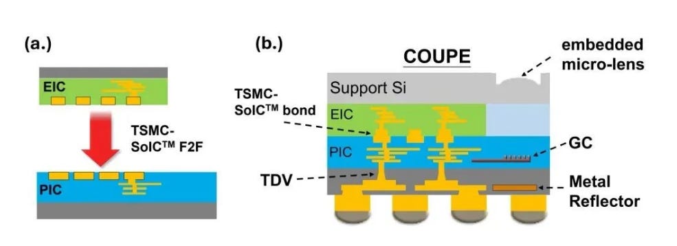
Source: TSMC
Among start-ups, Ayar Labs has developed the microring-based TeraPHY optical chiplet, which provides 8 Tb/s of bandwidth and can connect multiple accelerators so they behave like a single large GPU. The company is working with OSAT providers to establish a CPO production line. Celestial AI is developing its Photonic Fabric to bring photonics into the AI memory fabric, while Lightmatter emphasizes photonic matrix computation. These companies typically rely on large foundries to manufacture their optical chiplets, but their smaller scale could also make them future acquisition targets.
4月2日
Samsung, by comparison, can offer customers a more complete supply chain through its memory capacity and advanced-packaging technologies. Its HCB and optical-packaging capabilities provide differentiation in CPO. However, TSMC’s lead in advanced logic and 3D integration continues to give it a larger position in the high-end market. Competition between the two may ultimately depend on which company can commercialize CPO and silicon-photonics platforms faster and build the broader ecosystem.
SemiVision’s View: Samsung’s Optical-Interconnect + Inference Strategy
SemiVision’s analysis of Samsung’s silicon-photonics and CPO strategy argues that the company’s real bet is on the optical-interconnect layer of next-generation AI data centers, not on standalone silicon-photonic components. The main conclusions are as follows:
Platform competition, not component competition: Silicon photonics previously remained largely at the laboratory stage, with vendors supplying individual modulators or photodiodes. Samsung’s 300 mm platform unveiled at OFC 2026 is a complete foundry offering that includes a PDK, a device library, TSV integration, and packaging. This indicates that silicon photonics is entering a platform-competition phase.
AI data centers are moving from the GPU era toward the CPO era: The bottleneck is shifting from raw GPU compute to data movement and network interconnects. Future AI-server competition will be a system-level contest across GPU + network + optical I/O + packaging. Silicon photonics could become as strategically important as HBM.
The rise of LPU inference: By using SRAM instead of HBM, LPUs can avoid current constraints in HBM supply and CoWoS capacity. Groq 3’s 500 MB of SRAM supports strong decode performance. More importantly, LPUs can divide workloads with GPUs, NPUs, and ASICs to create heterogeneous accelerator systems. Samsung’s decision to manufacture LPUs allows it to avoid the crowded GPU market and enter a new inference-computing segment.
Silicon-photonics integration and the CPO road map: Future AI clusters will extend optical connectivity from GPU-to-GPU links to rack-to-rack, cluster-to-cluster, and eventually data-center-to-data-center connections. Silicon photonics, CPO, and optical I/O will become progressively more important. Samsung’s early investment in a 300 mm SiPh platform and CPO is intended to secure a strategic entry point into this networking transition.
Integrated capability will matter more than any single technology: Future competition will not be determined by advanced process nodes alone, but by the combined strength of foundry manufacturing + packaging + silicon photonics + ecosystem development. Samsung, TSMC, Intel, and GlobalFoundries each have different platform advantages, but leadership in CPO, silicon photonics, inference foundry services, and system integration will determine who controls the next generation of AI infrastructure.
Customers and Ecosystem: Building an Optical-Interconnect Network from Groq to Broadcom
Groq and NVIDIA: A Model for Heterogeneous Inference Collaboration
The Rubin + LPX architecture developed by NVIDIA and Groq demonstrates the potential of GPU-LPU collaboration. Rubin GPUs handle prefill and attention-intensive computation, while LPX performs the decode stage of sequence generation. High-speed interconnects and coordinated software enable dynamic scheduling at the bare-metal level. This division of labor increases inference speed and reduces total power consumption. At GTC 2026, NVIDIA CEO Jensen Huang publicly thanked Samsung for manufacturing the Groq 3 LPU. The alliance suggests that future semiconductor partnerships will increasingly cross the traditional boundaries between process technology and system architecture.
Networking Leaders Including Broadcom and Cisco
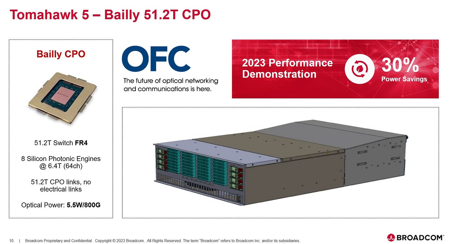
Broadcom was among the earliest networking companies to promote CPO, and itsTomahawk 5 switchhas been tested with Ayar Labs optical chiplets. Samsung plans to work with Broadcom, Cisco, and other networking vendors to apply its 300 mm silicon-photonics platform to the foundry production and packaging of optical engines and photonic switch ASICs. Such partnerships would give Samsung access to the data-center networking ecosystem, help validate CPO-module performance, and provide valuable customer feedback.
Start-ups and Research Institutions
In addition to collaborating with large companies, Samsung has established an R&D center in Singapore and is working with A*STAR and academic institutions on silicon-photonic devices and talent development. Samsung could also cooperate with start-ups developing optical chiplets, including Ayar Labs and Celestial AI, and use standards such as UCIe to connect those chiplets with Samsung Foundry’s silicon-photonics platform, expanding the ecosystem around its technology.
Technical Challenges and Execution Risks
Although optical interconnects and LPU inference offer significant growth potential, Samsung still faces several major execution challenges:
Thermal management and reliability: CPO places light sources and optical modules close to high-power logic dies. Ensuring the long-term stability of lasers or microLEDs in this thermal environment is difficult. Packages will require lower-thermal-resistance materials and dynamic thermal-control mechanisms.
Manufacturing complexity and cost: Although silicon-photonics wafer processes are compatible with CMOS infrastructure, optical coupling, alignment, and packaging are extremely complex and can create yield problems. HCB also requires precise control of surface planarity and cleanliness. The large up-front investment required for development and production ramp-up could weigh on near-term profitability.
Ecosystem maturity: CPO benefits can be realized only when networking equipment, servers, and the software stack are integrated as a complete system. A lack of standardization can make early systems difficult to interoperate. Samsung must work with standards and ecosystem initiatives such as UCIe, COUPE, and CXL to enable cross-vendor compatibility.
Market acceptance and competitive pressure: Pluggable optical transceivers are already deeply established in data centers. A broad transition to CPO would require much of the supply chain to be rebuilt, and customers may remain concerned about cost, serviceability, and repair. TSMC, Intel, and multiple start-ups are competing aggressively. If Samsung cannot establish a clear lead quickly, it could lose its window of opportunity.
Forward Outlook: AI Infrastructure from 2026 to 2030
As generative AI continues to expand, inference demand could overtake training demand over the next several years. The heterogeneous LPU + GPU architecture emerging in 2026 may influence data-center design for the next decade. At a high level, future AI infrastructure is likely to evolve along four major directions:
A more diverse memory hierarchy: Future AI accelerators will use multiple memory tiers, including on-chip SRAM, HBM, DDR, and NAND. The emergence of the LPU highlights the renewed importance of SRAM, but SRAM will not replace HBM. Each memory type will serve different workload requirements within a coordinated hierarchy.
Optical interconnects become mainstream: CPO and optical chiplets will extend from switches into processors. Future data centers may adopt optical switching architectures that allow GPUs and LPUs across multiple racks to exchange data at extremely high speed with lower energy per bit.
Heterogeneous computing and workload specialization: Rubin GPU + Groq LPU is an early example. More specialized AI chips may emerge, including Transformer accelerators, edge NPUs, and search-engine ASICs. Foundries will therefore need to offer a wider range of process and packaging options that allow different chip types to operate together.
Standardization and modularity: Standards such as UCIe, CXL, and COUPE will promote interoperability among chiplets and allow system vendors to assemble systems from modular components. Samsung’s silicon-photonics and advanced-packaging platforms must support these standards to remain competitive within the broader ecosystem.
Conclusion: Samsung’s Future and the Industry Implications
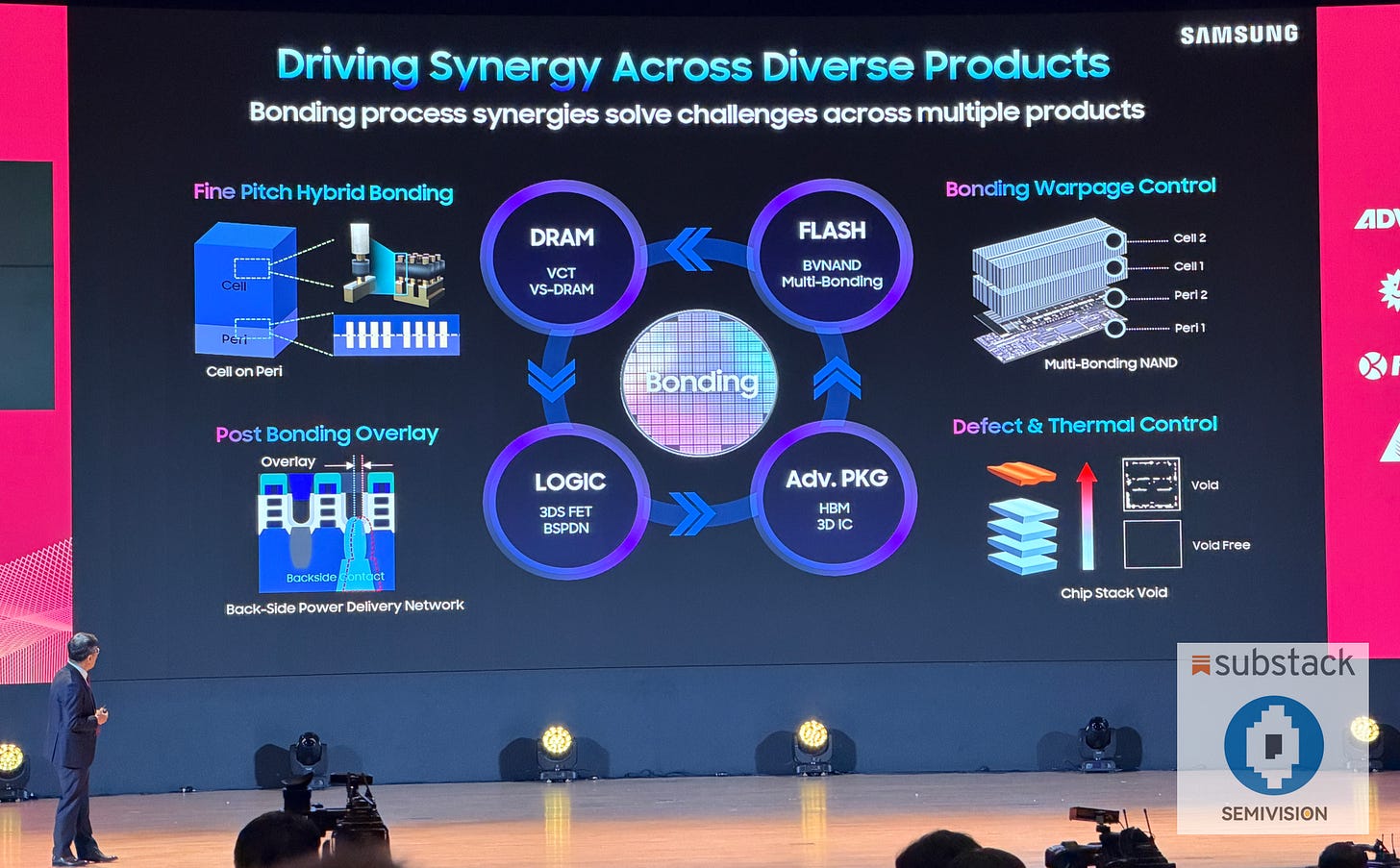
Photo by SemiVision @ Semicon Korea 2026
Samsung Electronics is using its accumulated strengths in memory, packaging, and foundry manufacturing to make a broad strategic bet on optical interconnects + inference. Through its 300 mm silicon-photonics platform, hybrid copper bonding, HBM4/HBM4E memory, and LPU foundry services, Samsung aims to offer an integrated AI solution spanning chip design, fabrication, packaging, optical modules, and system integration. The strategy is designed to move beyond the crowded GPU market and position Samsung at the center of the transition toward the CPO era.
Execution will not be easy. Samsung must still overcome commercialization challenges, competition from TSMC and other major players, and the need to build standards and an ecosystem. Over the next several years, the company that first commercializes silicon-photonic CPO and LPU solutions at scale could secure a critical entry point into AI data centers. For industry participants and investors, the direction is already clear: optical interconnects, advanced packaging, and heterogeneous acceleration are reshaping semiconductor competition. Samsung’s strategy may be less about simply catching TSMC and more about creating a new market position of its own.
Thanks for reading SEMIVISION @_@! This post is public so feel free to share it.

5月13日


PreviousNext