TSMC’s $100 Billion Arizona Bet Is Reshaping the Global Chip Supply Chain
TSMC’s $100 Billion Arizona Bet Is Reshaping the Global Chip Supply Chain
- Source: SemiVision
- Author: SEMIVISION
- Published: 2026-07-22T09:52:53+08:00
- URL: https://tspasemiconductor.substack.com/p/tsmcs-100-billion-arizona-bet-is TSMC’s $100 Billion Arizona Bet Is Reshaping the Global Chip Supply Chain


TSMC’s $100 Billion Arizona Bet Is Reshaping the Global Chip Supply Chain
Original Article by SemiVision Research [Reading time: 13 mins]

Jul 22, 2026
TSMC’s $100 Billion Arizona Bet Is Reshaping the Global Chip Supply Chain
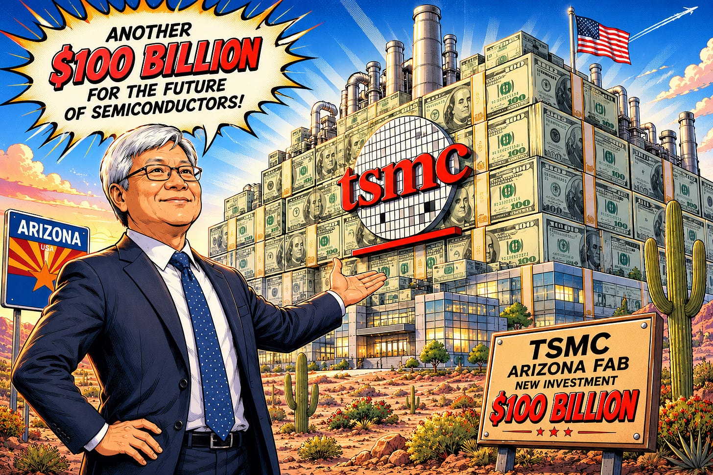
AI Is Turning Semiconductor Manufacturing into Strategic Infrastructure—and Customers Will Ultimately Pay the Bill
If the semiconductor story from 2023 through 2025 was defined by the explosive growth of artificial intelligence, the central question for 2026 is becoming more difficult:
Who will pay for the reconstruction and geographical duplication of the advanced semiconductor supply chain?
TSMC’s second-quarter earnings call on July 16 provided a clear, if uncomfortable, answer. The cost will eventually be distributed across chip designers, cloud service providers, equipment makers, materials suppliers, governments—and ultimately the companies and consumers purchasing AI computing services.
The scale is extraordinary, but the strategic message is even more important.
AI is no longer creating only a temporary demand surge for GPUs. It is transforming the leading-edge semiconductor supply chain into a long-cycle, capital-intensive and geopolitically managed infrastructure system.
The era of manufacturing advanced chips almost entirely where production was most efficient is gradually ending. What is replacing it will be more geographically distributed, more politically acceptable—and considerably more expensive.
The Financial Numbers Reveal a Structural Shift
TSMC’s quarterly performance shows why management is prepared to make such an aggressive commitment.
Second-quarter revenue reached $40.2 billion, while gross margin climbed to 67.7%. High-performance computing increased 20% sequentially and accounted for 66% of quarterly revenue. Technologies at 7 nanometers and below represented 77% of wafer revenue, while the newly ramping 2-nanometer process already contributed 3%.

These numbers indicate that TSMC’s growth is increasingly concentrated in the most capital-intensive part of semiconductor manufacturing.
The company said that approximately 70% to 80% of its 2026 capital budget would be allocated to advanced process technologies. Another 10% to 20% would be directed toward advanced packaging, testing, mask making and related capabilities. TSMC also stated that capital expenditure over the next three years would be “even more significantly higher” than during the previous three-year period.
This is not normal capacity expansion.
It is the industrialization of AI infrastructure at semiconductor scale.
The semiconductor industry previously relied on relatively predictable product cycles. Smartphone processors, PCs and consumer devices created large but generally understandable demand patterns. AI changes that planning model because demand is being driven not only by unit shipments but by an expanding requirement for computation, memory bandwidth, networking capacity and power.
Each new generation of AI accelerator also requires more than a smaller transistor.
It requires a larger silicon area, more advanced packaging, additional HBM stacks, more complex substrates, higher-speed interconnects, more sophisticated thermal materials and significantly greater power-delivery capacity. As a result, semiconductor capital intensity is expanding faster than wafer demand alone would suggest.

6月30日
Arizona Is Not Simply Another Fab Location
The simple interpretation of TSMC’s announcement is that the company is expanding because AI demand is strong.
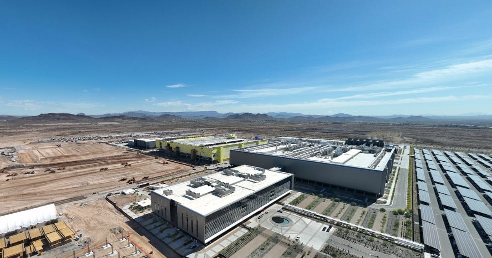
TSMC Arizona / Source: TSMC
That is correct, but incomplete.
Arizona represents something fundamentally different from an ordinary offshore manufacturing investment. It is becoming part of a politically acceptable domestic supply route for U.S. cloud providers, AI chip companies and government-linked customers.
TSMC said the new investment would support several additional logic fabs using 2-nanometer and more advanced technologies, together with advanced packaging capacity. Management indicated that four or more additional front-end and back-end facilities could eventually be built, although the timing would depend on market conditions.
5月8日
The inclusion of advanced packaging is critical.
Producing wafers in the United States but shipping them back to Asia for packaging would leave a major part of the AI supply chain outside the country.AI accelerators are not complete products when the wafer leaves the front-end fab. Their commercial value emerges only after logic dies, HBM, interposers, substrates, power-delivery structures and thermal interfaces are assembled and tested as an integrated system.
For the United States to claim a more complete domestic AI semiconductor chain, it needs more than leading-edge lithography. It also needs advanced packaging, test capacity, substrates, memory integration, chemicals, specialty gases, equipment maintenance and a qualified engineering workforce.
Earlier U.S. semiconductor programs had already begun supporting this broader ecosystem. Projects involving Amkor, SK hynix, Absolics and other suppliers targeted domestic advanced packaging, HBM-related development and next-generation substrate technologies. TSMC’s newest announcement reinforces the direction of travel: U.S. semiconductor policy is moving from subsidizing isolated fabs toward constructing a more complete manufacturing cluster.
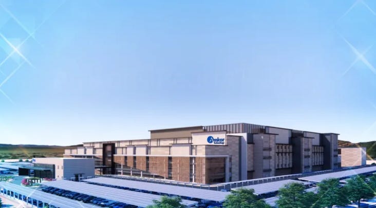
Source: Amkor
Amkor has begun construction on a new semiconductor packaging and testing campus in Peoria, Arizona, representing a rare U.S. capacity expansion in one of the industry’s most strategically important and supply-constrained segments. The campus will include multiple buildings and as much as 750,000 square feet of cleanroom space. The first factory is expected to be completed by mid-2027, with commercial production scheduled to begin in early 2028.
Apple and Nvidia have already been identified as the project’s initial anchor customers. The facility will provide advanced packaging services for Apple silicon manufactured at TSMC’s nearby Arizona fabs, creating a more localized front-end and back-end semiconductor supply chain within the state.
The U.S. Department of Commerce previously announced up to $400 million in proposed CHIPS Act funding for the project, describing it as the largest outsourced advanced packaging facility in the United States. The initial development phase represents an investment of approximately $2 billion. Arizona officials, however, expect the site to expand over time into a campus worth as much as $7 billion, potentially supporting up to 3,000 jobs.
The Emergence of a Localization Premium
For decades, foundry pricing primarily reflected process complexity, yield, depreciation, utilization and competitive conditions.
Future pricing will need to reflect more.
Overseas fabs involve higher labor expenses, duplicated infrastructure, smaller initial production scale and less concentrated supplier networks. TSMC said the ramp-up of overseas facilities was expected to dilute gross margin by approximately two to three percentage points during the earlier stages, widening to three to four percentage points as the scale of overseas expansion grows.
These costs do not disappear simply because governments subsidize part of the construction.
Public incentives can reduce initial capital burdens, but they do not permanently eliminate higher operating expenses, workforce constraints, supply-chain duplication or the cost of maintaining multiple production regions.
The semiconductor industry is therefore developing what may be described as a localization premium.
Customers will increasingly pay not only for transistor performance and manufacturing yield but also for geographical availability, political acceptability, supply assurance and crisis resilience.
Reports in July indicated that TSMC was preparing price increases of approximately 5% to 10% for some products beginning in 2027, partly to offset rising materials, equipment and overseas construction costs. TSMC did not confirm individual pricing arrangements, but reiterated that its pricing strategy was strategic rather than opportunistic.
Commercially, such increases would be logical.
TSMC faces three forces simultaneously:
Structurally stronger demand for AI and leading-edge computing.
Visible margin dilution from overseas manufacturing.
Customer and government pressure for geographically localized production.
The important question is therefore not whether TSMC has a reason to raise prices.
It is whether its customers have a credible alternative.
At the leading edge, most do not.
Switching foundries is not comparable to changing a commodity supplier. Advanced chips require years of process co-optimization, IP validation, test-chip development, design-rule adaptation and capacity planning. During the earnings call, C.C. Wei emphasized that selecting and ramping a technology partner can take approximately five years.
This creates pricing power that extends beyond normal cyclical supply tightness.
4月8日
Higher Costs Could Strengthen the Largest AI Companies
Higher wafer and packaging prices will not affect every customer equally.
Nvidia, AMD, Broadcom and the largest hyperscalers have the scale, balance sheets and market positions required to absorb higher semiconductor costs. They can distribute those expense sthrough accelerator pricing, server-system pricing, cloud-computing contracts and AI service fees.
Smaller companies have fewer options.
Second-tier ASIC developers, emerging AI chip startups, smaller server vendors and regional cloud providers may face a more difficult cost structure. They must compete for the same leading-edge capacity, HBM allocation and advanced packaging slots but cannot always provide the same order visibility or long-term commitments as the industry’s largest customers.

Marvell expects to have the ESUN switch based on a variant of the T100 out in the second half of 2027, and the rumors out there on the street are that Microsoft and Meta Platforms will be big supporters of ESUN. Marvell is also planning a UALink switch for the first half of 2027.
As upstream costs increase, economies of scale become more powerful.
This means expensive semiconductor localization may not reduce competition evenly. It could accelerate market concentration.
The largest customers may secure capacity through deeper multi-year agreements, joint planning and earlier financial commitments. Smaller customers may face higher prices, longer lead times or less favorable production windows.
In this environment, access to manufacturing becomes part of competitive strategy.
A superior chip architecture is no longer sufficient. Companies must also secure wafers, packaging capacity, HBM, substrates, power components and system-level infrastructure—often years before the final product reaches the market.

4月16日
Advanced Packaging Moves to the Strategic Center
TSMC’s announcement also confirms that advanced packaging has moved from the back end of the semiconductor industry to the center of AI competition.

5月5日
The historical distinction between front-end manufacturing and back-end packaging is becoming less meaningful for high-performance computing.
AI system performance depends on the interaction among logic, memory bandwidth, interconnect density, power integrity and thermal management. A transistor improvement that cannot be supported by packaging or cooling may produce limited system-level value.
For this reason, TSMC’s capital expenditure should be read as an ecosystem signal rather than simply a foundry signal.
The beneficiaries extend far beyond lithography and wafer-fabrication equipment.
Demand should continue to expand across:
Hybrid bonding and advanced placement equipment
Wafer and panel-level packaging tools
Inspection, metrology and known-good-die testing
ABF and next-generation package substrates
Glass-core and low-warpage materials
Underfill, molding compounds and thermal interface materials
Electroplating chemicals and specialty process materials
High-current power-delivery components
Liquid-cooling and heat-removal infrastructure
HBM assembly, test and burn-in capacity
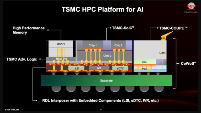
TSMC’s own localization efforts demonstrate how deeply materials are connected to manufacturing resilience. The company has worked with suppliers to localize electroplating additives used in advanced packaging, showing that resilience requires qualification at the chemical and process-material level—not merely construction of additional buildings.
The U.S. challenge will be replicating enough of this supplier density to operate fabs and packaging plants efficiently.
A semiconductor cluster cannot be built through capital expenditure alone. It requires experienced engineers, reliable utilities, rapid equipment servicing, qualified materials, spare-parts inventories and suppliers capable of responding to process excursions within hours rather than weeks.
Arizona may eventually become one of the world’s most important semiconductor manufacturing regions, but reproducing the operational efficiency accumulated in Taiwan over several decades will remain a long-term process.
A Two-Speed Semiconductor Industry
The strength of AI demand also masks growing divergence across semiconductor end markets.
TSMC said AI-related demand remained extremely robust, while consumer and price-sensitive markets continued to face pressure from rising component costs and macroeconomic uncertainty. Mature-node demand was described as relatively weak in several commodity segments, with stronger opportunities concentrated in areas such as power management and CMOS image sensors.
This suggests that the industry is becoming increasingly two-speed.
The first track includes AI accelerators, server CPUs, networking silicon, HBM, advanced packaging, optical interconnects and power infrastructure. These markets are attracting capital, engineering resources and strategic attention.
The second track includes consumer electronics, lower-end industrial products and price-sensitive devices. These markets may continue to grow, but their customers have less ability to absorb component inflation.
This divergence could create indirect constraints.
Capital equipment, engineering talent and supplier resources are finite. As more capacity is directed toward N2, A14, advanced packaging and AI-related products, other customers may experience less flexibility in pricing, lead times and prioritization.
TSMC has said it will continue investing in strategically important mature-node capacity, including facilities in Japan for applications such as image sensors and in Germany for automotive and industrial semiconductors. However, the allocation of incremental capital increasingly favors higher-value technologies and AI-related demand.
The AI boom therefore does not automatically lift every semiconductor category.
In some segments, it may increase costs without generating equivalent demand growth.

4月17日
Globalization Is Being Rearranged, Not Reversed
TSMC’s U.S. expansion does not mean that Taiwan is being replaced.
During the same earnings call, the company said it was constructing 13 leading-edge and advanced packaging fabs in Taiwan over the next several years. It is also expanding 3-nanometer capacity across Taiwan, Arizona and Japan while developing specialty capacity in Germany.
Taiwan will remain TSMC’s core technology-development and high-volume manufacturing base. Its semiconductor ecosystem continues to provide advantages in engineering density, supplier proximity, operating speed and production scale that cannot be replicated quickly.
What is changing is the architecture of globalization.
The old model pursued maximum efficiency by concentrating each stage of production in the most economically advantageous location. The emerging model balances three competing objectives:
Efficiency, resilience and political acceptability.
No region will maximize all three simultaneously.
Taiwan offers unmatched manufacturing concentration and operating efficiency. The United States provides proximity to major AI customers and alignment with national-security priorities. Japan offers strong materials, equipment and automotive ecosystems. Germany supports European industrial and automotive requirements.
The resulting network will be more resilient to certain disruptions, but it will also contain more duplication and structural cost.
This is not deglobalization in the traditional sense. It is controlled regionalization.

3月3日
What the Supply Chain Should Watch Next
Several indicators will determine how quickly this new structure develops.
The first is pricing.
The industry should watch whether reported 2027 increases are implemented across both leading-edge wafer fabrication and advanced packaging—and whether customers accept them without reducing orders.
The second is Arizona execution.
The key variables will not only be construction schedules. Labor productivity, equipment installation, utilities, supplier localization, yield ramp and cost control will determine whether Arizona can move from strategic symbolism to commercially scalable manufacturing.
The third is customer commitment.
Longer-term capacity agreements from Nvidia, AMD, Broadcom, Apple and major cloud providers would reduce TSMC’s investment risk. They would also deepen the divide between large customers capable of securing strategic capacity and smaller customers relying on remaining supply.
The fourth is packaging policy.
A domestic logic fab without sufficient HBM integration, substrates, test capacity and thermal infrastructure does not create a complete AI supply chain. Future U.S. industrial policy must increasingly focus on these supporting layers.
The fifth is total AI system cost.
Wafer prices are only one component. HBM, substrates, advanced packaging, networking, power equipment, cooling and data-center construction are all becoming more expensive. The market must eventually determine how much infrastructure inflation can be absorbed before customers delay deployments, optimize existing hardware more aggressively or shift toward lower-cost architectures.
The SemiVision Perspective
TSMC’s additional $100 billion commitment should not be interpreted merely as another capacity announcement.
It marks the transition of advanced semiconductor manufacturing from a globally optimized commercial activity into strategic infrastructure.
Once that transition occurs, several consequences follow.
Production becomes more geographically distributed. Governments play a larger role in investment decisions. Customers sign longer and deeper supply agreements. Manufacturing costs rise. Barriers to entry become higher. Advanced packaging and materials move closer to the strategic center of the industry.
Most importantly, resilience is no longer free.
7月4日
The semiconductor industry spent decades reducing costs through concentration, specialization and global scale. It is now being asked to preserve much of that technological performance while duplicating capacity across several regions.
That trade-off will define the next phase of the AI infrastructure supercycle.
The winners will not simply be the companies with the fastest GPUs or the smallest transistors. They will be the companies capable of securing and coordinating the entire system: leading-edge logic, HBM, packaging, substrates, power, cooling, materials and manufacturing capacity across multiple geographies.
TSMC’s Arizona expansion shows that the semiconductor industry has entered a more localized era.
It will also be a more expensive one.


PreviousNext