Why TLVR Will Not Kill MLCCs—and May Accelerate the Shift to VPD
Why TLVR Will Not Kill MLCCs—and May Accelerate the Shift to VPD
- Source: SemiVision
- Author: SEMIVISION
- Published: 2026-07-21T16:06:12+08:00
- URL: https://tspasemiconductor.substack.com/p/why-tlvr-will-not-kill-mlccsand-may Why TLVR Will Not Kill MLCCs—and May Accelerate the Shift to VPD


Why TLVR Will Not Kill MLCCs—and May Accelerate the Shift to VPD
Original Article By SemiVision Research [Reading time: 33 mins]

Jul 21, 2026
∙ Paid
Why TLVR Will Not Kill MLCCs—and May Accelerate the Shift to VPD
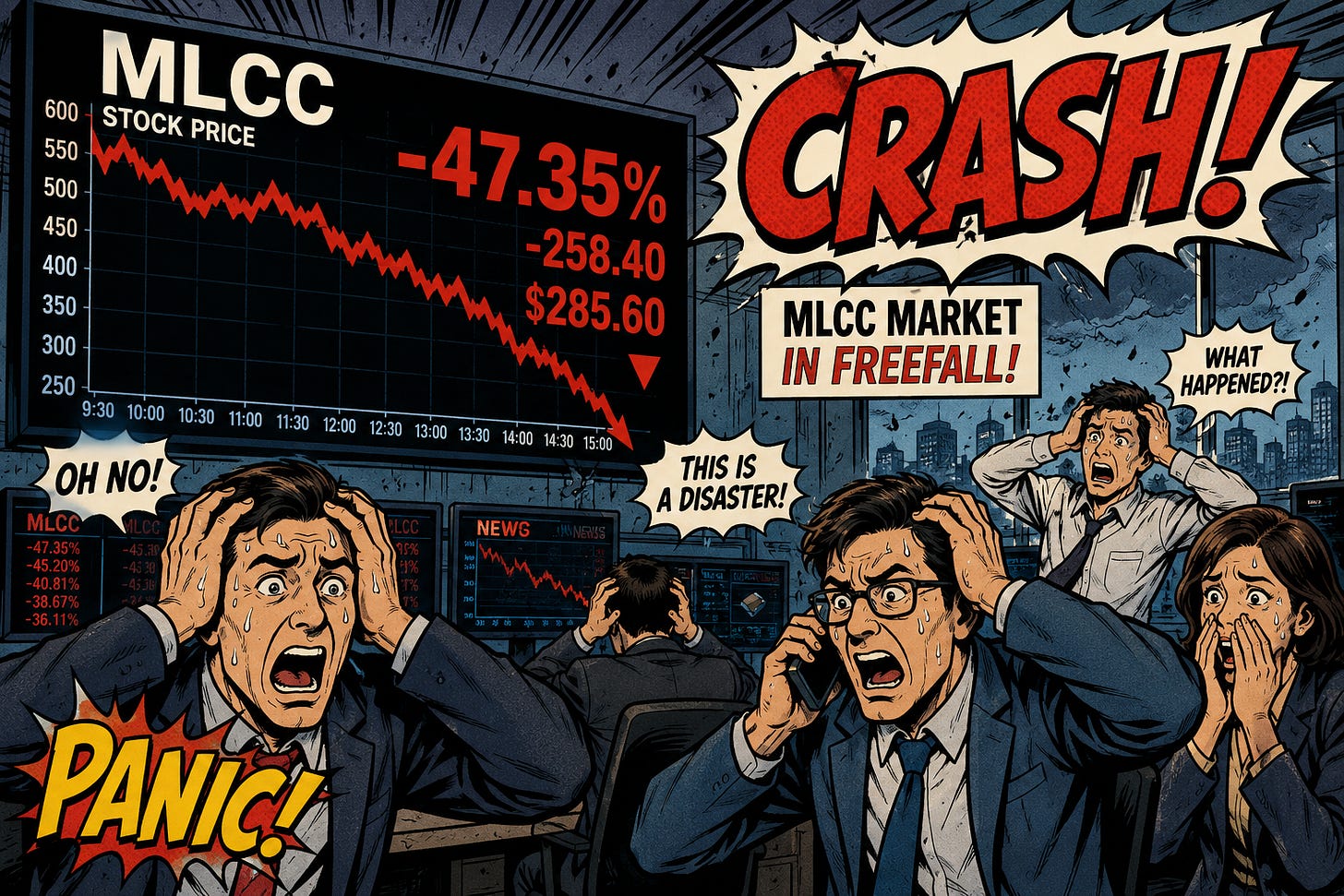
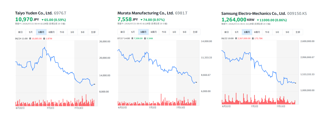
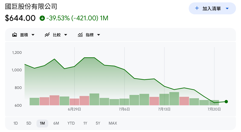
Passive-component stocks worldwide have recently undergone a sharp correction. Shares of Murata Manufacturing, Samsung Electro-Mechanics, Taiyo Yuden, Yageo, Walsin Technology, Holy Stone, and Chinese passive-component suppliers(Fenghua) all declined in tandem. The market quickly attributed the selloff to an argument that appears plausible but is in fact overly simplistic: as NVIDIA AI GPUs adopt TLVR and improve power-supply transient response, systems can eliminate large numbers of MLCCs, reducing demand for high-end multilayer ceramic capacitors in AI servers.
YAGEO Group

fhcomp.com
This argument focuses on a single component within the power-delivery architecture while overlooking the simultaneous changes in AI-chip power, transient current, the number of power rails, package size, HBM count, and the location of power conversion. TLVR may indeed reduce part of the board-level output-capacitance requirement in certain designs, but that is not equivalent to eliminating decoupling capacitors, nor does it imply that total MLCC content across an AI system must decline. On the contrary, as AI GPUs move from hundreds of watts to several kilowatts while core operating voltages remain in the low-voltage range of roughly 0.6-1.0 V, current will rapidly rise into the kiloampere and even multi-kiloampere range. Parasitic resistance, parasitic inductance, voltage droop, load transients, and anti-resonance across the power path will become more severe, forcing capacitance to be distributed across more locations, more voltage levels, and more package structures.
The real question, therefore, is not whether TLVR will replace MLCCs, but rather this:
The AI power-delivery network is shifting from centralized board-level decoupling toward a distributed decoupling architecture shared across the board, package underside, interposer, voltage regulators, and the backside of the chip.

7月7日
The following analysis rebuilds a more complete framework by examining the relationships among chip core voltage, AI workload characteristics, TLVR, eDTC, IVR, CoWoS-L, 800 V HVDC, and VPD.

A Stock-Price Collapse Does Not Mean the MLCC Demand Structure Has Collapsed
The first step is to separate stock-price performance from technical demand.
The steep declines in passive-component stocks shown in the market do no more than demonstrate a change in growth expectations, valuation, or capital allocation for the passive-component industry. They do not directly prove that actual MLCC consumption has collapsed because of TLVR. Passive-component companies are simultaneously exposed to smartphones, automobiles, industrial equipment, consumer electronics, foreign exchange, inventories, utilization rates, product mix, raw-material costs, and market valuation. Even if AI servers represent an important incremental market, synchronized corrections across these companies cannot be attributed to a single power topology.

Murata, Taiyo Yuden, Samsung Electro-Mechanics, Yageo, and Walsin Technology also have materially different product portfolios. Their exposure to general-purpose MLCCs, automotive MLCCs, high-capacitance MLCCs, low-ESL MLCCs, polymer capacitors, tantalum capacitors, inductors, and resistors varies significantly. Interpreting all of their share-price declines through the single lens of ‘TLVR reduces MLCCs’ is not rigorous industry analysis.
Two Products, Two Audiences, One Research Platform

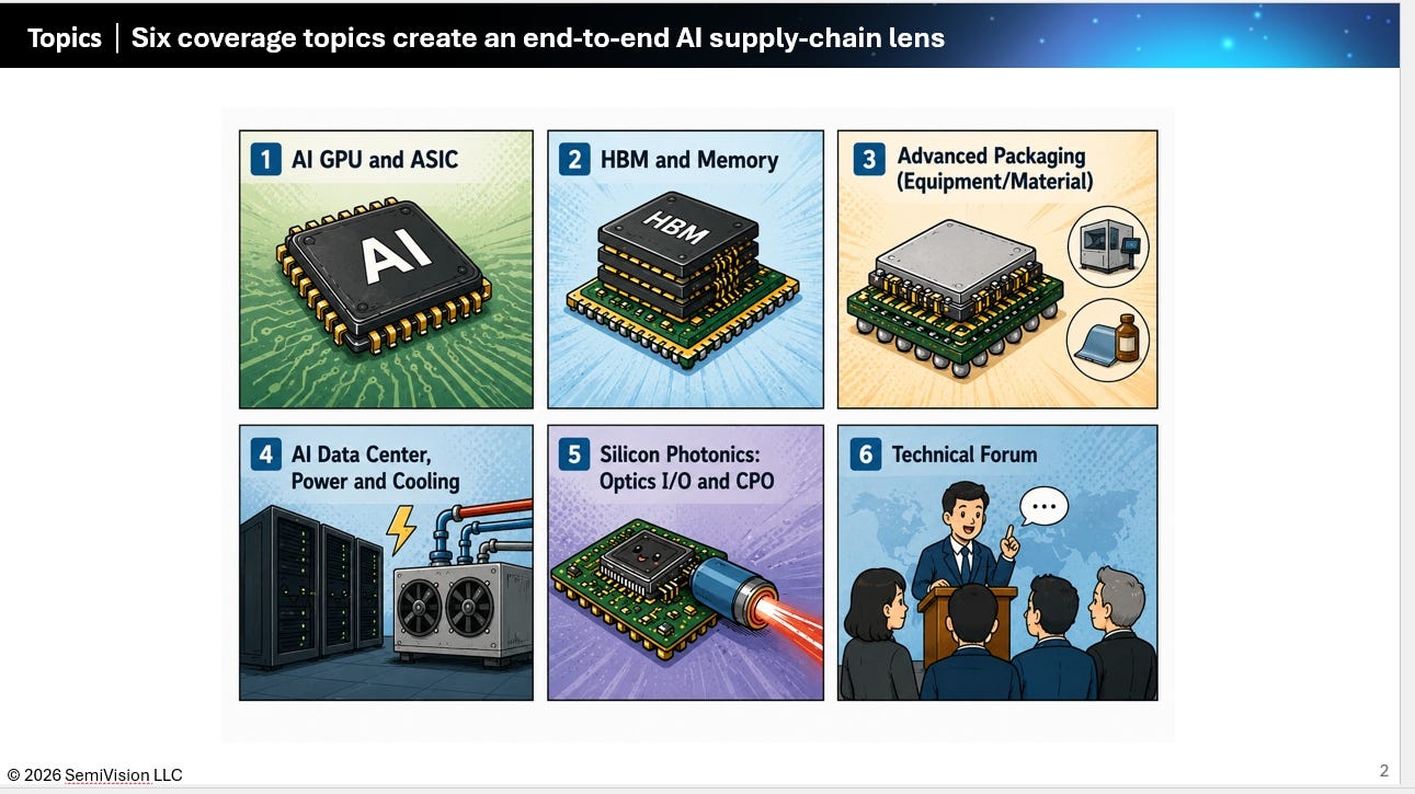
The SemiVision Monthly Reportprovides in-depth analysis of the semiconductor industry and key technologies, along with timely updates on the global supply chain. To deliver comprehensive and forward-looking market insights, our coverage is tailored acrosssix core sectors.For more details or subscription information, please feel free to contact us.

Contact us for more information:
jett@semivisiontw.com / eddyt@semivsiontw.com
Below we will share:
Why Is TLVR Better Viewed as a Transitional Solution?
What Exactly Is TLVR, and Why Does the Market Believe It Will Reduce MLCC Content?
eDTC and MLCC Serve Different Functions; They Are Not Simple One-for-One Substitutes
Due to space limitations in this issue,SemiVisionwill continue to monitor and provide in-depth analysis of the latest technical advancements and industry trends in MLCCs in upcoming features.
A more precise interpretation is that the market has begun to worry that changes in board-level power architecture for AI servers could reallocate some traditional MLCC placements, raising questions about the long-term passive-component value per system. Yet a change in placement does not mean total demand disappears. Partial compression of board-level MLCC content may occur alongside rising decoupling requirements at the package, high-frequency, input, and multi-rail levels.
Accordingly, analysis cannot focus only on the number of MLCCs at one location. It must evaluate the entire Power Delivery Network, or PDN: total capacitance, frequency coverage, the number of voltage domains, reliability requirements, and capacitor value per watt.
The Fundamental Contradiction in AI-Chip Power Delivery: Power Keeps Rising, but Core Voltage Cannot Rise with It
The difficulty of powering an AI GPU begins with a very direct physical relationship:
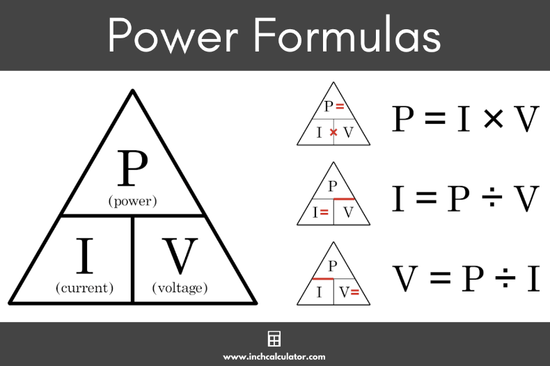
When chip power increases while core voltage remains at roughly 0.6-1.0 V, the required current rises dramatically.
Assume that the core-related power of a GPU is 1,200 W and the supply voltage is 0.7 V. Under ideal conditions, the current is approximately:
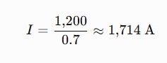
If the combined power of compute dies and related power rails within a future package approaches 3,000 W, theoretical current at 0.65 V could exceed 4,600 A. A real product would not place all power on a single rail, but this calculation captures the central problem of AI-chip power delivery: even at a fraction of a volt, current can reach several thousand amperes.
Such enormous current creates substantial power loss even through extremely small resistance:

Even if the equivalent resistance of the power path is only 0.1 mΩ, a current of 2,000 A still produces:
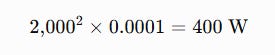
This is why the core challenge of future power architecture is not merely to improve conversion efficiency, but to shorten the low-voltage, high-current path. Delivering high current laterally from the edge of a motherboard into a large GPU package creates copper loss, IR drop, parasitic inductance, and severe space constraints.
In its advanced-packaging power-technology materials, TSMC likewise describes a progression from conventional board-level multiphase DC/DC conversion toward a higher intermediate input voltage, followed by in-package IVR conversion down to approximately 0.7-1.0 V. Its public technology roadmap indicates that future CoWoS-R and CoWoS-L platforms will incorporate DTC, eDTC, and IVR, and explicitly points toward Vertical Power Delivery IVR.

Therefore, 800 V HVDC, TLVR, IVR, eDTC, and VPD are not mutually substitutable technologies. They are solutions operating at different physical scales and voltage levels.
800 V HVDC Solves the Data-Center and Rack Problem; It Does Not Deliver 800 V Directly to the GPU Core
A common source of confusion in market discussions is this: if data centers are moving toward 800 V HVDC, does that mean GPUs will also be powered directly at 800 V?
The answer is no.
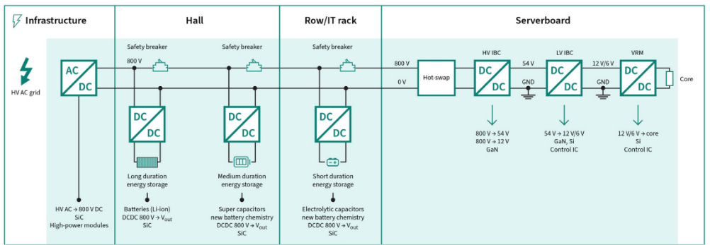
800 V HVDC is a data-center- and rack-level power-distribution architecture. Its primary objective is to raise transmission voltage and reduce current at a given power level, thereby reducing copper loss, cable volume, and the footprint of power-distribution equipment. NVIDIA’s published architecture shows that after 800 V DC enters the rack, it still passes through DC/DC conversion to 54 V, 12 V, or another intermediate bus voltage before being converted to the approximately 0.7-1.0 V required by the GPU core.

NVIDIA has further disclosed that the Kyber-generation concept distributes 800 V close to the compute nodes, then uses a high-ratio converter to step the voltage down to 12 V before the final low-voltage stage that powers the GPU. In other words, 800 V HVDC addresses long-distance, high-power transmission, whereas VPD addresses low-voltage, high-current delivery over the final few centimeters or even millimeters.
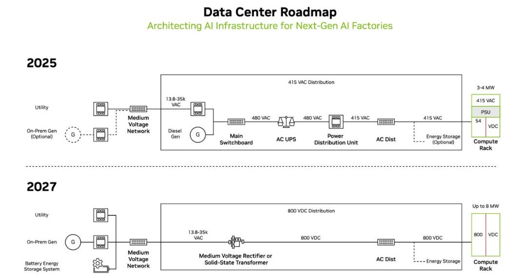
The two approaches actually follow the same principle:
Raise voltage to reduce current over long transmission distances; then, near the chip, place the converter as close to the load as possible to shorten the low-voltage, high-current path.
An 800 V architecture therefore does not eliminate decoupling requirements. On the contrary, as the system incorporates more stages of high-frequency DC/DC conversion—from 800 V to 54 V, 12 V, 1.8 V, and finally 0.7 V—each converter stage requires corresponding filtering, energy-storage, and voltage-stabilization components at both its input and output.
Capacitor demand will therefore become increasingly stratified:
The 800 V bus requires high-voltage film capacitors and bulk energy-storage devices; the 54 V and 12 V stages require polymer, aluminum electrolytic, tantalum, or high-capacitance MLCC solutions; the 1-2 V region near the GPU package requires low-ESL, low-ESR, high-frequency MLCCs and silicon capacitors; and the chip and interposer require eDTC, MIM, and on-die decoupling capacitors.
The adoption of TLVR at one layer therefore cannot be used to infer a decline in capacitor demand across the entire power-delivery chain.

6月27日
AI Workloads Are Not Steady Loads, but Highly Synchronized Transient-Power Loads
Traditional CPU and general server workloads usually exhibit some degree of asynchrony, allowing load changes across different cores and nodes to partially offset one another. Large-scale AI training and inference systems, however, often execute matrix operations, communications, memory access, and collective operations in synchronization. Tens, hundreds, or even thousands of GPUs may transition from low to high load at nearly the same time.
NVIDIA’s description of the GB300 NVL72 notes that GPU power fluctuations in AI training workloads are highly synchronized, causing the cluster to amplify the power variation of each individual GPU. This is also why NVIDIA has introduced power smoothing at the rack level.
For an individual GPU, an instantaneous load transition produces:

This equation shows that voltage deviation has three components:
First, the instantaneous voltage drop caused by ESR; second, the spike generated by ESL and the rate of current change; and third, the voltage change caused by the capacitor supplying charge before the control loop can respond.
TLVR primarily improves the regulator’s response speed to load changes and coordinates current across multiple phases, shortening the interval before the inductors and controller take over the load. Yet even the fastest controller cannot eliminate parasitic inductance in the power-delivery path. Between the moment the load begins drawing current and the moment the regulator increases output current, local capacitors must still supply energy.
In other words, TLVR can shorten the period during which capacitors must independently support the load, but it cannot reduce that period to zero. Nor can it eliminate the parasitic parameters of the package, solder balls, substrate, motherboard, and power planes.
TLVR changes the optimal capacitance design point; it does not eliminate capacitance itself.
What Exactly Is TLVR, and Why Does the Market Believe It Will Reduce MLCC Content?
TLVR generally refers to a Trans-Inductor Voltage Regulator. Its core concept is to add a coupled or transformer-like auxiliary magnetic path to the inductors of a multiphase step-down converter, allowing the currents of multiple phases to respond collectively and more rapidly to load changes.
In a conventional multiphase buck architecture, the current slew rate of each phase is constrained by the input-output voltage differential and the inductance value:
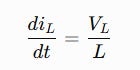
To reduce steady-state current ripple, designers tend to use larger inductors. However, the larger the inductance, the more slowly current can rise during a sudden load increase. This creates the classic tradeoff between transient response and steady-state ripple.

Through magnetic coupling, TLVR enables multiple phase inductors to support the output more effectively during a sudden load transition, reducing effective transient inductance while maintaining reasonable current ripple in steady-state operation. Because the regulator can replenish current faster, it can theoretically reduce part of the bulk output capacitance required within the same allowable voltage window.
This is the origin of the claim that ‘TLVR reduces MLCCs,’ and the claim is not entirely wrong.
The error lies in extending ‘required capacitance may decline at a specific output node’ into ‘total MLCC demand across the AI system will decline.’
What TLVR can mainly displace is part of the board-level output capacitance determined by low- to mid-frequency transient requirements—especially the large capacitor banks historically used while waiting for the VRM control loop to respond. High-frequency load spikes, localized current changes inside the chip, package parasitic inductance, power-plane anti-resonance, and isolation across multiple rails still require decoupling capacitors at different physical locations.
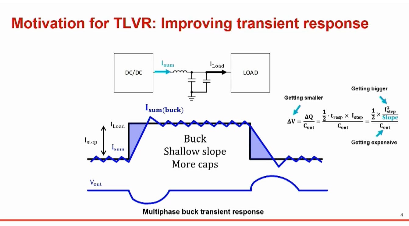
TLVR also carries its own costs. It requires additional magnetic components, coupled windings, more complex layout and control, and may introduce core loss, winding loss, leakage inductance, interphase imbalance, EMI, thermal-density, and manufacturing-tolerance challenges. As GPU packages become larger and current rises further, board-level TLVR still cannot change the fact that low-voltage, high-current power must travel laterally across the motherboard and package substrate.
TLVR is therefore an important improvement over conventional multiphase VRMs, but it is not the ultimate power-delivery architecture.
Why Is TLVR Better Viewed as a Transitional Solution?
Calling TLVR transitional does not mean it will disappear soon. It may remain in use across multiple product generations and may even coexist with VPD. ‘Transitional’ means that it is still built on the basic logic of voltage conversion at the board or package perimeter and does not fundamentally solve the transmission distance of the final low-voltage, high-current segment.
A conventional lateral power-delivery architecture can be summarized as follows:
Motherboard power modules are positioned around the GPU package. Current flows from the VRM through motherboard copper layers, solder balls, and the package substrate, entering at the package edge and traveling toward the central die.
When GPU packages were smaller and consumed only a few hundred watts, this approach could be supported by increasing copper thickness, power-plane count, phase count, and capacitor count. As CoWoS packages expand and HBM stack counts rise, however, the area around the package is increasingly occupied by HBM, I/O, optical interfaces, connectors, and cooling structures, forcing the power path to become longer and more complex.
TSMC’s published CoWoS roadmap shows the interposer expanding from approximately one reticle in early generations to 3.3, 5.5, and eventually more than eight reticles, while HBM count increases from four stacks to more than twelve HBM4 stacks. As package size and compute density rise, eDTC, DTC IPD, and IVR have been incorporated into the CoWoS-R and CoWoS-L roadmaps.

Source: Navitas
The larger the package, the longer the lateral distance from the edge to the center. The higher the current, the more severe the IR drop and Ldi/dt effects across the power network. Even if TLVR accelerates the board-level current ramp, it cannot eliminate parasitic impedance within the motherboard and package.
The real solution must be to:
Move converters, inductors, and capacitors directly beneath the GPU or inside the package, allowing current to enter the compute die vertically instead of traveling laterally across the entire substrate from the package edge.
That is the essence of VPD.

eDTC and MLCC Serve Different Functions; They Are Not Simple One-for-One Substitutes
eDTC stands for embedded Deep Trench Capacitor. It forms high-aspect-ratio trenches in silicon, using three-dimensional surface area to increase capacitance per unit area, and integrates the capacitor directly into a silicon interposer, local silicon interconnect, or another package structure.
TSMC has already integrated eDTC into volume-produced CoWoS-S, while CoWoS-L can use LSI and eDTC to improve signal and power integrity. TSMC’s annual report states that silicon interposers in CoWoS-S have incorporated eDTC for years, and that CoWoS-L scales HPC products by combining an RDL interposer, LSI, and eDTC.

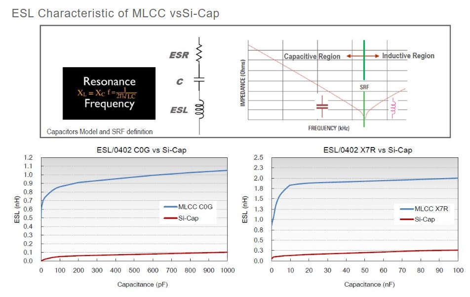
The primary advantage of eDTC is not simply large capacitance. It is the extremely short distance to the chip and the correspondingly short interconnect path, which gives it substantially lower ESL than surface-mounted MLCCs on the motherboard. For high-frequency current spikes, proximity often matters more than nominal capacitance.
A 100 µF capacitor on the motherboard may present higher effective high-frequency impedance than a smaller but ultra-low-ESL capacitor embedded in the interposer once long traces, vias, solder balls, and the package substrate are included. eDTC is therefore well suited to high-frequency decoupling and local voltage stabilization.
However, eDTC cannot cover every frequency range and energy requirement.
High-frequency transients require nearby low-ESL capacitors; mid-frequency load changes require package- and board-level MLCCs; and lower-frequency or longer-duration power fluctuations require polymer, tantalum, aluminum capacitors, or rack-level energy storage.
A complete PDN is not implemented with a single capacitor type. It is constructed from components with different impedance and frequency characteristics. The objective is to keep PDN impedance below the target impedance across a broad frequency range:
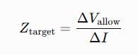
If the GPU core permits only 20 mV of voltage variation while instantaneous current changes by 1,000 A, the target impedance is only:
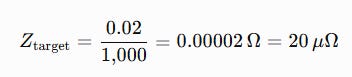
Twenty micro-ohms is an extremely low impedance. eDTC, TLVR, or MLCC alone cannot maintain it across the full frequency range. The solution requires on-die capacitors, eDTC, package-level MLCCs, board-level MLCCs, polymer capacitors, power planes, and active control working together.
The growth of eDTC is therefore not evidence that MLCCs are disappearing. It is evidence that the PDN is evolving from a single-layer board-decoupling architecture into a multilayer decoupling architecture.
One Point Requires Correction: eDTC Does Not Address ‘Excessive Voltage’; It Suppresses Power-Delivery Impedance and Voltage Fluctuation
The original argument stated that ‘excessive voltage causes ripple in the device, so eDTC is needed to improve stability.’ This statement requires some refinement.
Ripple is not caused simply by an excessively high input voltage. It primarily originates from the periodic switching of switched-mode power supplies, inductor-current ripple, changes in load current, and the ESR, ESL, and resonance of the power-delivery network. For a GPU core, the real danger is any core-voltage excursion beyond specification, including overvoltage, undervoltage, periodic ripple, and transient spikes.
The role of eDTC is to reduce PDN impedance across a specific frequency range, provide short-duration charge to the chip, and mitigate Ldi/dt voltage drop and local droop along the power path. It is not itself a voltage regulator and does not determine the output voltage.
IVR is the active element responsible for voltage conversion and regulation; eDTC, MLCCs, and other decoupling capacitors are passive elements for energy storage and filtering.
Their functions can be simplified as follows:
IVR determines the voltage level, while eDTC and MLCCs help keep that voltage stable during rapid load changes.
eDTC and IVR therefore cannot be treated as functionally equivalent, much less as substitutes for one another. As IVR switching frequency increases and the regulator moves closer to the chip, properly designed input and output decoupling becomes even more important for controlling switching ripple and current loops.
IVR Provides Active Step-Down Conversion, While eDTC Provides Passive Energy Storage; Together They Form In-Package Power Delivery
IVR, or Integrated Voltage Regulator, integrates part or all of the voltage regulator near the chip or within the package. A conventional board-level VRM might convert directly from 12 V to 0.7 V. A future architecture may first convert 48 V or 12 V to an intermediate voltage of 1.8-6 V, then use an in-package IVR for the final step-down stage.
This design offers several important advantages.
First, raising the voltage delivered to the package reduces transmission current. If 1,000 W is supplied to the package, transmission at 0.7 V requires approximately 1,429 A; at 1.8 V, approximately 556 A; and at 6 V, only about 167 A. A nearby IVR can then convert the voltage to 0.7 V, significantly reducing copper loss in the motherboard and package substrate.
Second, because the IVR is closer to the chip, its control loop can respond more quickly to local load changes and reduce power-supply interference among different compute blocks.
Third, different chiplets can operate at different voltages. A future large AI package may simultaneously contain GPU compute dies, I/O dies, HBM base dies, SerDes, NVLink, CPO electronic ICs, PHYs, and security-control chips. The optimal operating voltage differs for each type of component. In-package IVR enables finer-grained power domains and dynamic voltage adjustment.
TSMC’s public materials indicate that next-generation CoWoS platforms can combine eDTC, CoWoS-S technology, and an RDL interposer, then further integrate a chip-scale IVR containing inductors and capacitors, with development progressing toward Vertical Power Delivery IVR.
This architecture does not imply lower capacitor demand. IVR itself requires:
Input decoupling capacitors, output filter capacitors, switching-node suppression, local load decoupling, isolation among different voltage domains, and impedance control between the package and motherboard.
Moving power conversion into the package merely redistributes capacitor locations and specifications.
Why Do Multiple Power Domains in CoWoS-L Increase Decoupling Complexity?
It is important to distinguish precisely between the number of package layers and the number of power rails. Each additional RDL layer in CoWoS does not automatically correspond to an independent voltage. What actually increases decoupling demand is the addition of more dies, more functional blocks, and more independent power domains.
A large AI package typically includes:
Compute-core power, SRAM or cache power, I/O power, SerDes power, HBM core power, HBM I/O power, PLL and clock power, analog power, PHY power, controller power, and security and management power.
Each rail has a different operating voltage, load profile, noise sensitivity, and allowable ripple. A high-current core rail may require an extremely low target impedance; PLLs and high-speed SerDes draw less current but are more noise-sensitive; HBM I/O must simultaneously satisfy high-speed signal-integrity and power-integrity requirements.
As the package becomes larger and includes more HBM stacks and dies, the number of power domains generally increases. Each domain requires its own decoupling network. Some capacitance can be shared, but much of the high-frequency decoupling must remain close to its respective load.
Future MLCC demand in AI packages therefore cannot be assessed merely by the total microfarads required for a single core rail. The analysis must consider:
The number of power rails, current on each rail, noise tolerance, degree of load synchronization, package location, capacitor derating, thermal environment, and failure requirements.
Even if TLVR reduces some bulk MLCC content on the core output rail, that reduction may be offset by demand from additional I/O, HBM, SerDes, and package-input rails.
The Shift from Lateral Power Delivery to VPD Is an Inevitable Evolution of AI Packaging
The largest problem with conventional power delivery is that low-voltage, high-current power must enter from the side of the chip. As package dimensions increase, current must travel farther laterally to reach the central region. This creates three problems:

Source: VLSI 2026 TSMC
First, resistive loss increases. Longer conductors have higher resistance, and higher current produces more severe I²R loss.
Second, parasitic inductance increases. During rapid load switching, even tens to hundreds of picohenries of parasitic inductance can produce significant voltage excursions.
Third, power and signals compete for routing resources. A CoWoS package must support large numbers of HBM and high-speed die-to-die signals while simultaneously delivering several thousand amperes. If all signals and power enter from the package edge, routing congestion deteriorates rapidly.
The concept of VPD is to place the power converter or power-delivery structure directly beneath the chip so that current enters the chip vertically. Possible implementations include:
Placing the VRM on the backside of the package; stacking an IVR die beneath the compute die; delivering current through TSVs or a backside metal network; integrating magnetic components and capacitors on the package underside; or combining a power IC, inductor, and deep-trench capacitor into a standalone power chiplet.
Research shows that a 3D chip-on-VRM configuration, in which the VRM is placed beneath the chip, can effectively reduce power-supply noise at high-current-density hotspots because the distance between converter and load is minimized.
NVIDIA has also demonstrated a 1,500 A, 48 V-to-1 V switching bus converter aimed at single-stage VPD for next-generation ultra-high-power GPUs. Such designs show that NVIDIA is already exploring a transition from board-level multiphase power toward vertical delivery located closer to the GPU.
What VPD fundamentally solves is not that the power converter responds too slowly, but that low-voltage, high-current power should no longer travel over a long lateral distance.
This is the fundamental issue TLVR cannot fully address.
VPD Will Not Eliminate MLCCs; It May Instead Increase Capacitor Value per Watt
The market may extend the argument further: if VPD places IVR, inductors, and eDTC beneath the chip, MLCCs will ultimately still be replaced.
This conclusion is equally oversimplified.
VPD may indeed reduce the large number of standard MLCCs traditionally placed on the motherboard around the GPU package, but it simultaneously creates new capacitor requirements:
First, the VPD input still requires decoupling. If the package input is 12 V, 48 V, or another higher intermediate voltage, low-impedance input capacitors must be placed around the power module to prevent switching current from feeding directly back into the motherboard power network.
Second, the IVR output still requires low-ESL capacitance. Even when the voltage regulator sits directly beneath the chip, it cannot respond instantaneously to nanosecond-scale load changes. On-die capacitors and eDTC closest to the load handle the highest frequencies, while package-level MLCCs cover the next frequency band.
Third, multiple vertical power modules may serve different regions. As GPU area increases, a single centralized IVR may be replaced by several distributed power cells, each requiring local decoupling and input filtering.
Fourth, the package thermal environment becomes more severe. Capacitors near the GPU and IVR must offer better temperature stability, lower DC-bias degradation, and higher mechanical reliability. Their value per component may be substantially higher than that of general consumer-grade MLCCs.
Fifth, VPD increases the importance of low-ESL package formats. The terminal electrodes and mounting orientation of conventional two-terminal MLCCs constrain ESL. Future designs may increasingly use reverse-geometry MLCCs, three-terminal capacitors, silicon capacitors, LICC, or embedded capacitors to shorten the current loop.
VPD therefore does not produce a capacitor-free architecture. It drives capacitors toward higher frequency, deeper package integration, greater customization, and higher unit value.

Source: AMD
MLCC Unit Count May Decline Locally, but Total MLCC Value Does Not Necessarily Decline
Passive-component analysis cannot rely solely on unit count. It must also evaluate capacitance, case size, voltage, temperature, dielectric material, ESR, ESL, reliability, and qualification requirements.
Moreover, passive-component value in an AI server must be calculated at the system level, not from a single GPU alone:
Power per GPU increases; GPU count per compute tray rises; the number of GPUs and switch chips per rack increases; NIC, DPU, NVSwitch, CPO, and HBM content expands; the number of 54 V, 12 V, and low-voltage-rail power modules rises; and both BBUs and power shelves require substantial capacitance.
Even if one category of board-level MLCC declines per GPU, passive-component value across the entire rack may still grow as power density and system complexity increase.
The correct industry assessment should therefore distinguish among three layers:
Whether general consumer MLCCs benefit; whether high-capacitance server MLCCs benefit; and whether package-level low-ESL, high-reliability capacitors benefit.
The strongest growth may not accrue to the entire MLCC market, but to high-end suppliers qualified for AI power modules, locations near GPU packages, switches, BBUs, and high-voltage DC/DC converters.
MLCCs, eDTC, and SiCap Are Complementary, Not Simple Substitutes
Different capacitor technologies will divide the workload within future AI PDNs.
On-die decoupling capacitors sit closest to the transistors and primarily serve the highest-frequency, shortest-duration current demand, but silicon area is expensive and available capacitance is limited.
eDTC and SiCap provide extremely low ESL, strong high-frequency performance, and efficient use of area. They are suitable for interposers, LSI, or in-package integration, but remain constrained by cost, process integration, and capacitance range.
MLCCs benefit from a mature supply chain and a broad range of capacitance and voltage ratings. They are suitable for package surfaces, substrate undersides, motherboards, and power modules, particularly for mid- to high-frequency decoupling.
Polymer tantalum and polymer aluminum capacitors offer higher capacitance and more stable DC-bias characteristics, making them suitable for mid- to low-frequency response and high-current outputs.
Film and electrolytic capacitors serve higher-voltage applications and longer-duration energy storage.
A well-designed PDN does not allow one capacitor technology to completely replace all others. It combines the impedance characteristics of different components to flatten the overall impedance profile and avoid anti-resonance peaks.
Simply increasing MLCC count may create anti-resonance through the parasitic parameters of components with different capacitance values. Reducing MLCC content too aggressively, however, may push mid-frequency impedance above the target. Future design will focus on joint optimization through simulation, measurement, and active control rather than maximizing or minimizing capacitor count in isolation.

From Blackwell and Rubin to Rubin Ultra, Power Delivery Will Only Become More Difficult
NVIDIA’s development direction has shifted from optimizing a single GPU to treating the entire rack as the unit of computing. The Vera Rubin platform likewise emphasizes extreme co-design across GPUs, CPUs, networking, power, and cooling.
As systems move beyond NVL72 toward higher GPU density, the challenge is not simply higher TDP per chip. It also includes:
More GPUs, more HBM stacks, more NVLink switch chips, more CPO and optoelectronic components, greater synchronization of compute workloads, and rack power rising into the hundreds of kilowatts and eventually the megawatt range.

6月11日
NVIDIA has identified 800 V DC as a critical foundation for the next generation of AI factories and is planning the Kyber architecture to support denser Rubin Ultra systems.
However, raising rack input to 800 V solves only upstream distribution efficiency; the GPU core still operates at low voltage. As the industry moves further toward 800 V HVDC, the final high-step-down-ratio, high-current-density DC/DC stage becomes more—not less—important.
Stepping down from 800 V to 0.7 V represents a total conversion ratio of more than 1,100:1, which cannot be achieved efficiently with a single conventional buck converter. The system must use staged conversion:
800 V to an intermediate bus, then to 48 V or 12 V, then to several volts, and finally through an IVR to the core voltage.
Every stage involves energy storage and filtering. Architectural innovation may reduce the number of conversion stages, but the power density, switching frequency, and capacitor stress at each remaining stage will increase.
The trend in AI power delivery is therefore not the disappearance of passive components, but the joint migration of passive components and active power semiconductors into the package.
An example of an HV data center architecture by Infineon
Why Will Future Systems Require More ‘Effective Capacitance’?
Effective capacitance differs from the nominal capacitance printed on a component. MLCCs are affected by DC bias, temperature, frequency, aging, and tolerance. An MLCC rated at 100 µF may provide effective capacitance far below its nominal value under actual operating voltage and elevated temperature.
The operating environment for MLCCs around an AI GPU is particularly demanding:
High DC bias, high temperature, mechanical bending, high-frequency ripple, high di/dt, and sustained full-load operation.
To achieve a required effective capacitance, designers therefore usually need to install nominal capacitance above the theoretical value. Future power rails will have narrower allowable voltage windows, larger load currents, and lower target impedance, further increasing effective decoupling requirements.
TLVR can reduce demand in certain frequency bands, but the higher ΔI of AI chips may simultaneously push requirements upward. Final capacitance demand reflects the interaction of two opposing forces:
Improved power topology reduces the requirement; higher chip power and larger load transients increase it.
If the second force grows faster than the first, total MLCC demand can still increase.
This is the point most easily overlooked by the market. The improvement delivered by a next-generation power architecture for the same chip cannot be used directly to estimate the component count of a next-generation chip relative to its predecessor, because the chip’s power, area, current, and load characteristics have also changed.
The Real Drivers of Future MLCC Demand Growth
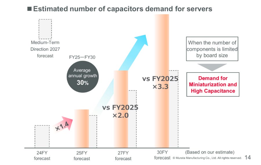
Future MLCC demand in AI systems will not be driven primarily by the consumer-electronics model of simply adding more units. It will be driven by the following structural factors.
Source: murata
First, higher power density. Each GPU and each rack must process more power, increasing the current ratings required for both input and output decoupling.
Second, more power domains. GPUs, HBM, SerDes, CPUs, DPUs, CPO, and switch chips each require different power rails.
Third, more high-speed signaling. High-speed SerDes, NVLink, and optoelectronic components are more sensitive to supply noise and require more precise local decoupling.
Fourth, distributed conversion. Centralized board-level VRMs are gradually giving way to multiple point-of-load IVRs or power modules, each of which requires input and output capacitance.
Fifth, higher reliability requirements. AI servers operate under sustained high load, and their components must withstand high temperature, thermal cycling, and high ripple current.
Sixth, 800 V DC drives more intermediate-bus conversion. Different levels of the power chain require different capacitor technologies, increasing total power-component value.
Seventh, packages continue to expand. The larger the package, the more difficult it becomes for one centralized capacitor bank to serve every local load, making distributed decoupling necessary.
The true long-term risk to MLCCs is therefore not that AI systems no longer need capacitors. It is that low-end standard products may be reassigned as high-end MLCCs, SiCap, eDTC, and polymer capacitors divide the application space. A supplier’s ability to enter high-end products will matter more than whether the overall MLCC market grows.

6月15日
Which MLCC Categories May Be Compressed, and Which May Benefit?
The category most likely to be compressed by TLVR is the medium- to high-capacitance MLCC bank placed at the board-level core-power output to compensate for the relatively slow transient response of a conventional VRM. On motherboards with conservative design margins and excessive capacitance redundancy, TLVR and more advanced control algorithms can indeed optimize the bill of materials.
The following product categories, however, may benefit:
Low-ESL and reverse-geometry MLCCs, because limited space around the package demands lower parasitic inductance.
High-capacitance, high-temperature-stability MLCCs, because the thermal environment near GPUs and power modules is severe.
High-voltage MLCCs, because the number of 12 V, 48 V, and other intermediate-bus power modules is increasing.
Three-terminal and low-impedance filtering components, because high-speed I/O and analog rails face tighter noise requirements.
Package-level and embedded capacitors, because VPD and IVR move power components into the package.
High-reliability industrial- and automotive-grade products, because AI servers require longer service life and lower failure rates.
Any claim that ‘MLCC demand is declining’ must therefore be qualified: What capacitance? What case size? What voltage? At what location? Serving which power rail?
Without these conditions, a discussion based only on unit count has little analytical value.
The Real Supply-Chain Divide: General Passive-Component Manufacturers vs. AI Power-Platform Suppliers
Future competition among passive-component suppliers will no longer be limited to ceramic-powder technology and sintering capacity. It will depend on whether suppliers can participate in the co-design of AI-system PDNs.
High-end suppliers will need capabilities that include:
Effective-capacitance data under DC bias, complete ESR and ESL models, GHz-range impedance models, thermomechanical reliability, joint motherboard-and-package simulation, low-inductance terminal-electrode design, customized form factors, and co-design capabilities with VRM, IVR, inductor, and packaging suppliers.
This means that the AI MLCC market will not be distributed evenly across all suppliers. Even if total content value grows, companies unable to provide accurate models, low-ESL designs, and high-reliability qualifications may still face pricing pressure.
Japanese suppliers have advantages in materials, miniaturization, and high reliability; Korean suppliers have stronger integration with memory, substrates, and large electronic systems; and Taiwanese suppliers may enter through the AI-server ODM, power-module, and PCB supply chains.
The most important question is not whether a company claims AI-related MLCC revenue, but whether:
Its products are designed into GPU baseboards, power shelves, NVSwitch systems, CPO modules, BBUs, or the package perimeter; whether they are standard products or low-ESL, high-capacitance products; whether they have passed high-temperature and high-ripple-current qualification; whether the supplier provides power-integrity models; and whether it participates in co-development of next-generation VPD and IVR modules.
3月26日
From an Investment Perspective, the Market’s Real Error Is Its Time Horizon
The market often reprices an entire industry on the basis of a single technology event. It sees TLVR reduce some capacitance and immediately concludes that MLCCs are entering long-term decline; it sees eDTC introduced into CoWoS and concludes that ceramic capacitors will be replaced by silicon capacitors.
Power-architecture evolution, however, does not occur instantaneously. Multiple product generations coexist.
A large installed base of AI servers still uses board-level multiphase VRMs and large numbers of MLCCs. TLVR penetration will rise gradually. In-package eDTC is already in volume production, but its capacitance, cost, and placement remain constrained. IVR and VPD will be introduced progressively as power density increases.
For a considerable period, the market may simultaneously include:
Conventional board-level VRMs, TLVR, in-package eDTC, local IVR, backside VRMs, and multiple forms of VPD.
Different GPUs, ASICs, CPUs, and CSP-designed chips will not use the same architecture. Cost-sensitive inference chips may retain board-level power delivery; the highest-end training GPUs may adopt VPD first; and networking ASICs and CPO systems may use another form of local power delivery.
The technology path of the highest-end product therefore cannot be applied directly to the entire MLCC market, nor should the market assume that every board-level capacitor will disappear within a single generation.
SemiVision’s Core View: MLCCs Have Not Lost Their Place in the AI Growth Theme; the Location of Value Is Changing
Considering the evolution of AI-GPU power, 800 V HVDC, TLVR, eDTC, IVR, CoWoS-L, and VPD, we believe the market holds three major misconceptions about MLCCs.
The first misconception is that TLVR can replace decoupling capacitors. TLVR improves transient response only within specific frequency ranges; it cannot eliminate power-path parasitic inductance, localized high-frequency loads, or decoupling across multiple power domains.
The second misconception is that eDTC and SiCap will comprehensively replace MLCCs. In reality, different capacitor technologies cover different frequency ranges, capacitance levels, and physical locations. eDTC is suitable for high-frequency in-package decoupling, while MLCCs remain important for mid- to high-frequency decoupling around the package and on the motherboard.
The third misconception is that VPD will reduce the value of passive components. VPD may indeed compress some traditional board-level placements, but it will increase demand for package-level, point-of-load, high-reliability, and low-ESL components while raising value per component.
The investment logic for MLCCs should therefore move beyond asking ‘how many capacitors are used in each server.’ It should focus on effective capacitance per kilowatt, distance from the capacitor to the load, the frequency band covered, target impedance on each power rail, and whether the product can enter the package and power module.

6月3日
Conclusion: TLVR Improves Power Delivery; VPD Restructures the Architecture
The evolution of AI chips has not made capacitors less important. It has made capacitor location, form factor, and performance more important.
Through magnetic coupling and multiphase coordination, TLVR improves the transient response of board-level voltage regulators and may indeed eliminate some redundant conventional output capacitance. But it does not solve the fundamental problem of low voltage, high current, and long lateral paths in large GPU packages. TLVR is therefore best understood as an important bridge between conventional lateral power delivery and in-package power delivery.
The next stage will center on IVR, eDTC, and VPD. A higher intermediate voltage will be delivered near the package, and a power module beneath the chip or inside the package will complete the final step-down conversion. Current will shift from entering laterally to flowing vertically upward into the compute die, reducing IR drop, parasitic inductance, and copper loss.
VPD, however, does not mean a capacitor-free architecture. It means that capacitance shifts from centralized motherboard placement to distributed placement across the chip, interposer, package, IVR input and output, and motherboard. Future AI PDNs will simultaneously use on-die capacitors, eDTC, SiCap, MLCCs, polymer capacitors, and high-voltage energy-storage capacitors.
What will truly be displaced is not the MLCC, but the analytical method that evaluates AI demand through low-end standard products and simple unit counts.
As AI GPUs move from hundreds of watts to several kilowatts, racks move from tens of kilowatts to hundreds of kilowatts and eventually megawatts, and core voltage remains at a fraction of a volt, power stability will only become more difficult. Any component that reduces PDN impedance, shortens the current path, increases effective capacitance, and improves transient response will gain strategic value.
TLVR is not the end of MLCCs; it is evidence that existing board-level power delivery is approaching its limits. VPD is not the endpoint of capacitor demand; it is the beginning of capacitors becoming fully integrated into advanced packaging, vertical integration, and chip-system co-design.
Thanks for reading SEMIVISION @_@! This post is public so feel free to share it.


PreviousNext