ASML Raises Its 2026 Outlook: AI’s Next Bottleneck Is No Longer GPUs—It Is EUV Capacity
ASML Raises Its 2026 Outlook: AI’s Next Bottleneck Is No Longer GPUs—It Is EUV Capacity
- Source: SemiVision
- Author: SEMIVISION
- Published: 2026-07-16T09:43:29+08:00
- URL: https://tspasemiconductor.substack.com/p/asml-raises-its-2026-outlook-ais ASML Raises Its 2026 Outlook: AI’s Next Bottleneck Is No Longer GPUs—It Is EUV Capacity


ASML Raises Its 2026 Outlook: AI’s Next Bottleneck Is No Longer GPUs—It Is EUV Capacity
Original Article By SemiVision Research [Reading time: 10 mins]

Jul 16, 2026
∙ Paid
ASML Raises Its 2026 Outlook: AI’s Next Bottleneck Is No Longer GPUs—It Is EUV Capacity
For most of 2024 and 2025, the semiconductor industry focused on one question: how large could artificial intelligence demand ultimately become?
By the second half of 2026, that question is no longer sufficient.
The more important issue is whether the global semiconductor supply chain can convert AI demand into qualified, repeatable and continuously deliverable manufacturing capacity. Orders for GPUs, custom accelerators and high-bandwidth memory may remain exceptionally strong, but those orders cannot become revenue unless the industry can secure enough advanced wafers, lithography systems, packaging lines, substrates, power components and data-center infrastructure.
ASML’s July 15 earnings update provided one of the clearest indications that the AI semiconductor cycle has entered this more difficult phase.


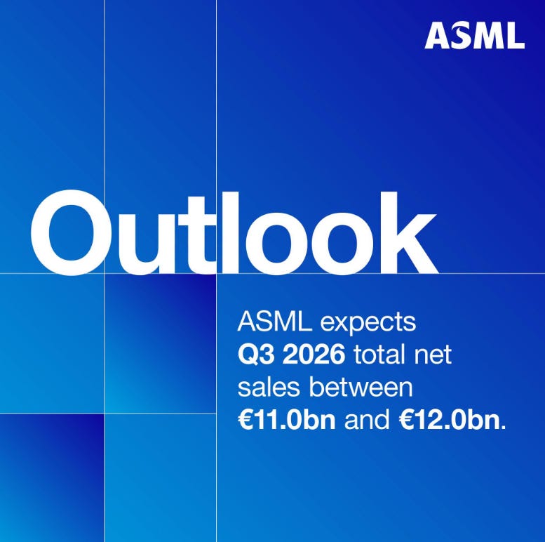
The company reported second-quarter sales of €9.326 billion and net income of €2.918 billion. It raised its full-year 2026 revenue outlook from €36–40 billion to €43–45 billion, with an expected gross margin of 54–56%. More importantly, ASML said continued AI investment was driving demand for advanced logic and memory chips, prompting customers to accelerate capacity expansion and make longer-term commitments across its product portfolio.
The message is larger than the financial revision.
AI is no longer constrained primarily by how many chips customers want to purchase. It is increasingly constrained by how quickly the semiconductor industry can build the capacity to manufacture them.
The Bottleneck Is Moving Upstream
During the first stage of the generative AI boom, the most visible shortage was GPUs. Cloud providers competed for NVIDIA accelerators, lead times expanded and allocation became strategically important.
The constraint then shifted toward HBM.
AI accelerators required much greater memory bandwidth, but HBM output was limited by advanced DRAM wafer capacity, stacking yields, bonding equipment and testing throughput. The next bottleneck appeared in advanced packaging, especially the capacity needed to integrate accelerators, HBM stacks, silicon interposers and substrates into complete systems.
ASML’s latest outlook suggests that the constraint is now moving another layer upstream.
The industry must secure enough EUV capacity to support the expansion of 2nm-class logic and advanced DRAM. At the same time, customers must determine when and where High-NA EUV can economically replace increasingly complex Low-NA multi-patterning.
This is a more fundamental constraint than the shortage of an individual chip.
A GPU shortage can eventually be addressed by reallocating additional wafer and packaging capacity. An EUV shortage affects the industry’s ability to create that wafer capacity in the first place.

ASML said its 2026 Low-NA EUV production capacity is approximately 65 systems. The company plans to add 30% in 2027 and is evaluating another 30% increase for 2028. It is also planning a similar expansion in DUV immersion capacity from a 2026 base of approximately 130 systems.
The scale and timing of this expansion suggest that customers are not planning only for current AI products. They are reserving manufacturing capability for the 2027–2029 technology roadmap.
Below we will share:
Low-NA Will Carry the Near-Term AI Expansion
High-NA Is About Process Simplification, Not Resolution Alone
The ASML Supply Chain: Where Value Could Spread (5 companies)
What the Market Should Watch Next

5月28日

2025年8月25日
Low-NA Will Carry the Near-Term AI Expansion
Although High-NA receives more attention because of its technical novelty, Low-NA EUV will remain the workhorse of advanced semiconductor manufacturing for the next several years.

ASML’s NXE:3800E is designed to support high-volume production of 2nm logic and leading-edge DRAM. Its demonstrated throughput has increased from 220 to 230 wafers per hour, while the future NXE:3800F is now targeted at 260 wafers per hour around 2028. ASML is also developing a higher-power source that could extend Low-NA productivity toward 330 wafers per hour by 2031.
This matters because the first wave of 2nm production does not depend on High-NA.
TSMC began N2 volume production in the fourth quarter of 2025 and is ramping the node across Hsinchu and Kaohsiung for smartphone and HPC applications. N2P is scheduled for volume production in the second half of 2026. These ramps are fundamentally based on the existing Low-NA EUV ecosystem, supplemented by immersion lithography, computational patterning and increasingly sophisticated process control.
High-NA is therefore not replacing Low-NA immediately. It is creating an additional option for the most difficult layers of future nodes.
The strategic issue is not whether one platform wins and the other disappears. It is how chipmakers optimise the combination of Low-NA single exposure, Low-NA multi-patterning and selective High-NA insertion.

ASML’s EUV Capacity Roadmap
ASML said it had shipped eight High-NA systems by the end of 2025, with six in operation, including the first second-generation EXE:5200B. The company expects the platform to meet high-volume manufacturing requirements by the end of 2026, with customer insertion during 2027–2028.
These targets should be treated as a roadmap rather than a guarantee. Actual insertion will depend on tool availability, mask infrastructure, photoresist performance, defect control, overlay, cycle time and customer-specific process economics.
High-NA Is About Process Simplification, Not Resolution Alone
High-NA EUV increases numerical aperture from 0.33 to 0.55, improving imaging resolution and potentially allowing difficult patterns to be printed with fewer exposures.
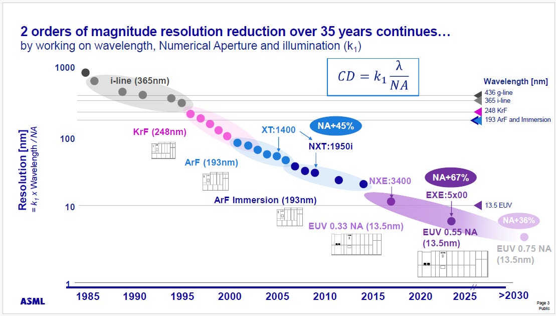
The economic case is not simply that High-NA can print smaller features. Its value lies in reducing patterning complexity.
ASML said logic and DRAM customers had presented examples in which High-NA could replace a three-mask EUV sequence with one mask and reduce certain patterning modules from approximately 100 process steps to around 10. Such simplification could shorten cycle times, reduce overlay risk and lower the cumulative defect opportunities created by repeated deposition, lithography and etching.
However, High-NA introduces its own challenges.
The anamorphic optical architecture changes field dimensions and creates new requirements around mask design, stitching, resist sensitivity, pellicles, inspection and metrology. Customers must therefore evaluate the cost of a High-NA exposure against the cost of multiple Low-NA exposures and the additional process steps surrounding them.
High-NA adoption will consequently be layer-selective.
Chipmakers are unlikely to move every EUV layer to High-NA. They will initially target the layers where pattern simplification, overlay improvement or yield benefits justify the higher tool and ecosystem cost.
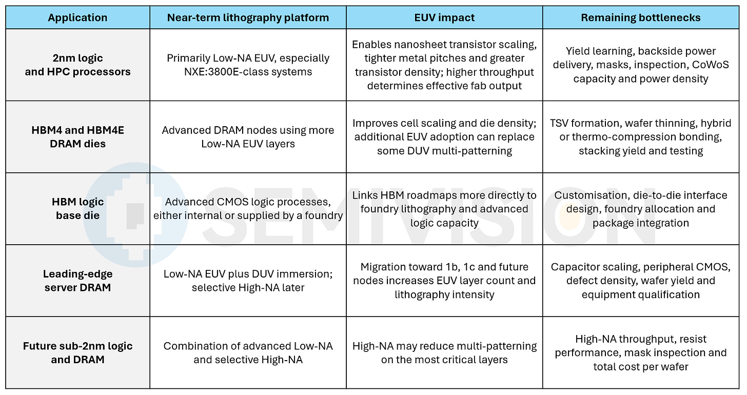
How EUV Expansion Affects 2nm, HBM and DRAM
ASML has said memory customers are ramping 1b and 1c DRAM while increasing the number of EUV layers and converting some DUV multi-patterning into EUV single exposure. The company expects lithography intensity to continue increasing as DRAM architectures become more complex.
For HBM, the impact is broader than the DRAM cell process.
SK hynix is applying advanced logic technology to the HBM base die through its collaboration with TSMC, while Micron has described HBM4 as using advanced CMOS and metallisation processes on both the base logic die and DRAM core dies. This means future HBM increasingly combines memory manufacturing, logic-foundry capacity and advanced packaging in a single supply-chain roadmap.
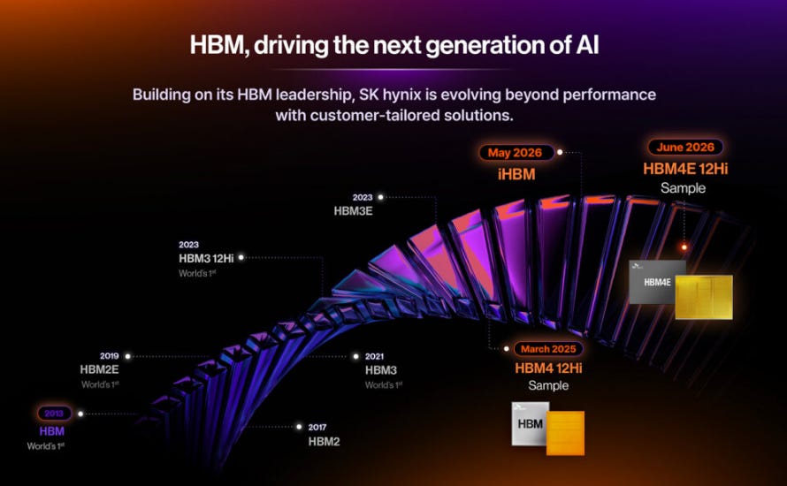
The result is a tighter interdependence between foundry and memory investment.
A memory company may have sufficient DRAM wafer capacity but still be constrained by base-die supply or stacking yield. A foundry may expand AI accelerator output but remain limited by HBM availability. EUV expansion relieves only one part of this interconnected system.
The ASML Supply Chain: Where Value Could Spread
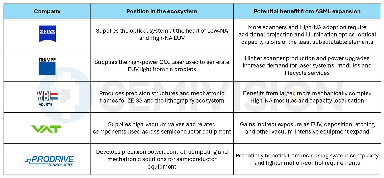
ASML is the system integrator, but an EUV scanner depends on a highly specialised European and global supplier network. The system combines advanced optics, high-power lasers, precision structures, vacuum equipment, motion control, masks, resists and inspection platforms.
The most visible beneficiaries can be divided into three groups.
Core EUV System Suppliers

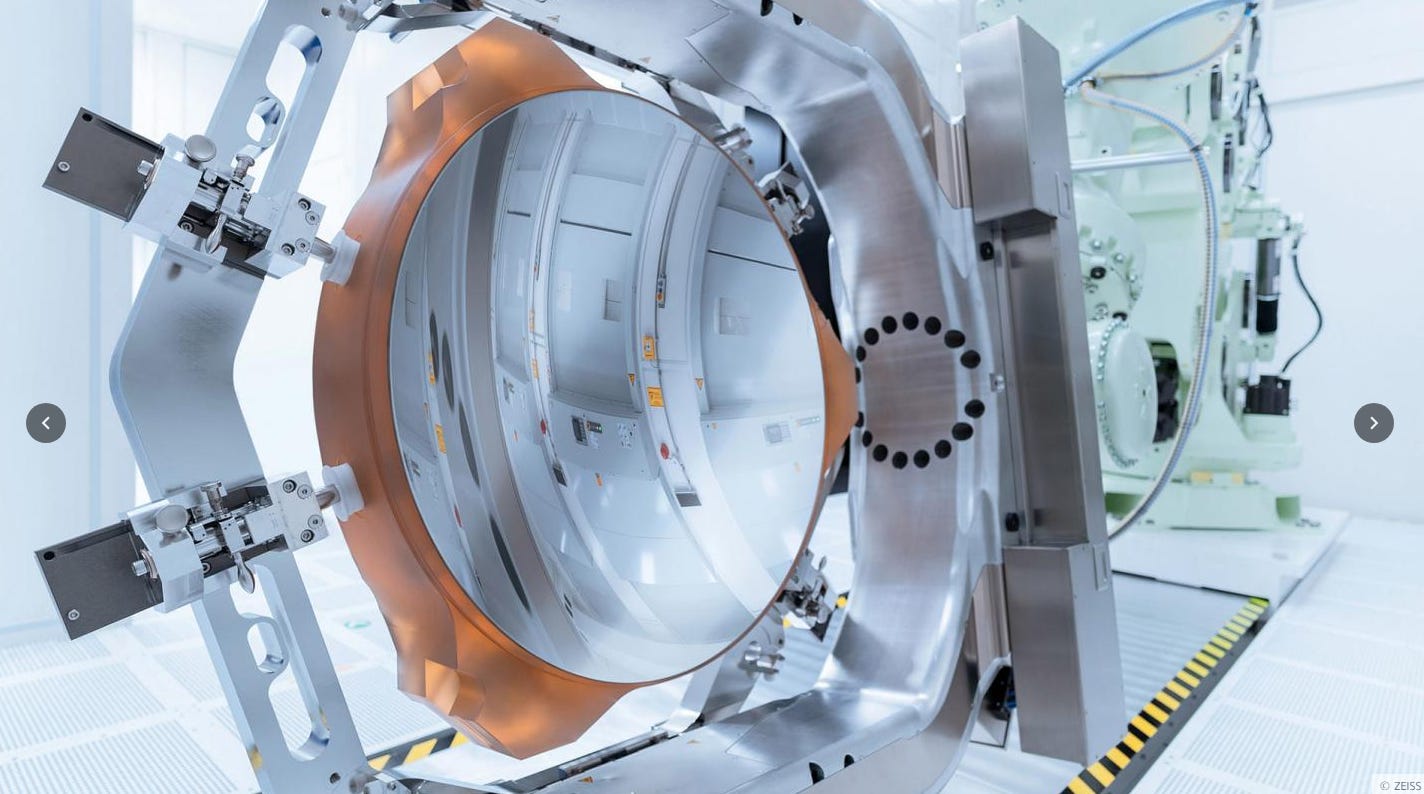
ZEISS describes its optical system as the core of High-NA EUV, while TRUMPF supplies the high-power laser that creates the 13.5nm light source. VDL has disclosed that it manufactures precision frames used to support and position ZEISS mirrors for next-generation ASML systems.
VAT’s exposure is broader and less ASML-specific, but high-vacuum valves are mission-critical across lithography and other wafer-fabrication tools. Prodrive similarly offers power, motion, imaging and control systems across front-end and back-end semiconductor equipment rather than disclosing a pure EUV revenue stream
EUV Masks, Inspection and Process Control
The second beneficiary group is not necessarily inside the scanner.
High-NA adoption increases the importance of mask blanks, mask inspection, actinic qualification, wafer metrology and defect control. As pattern dimensions become smaller, a defect that was previously tolerable can become yield-limiting.
Lasertec is particularly exposed to EUV mask infrastructure. The company offers actinic inspection systems for EUV mask blanks, patterned masks and pellicles, including systems that inspect defects using the same 13.5nm wavelength employed in EUV exposure.

ZEISS also provides AIMS EUV systems for actinic mask qualification, with its latest platform supporting both Low-NA and High-NA scanner matching.

AIMS® EUV 3.0: ZEISS SMT extends global footprint in actinic mask qualification
As High-NA moves toward production, inspection spending may increase faster than scanner unit growth because customers must control defects across masks, pellicles, wafers and increasingly complex patterning flows.
This category may be less visible but strategically important. High-NA requires resists capable of balancing resolution, sensitivity and line-edge roughness. Higher source power and scanner throughput also increase requirements for contamination control, thermal stability and component lifetime.
This creates a second growth engine alongside new equipment deliveries.
Not Every Supplier Is an Equal Beneficiary
The supply-chain opportunity should not be interpreted too broadly.
A company can participate in semiconductor equipment without having meaningful EUV exposure. It can also experience rising revenue while facing capacity investments, customer concentration or margin pressure.
The strongest positions are likely to belong to suppliers with four characteristics:
Technology that is difficult to substitute.
Qualification cycles that take years rather than months.
Content that increases as scanner performance rises.
Recurring service or replacement demand after installation.
ZEISS and TRUMPF represent highly strategic positions, but both are privately held. Among publicly traded companies, VAT Group and Lasertec provide more visible exposure to vacuum and EUV inspection respectively, although neither should be treated as a pure proxy for ASML’s revenue.
The more relevant investment question is not simply which companies supply ASML.
It is which suppliers gain additional content per system, retain pricing power and avoid being reduced to commodity manufacturing as EUV volume expands.
EUV Does Not Eliminate the Next Bottleneck
Even if ASML successfully expands EUV output, AI infrastructure could remain constrained elsewhere.

More advanced wafers require more HBM, packaging, substrates and testing. Larger AI packages create greater warpage and thermal-management challenges. More servers require higher-density power conversion, advanced MLCCs, optical interconnects, liquid cooling and access to utility-scale electricity.
The supply chain is therefore unlikely to become unconstrained.
The bottleneck will migrate.
If EUV capacity improves faster than CoWoS, hybrid bonding or HBM stacking, the constraint will move downstream. If packaging capacity expands, pressure could shift toward substrates, silicon photonics, power delivery or cooling.
This is the defining characteristic of the AI semiconductor cycle: demand is scaling across an entire system, but supply expands one layer at a time.
What the Market Should Watch Next
The first indicator is actual Low-NA system output rather than order announcements. ASML must coordinate its own assembly operations with optics, lasers, precision structures and thousands of specialised components.
The second is customer installation readiness. An EUV scanner does not create productive capacity until the fab, utilities, process modules, masks and engineering teams are ready.
The third is High-NA throughput, availability and yield. High-NA’s commercial importance will depend less on maximum resolution than on cost per usable wafer.
The fourth is the balance between front-end and back-end investment. If advanced wafer capacity grows faster than packaging, bonding and testing, AI chip output will remain constrained.
The fifth is whether EUV demand from DRAM becomes structurally stronger. Continued migration from DUV multi-patterning toward EUV single exposure would make memory an increasingly important source of lithography intensity.
Finally, the market should monitor whether ASML’s suppliers can expand at the same rate as ASML itself. The scanner manufacturer may announce a 30% capacity increase, but the actual ramp will depend on whether its most specialised partners can deliver compatible growth.

From Chip Demand to Manufacturing Capability
The most important message from ASML’s July 15 update is not that an equipment company expects to generate more revenue.
It is that the AI semiconductor cycle has entered a deeper supply race.
The first phase was defined by GPU demand. The second was defined by HBM and advanced-packaging shortages. The next phase will be defined by the ability to build, qualify and operate the manufacturing capacity required for the entire AI infrastructure stack.
Low-NA EUV will carry the near-term expansion of 2nm logic and advanced DRAM. High-NA will gradually enter the layers where process simplification can justify its higher cost and ecosystem complexity.
The winners will not necessarily be the companies announcing the largest capital-expenditure budgets.
They will be the companies that secure equipment early, prepare their fabs on time, validate processes quickly and coordinate advanced logic, memory and packaging into reliable customer deliveries.
For SemiVision readers, it is therefore no longer enough to monitor GPU shipments or one foundry’s monthly revenue.
The higher-value question is how the entire semiconductor supply chain is translating AI demand into repeatable, scalable and durable manufacturing capability.
ASML’s raised outlook is one of the clearest signs yet that this new phase has already begun.


PreviousNext