UMC and SILITH Bring 12-Inch Silicon Photonics to Mass Production as AI Interconnect Competition Enters the Industrial Scale-Up Era
UMC and SILITH Bring 12-Inch Silicon Photonics to Mass Production as AI Interconnect Competition Enters the Industrial Scale-Up Era
- Source: SemiVision
- Author: SEMIVISION
- Published: 2026-07-15T16:03:32+08:00
- URL: https://tspasemiconductor.substack.com/p/umc-and-silith-bring-12-inch-silicon (6) UMC and SILITH Bring 12-Inch Silicon Photonics to Mass Production as AI Interconnect Competition Enters the Industrial Scale-Up Era


UMC and SILITH Bring 12-Inch Silicon Photonics to Mass Production as AI Interconnect Competition Enters the Industrial Scale-Up Era
Original Article By SemiVision Research [Reading time: 21 mins]

Jul 15, 2026
∙ Paid
UMC and SILITH Bring 12-Inch Silicon Photonics to Mass Production as AI Interconnect Competition Enters the Industrial Scale-Up Era

On July 14, 2026, UMC and Singapore-based silicon photonics company SILITH announced that they had completed delivery of the first batch of mass-produced silicon photonic wafers from UMC’s 12-inch fab in Singapore.
On the surface, this is a milestone marking the transition of a silicon photonics product into volume production. From a semiconductor supply chain perspective, however, its significance is much broader. It suggests that silicon photonics is beginning to cross one of its most persistent barriers: moving beyond laboratory demonstrations and exhibition-stage prototypes into industrial-scale manufacturing with predictable cost, yield, reliability, and delivery schedules.

UMC delivers first mass-produced silicon photonics wafers from UMC’s Singapore 12-inch fab, marking a step change from development to high-volume manufacturing.
The collaboration combines SILITH’s silicon photonics innovation with UMC’s high-volume 12-inch manufacturing platform.
UMC’s silicon photonics process integration is a scalable, foundry-ready manufacturing platform—aimed at delivering predictable cost, yield, and ramp timelines for customers building next-generation AI data center optical interconnects
The collaboration combines SILITH’s silicon photonics architecture with UMC’s 12-inch process-integration capabilities to support 1.6Tbps optical interconnect products. According to the two companies, it took only 18 months to move from platform development to mass-production introduction. The platform has now reached the yield and reliability levels required for commercial manufacturing and has passed qualification by a leading global cloud infrastructure customer.
UMC also plans to officially launch its own 12-inch silicon photonics platform in 2027, opening it to additional customers for product development and volume manufacturing.
This means UMC is no longer participating in the AI cycle only as a mature-node foundry. It is beginning to move into one of the fastest-growing and most manufacturing-intensive parts of AI infrastructure: optical interconnects.

2025年4月6日
Why This Milestone Matters More Than the “1.6T” Headline
The silicon photonics industry has never lacked high-speed device demonstrations.
Over the past several years, companies have shown 100G, 200G, and even 400G-per-lane modulators, photodetectors, and optical engines. But producing a high-speed device in a laboratory is not the same as manufacturing it consistently in a foundry. Achieving a target specification on a single chip does not guarantee that thousands of wafers and millions of devices will deliver the same optical performance.
The largest barriers to silicon photonics commercialization are often not whether a device can reach a certain speed, but whether several manufacturing challenges can be solved simultaneously.
Can process variation be controlled? Are optical characteristics consistent across a wafer and from wafer to wafer? Can coupling efficiency, insertion loss, polarization sensitivity, and wavelength drift remain within production specifications? After the photonic chip is assembled with drivers, DSPs, lasers, and optical fibers, does the total module yield still make economic sense?
The real achievement of UMC and SILITH is that they have moved these questions from the R&D stage into customer qualification and first-batch volume delivery.
UMC has emphasized that the platform can provide predictable cost, yield, and production schedules. That statement may be more important than the 1.6T data rate itself. It indicates that the collaboration is not centered on a single demonstration chip, but on building a manufacturing process that can be repeated, scaled, and continuously improved.
Below we will share:
Who Is SILITH? It Is Not Merely a Single-Device Silicon Photonics Company
SILITH’s Technology Core
Why the Move to 12-Inch Wafers Is Essential
Supply Chain Layer 1 to 5
Singapore Is Emerging as an Asian Silicon Photonics Manufacturing Cluster
Implications for Taiwan’s Supply Chain
UMC’s Readiness for Silicon Photonics & TFLN

3月5日

2025年11月29日
Who Is SILITH? It Is Not Merely a Single-Device Silicon Photonics Company
Founded in 2021 and headquartered in Singapore, SILITH focuses on AI infrastructure, high-speed data-center connectivity, and photonic integrated circuits.
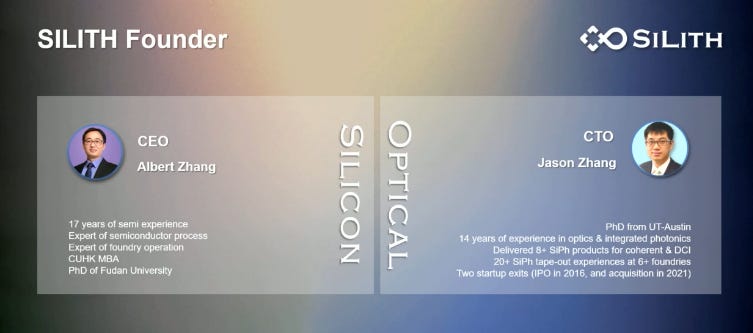
According to information released by UMC, SILITH’s 100G- and 200G-per-lane silicon photonic PICs are already in commercial production, with cumulative shipments exceeding eight million units.
That shipment record is important.
Silicon photonics startups can generally be divided into two categories. Some are built around a single high-performance device or material. Others are attempting to establish a broader photonics platform. SILITH appears closer to the second category.
Its portfolio covers direct-detection data-center optics, coherent communications, optical sensing, and architectures ranging from pluggable optical modules and co-packaged optics to future optical I/O.
SILITH has listed products including 1.6T DR8 transmitter PICs, 1.6T FR4 transmitter PICs, dual-FR4 receiver PICs, and 1.6T coherent receivers. This indicates that the company is not tying its technology to a single fiber or module architecture. Instead, it is trying to extend the same silicon photonics foundation across parallel optics, wavelength-division multiplexing, and coherent optical communications.

In 2025, SILITH also presented at the Open Compute Project Europe Summit under the theme “Industrialize Silicon Photonics to Mass Production.” The title itself reveals the company’s core strategy. SILITH is not focused only on achieving the highest laboratory bandwidth. Its central objective is to move silicon photonics into real industrial-scale manufacturing.

SILITH’s Technology Core: High-Speed MZMs for 200G and 400G per Lane
One of the most important elements of SILITH’s technology roadmap is the high-speed Mach–Zehnder modulator, or MZM.
An optical modulator converts high-speed electrical signals from a driver chip into optical signals. As AI clusters move from 800G to 1.6T, 3.2T, and eventually higher bandwidths, increasing the data rate of each optical lane becomes an important way to reduce fiber count, packaging complexity, and cost per bit.
Public technical information from SILITH indicates that its proprietary high-speed silicon MZM and hybrid-polymer modulator technologies can support bandwidths above 70GHz, while the silicon MZM has a Vπ·L value below 1.5 V·cm.
Vπ·L is commonly used to measure modulator efficiency. A lower value generally means that a lower driving voltage or a shorter device length is required to achieve the same optical phase shift. This can help reduce driver power consumption and chip area.
UMC and SILITH have already commercialized a customized 200G-per-lane silicon photonics process. The next phase is the joint development of a 400G-per-lane pure-silicon photonics platform.
The platform will continue to use high-speed silicon MZMs, with the goal of achieving 400G-per-lane transmission while maintaining compatibility with CMOS manufacturing processes.
At OFC 2026, SILITH also presented a 400G-per-lane platform that included a pure-silicon MZM transmitter and germanium photodetectors with a 3dB bandwidth exceeding 110GHz.

This suggests that the company’s 400G roadmap is not limited to the transmit side. SILITH is attempting to build both transmit and receive capabilities, as well as a complete optical link architecture.
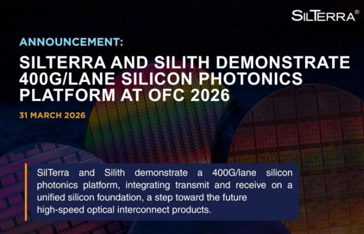
Advancing the future of high-speed connectivity.
In collaboration, SilTerra and Silith have demonstrated a 400G/lane silicon photonics transmit-and-receive platform—integrating both transmitter and receiver on a unified silicon foundation at OFC 2026 recently.
This milestone marks a significant step toward scalable, next-generation optical interconnect solutions.
1.6T Is Not a Single-Device Speed; It Is a System-Engineering Problem
A 1.6T optical link delivers an aggregate data rate of 1.6 terabits per second, but it is usually not achieved through a single optical lane.
In a 200G-per-lane architecture, eight 200G lanes can form a 1.6T link. These lanes may be configured in different ways. DR8 uses eight parallel optical channels, while FR4 uses wavelength-division multiplexing to place four wavelengths on a single fiber. Two FR4 groups can together form a 1.6T solution.
As a result, the competitiveness of a 1.6T product is not determined only by modulator speed.
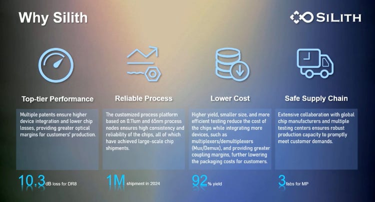
It also depends on multiplexer and demultiplexer loss, wavelength control, laser power, driver and TIA bandwidth, DSP algorithms, fiber-coupling accuracy, packaging thermal stability, and the total system bit-error rate.
SILITH’s simultaneous development of DR8 and FR4 products suggests that it is not betting on a single module standard. Instead, it is building PIC platforms that can support different switch architectures, fiber infrastructures, and data-center network topologies.
This flexibility matters to cloud customers because scale-out networks, scale-up networks, and data-center interconnects have different requirements for reach, power consumption, fiber count, and serviceability.
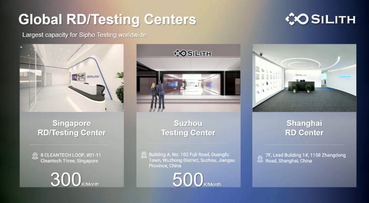
Why the Move to 12-Inch Wafers Is Essential
Silicon photonics is widely regarded as one of the optical platforms with the greatest potential for large-scale adoption because it can leverage the existing semiconductor manufacturing infrastructure.
UMC is using 12-inch wafers and silicon-on-insulator, or SOI, manufacturing capabilities for this platform. The thin silicon layer in an SOI wafer can be used to form optical waveguides, splitters, couplers, and modulators, while the buried oxide layer helps confine light within the waveguide structure.
The value of 12-inch manufacturing is not limited to producing more dies per wafer.
More importantly, it allows silicon photonics to use the semiconductor industry’s existing automation equipment, statistical process control, defect-management systems, process analytics, and supply chain scale.
However, silicon photonics is not simply a direct copy of conventional electronic-chip manufacturing.
Minor roughness on the sidewall of an optical waveguide can increase scattering loss. Variations in etch depth and line width can change the effective refractive index. Ion-implantation concentration can affect modulation efficiency and resistance. Germanium epitaxy quality influences photodetector bandwidth and dark current. Small dimensional shifts in optical couplers can also materially affect coupling tolerance and insertion loss.
In other words, electronic-chip production is primarily concerned with electrical parameters. Silicon photonics manufacturing must simultaneously control geometry, materials, electrical behavior, and optical response.
The fact that UMC and SILITH completed platform introduction within 18 months suggests that SILITH’s device designs and UMC’s process modules have already undergone a meaningful degree of design–technology co-optimization.
This type of co-development capability is likely to become one of the most important competitive barriers in silicon photonics foundry services.
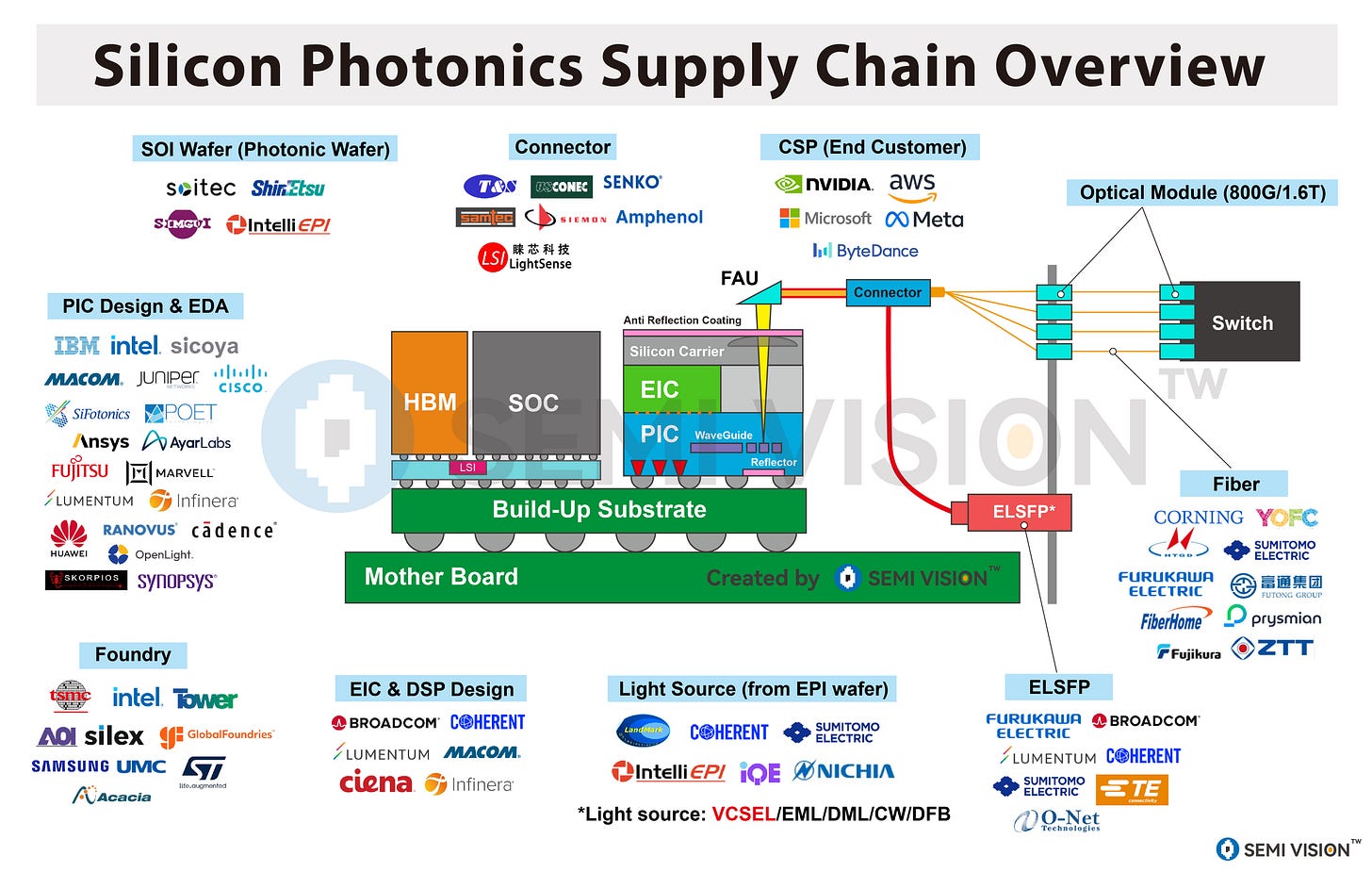
Supply Chain Layer One: SOI Wafers, Photomasks, Materials, and Process Equipment
Once silicon photonics enters mass production, it creates a supply chain that looks increasingly similar to semiconductor manufacturing rather than the traditional optical-module industry.
The first upstream component is the SOI wafer.
Silicon-layer thickness, wafer uniformity, buried-oxide quality, and defect density can directly affect waveguide and active-device performance. As the industry migrates from 8-inch to 12-inch production, stable access to high-quality 12-inch SOI wafers will become a critical condition for capacity expansion.
The next layer includes photomasks, photoresists, etching gases, thin-film deposition, ion implantation, and germanium epitaxy.
Silicon photonics may use relatively mature logic-node equipment, but the dimensional and profile requirements of certain structures are still demanding. Waveguide sidewall quality, the positioning of PN junctions inside modulators, and interface defects in germanium photodetectors can all affect final optical yield.
Silicon photonics should therefore not be treated as a low-cost mature-node process.
It is better understood as a highly customized specialty-process platform whose value comes from integrating optical, electrical, material, and manufacturing expertise.
Supply Chain Layer Two: PDKs, EDA, and Electronic–Photonic Co-Design
For a silicon photonics platform to evolve from a customized process for one customer into a foundry platform that can serve multiple customers, it must establish mature process design kits, device models, and design rules.
Traditional electronic IC design focuses primarily on transistors, interconnects, timing, and power. Silicon photonics design must also simulate optical propagation, coupling, reflection, polarization, wavelength behavior, and thermal drift.
When a PIC is packaged together with a driver, TIA, or DSP, the design team must also perform joint electrical and optical simulation.
This means that the competitiveness of UMC’s planned 2027 platform will depend not only on device speed.
The market will also evaluate the completeness of its PDK, the availability of reusable IP, its multi-project-wafer services, its compatibility with EDA tools, and its reference packaging flows.
The larger strategic opportunity is to create a design-to-manufacturing feedback loop.
Device models and PDKs guide the initial design. Wafer-level optical and electrical test results then feed back into the models, enabling faster yield learning and shorter time to production.

2025年6月22日
Supply Chain Layer Three: Lasers, Drivers, TIAs, and DSPs Remain Essential
The term “pure-silicon photonics platform” can create the mistaken impression that the entire optical communication system can be built using silicon alone.
That is not the case.
Silicon is an indirect-bandgap material and is not efficient at generating light. Most silicon photonics systems therefore still require external lasers, III-V laser chips, or heterogeneous integration of materials such as indium phosphide with the silicon platform.
In addition, MZMs require high-speed driver ICs. Photodetectors at the receiver need TIAs to amplify the electrical signal. High-speed PAM4 links generally require DSPs for equalization, clock recovery, and error correction.
The mass production of SILITH PICs at UMC will therefore not replace the existing optical-communications electronics supply chain.
Instead, it will increase the need for co-design across PICs, DSPs, drivers, TIAs, and laser sources.
The future competitive unit will no longer be a single chip. It will be the complete optical engine.
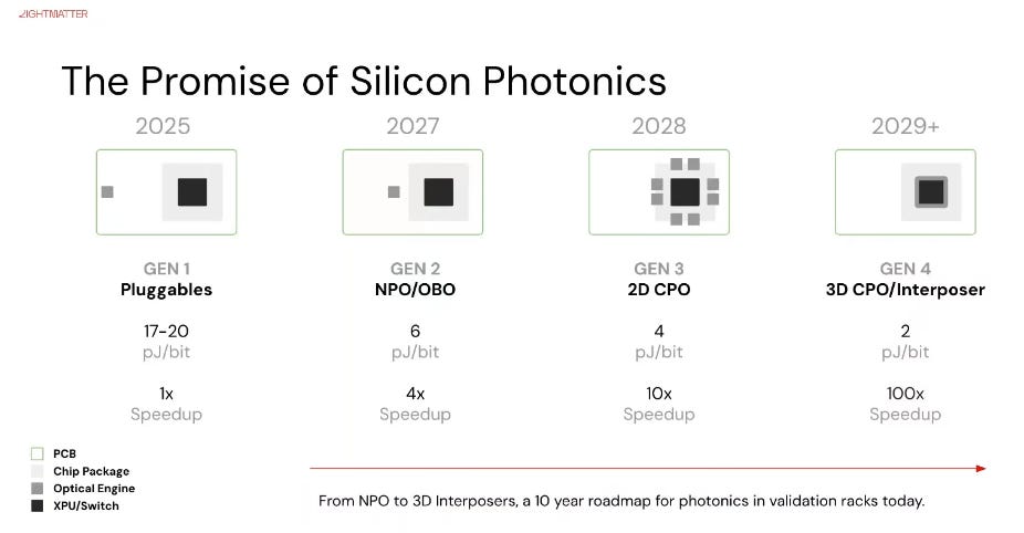
The winning suppliers will be those that can integrate lasers, PICs, electronic ICs, fibers, and thermal structures into the smallest possible footprint while achieving low power consumption and high assembly yield.
Supply Chain Layer Four: Advanced Packaging Will Determine Whether CPO Can Scale
SILITH’s technology roadmap covers pluggable optical modules, co-packaged optics, and future optical I/O.
Moving from pluggable optics to CPO means relocating optical components from the front panel of a switch closer to the switch ASIC. This shortens the distance over which high-speed electrical signals must travel across the PCB, reducing SerDes power consumption and channel loss.
But it also significantly increases packaging complexity.
CPO must address not only die attachment, but also fiber-array alignment, laser-source placement, thermal isolation, contamination at optical interfaces, package warpage, serviceability, and long-term reliability.
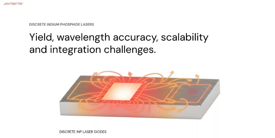
The PIC itself may use a mature process, but the switch ASIC or AI computing chip packaged alongside it will often use an advanced logic node.
If the PIC, electronic IC, or fiber assembly fails after packaging, the entire high-value module may need to be discarded rather than a single low-cost photonic die.
This is why the silicon photonics supply chain will increasingly overlap with advanced packaging, hybrid bonding, flip-chip assembly, substrates, fiber coupling, and thermal management.
UMC has also indicated that its future silicon photonics and thin-film lithium niobate platforms will be combined with advanced packaging capabilities to support CPO and optical I/O.
This suggests that UMC’s ambition extends beyond wafer fabrication. It is gradually building a technology roadmap from photonic processes to system-level integration.
Supply Chain Layer Five: Testing May Become a Bigger Bottleneck Than Wafer Fabrication
As silicon photonics moves into volume production, test throughput and cost will become critical issues.
Electronic chips can be tested rapidly through probe cards that contact large numbers of pads. Photonic chips require light to be accurately coupled into the device before insertion loss, responsivity, bandwidth, and bit-error rate can be measured across different wavelengths, optical powers, and polarization conditions.
Aligning a fiber to a grating coupler typically requires precision motion control. Each realignment, wavelength sweep, or polarization adjustment adds test time.
If every PIC requires a comprehensive optical scan, test-equipment throughput may not keep pace with wafer-fab capacity.
This creates demand for automated fiber alignment, simultaneous optical and electrical testing, wafer-level probing, high-speed optical instrumentation, and integrated test software.
For the supply chain, silicon photonics mass production will therefore drive demand not only for wafer-fabrication equipment, but also for tunable lasers, polarization controllers, optical power meters, optical network analyzers, high-speed oscilloscopes, automated optical probes, and specialized test software.
The companies that deliver the greatest improvements in production yield may not come only from the optical-communications industry. They may also come from semiconductor testing and precision-automation suppliers.

5月25日
Singapore Is Emerging as an Asian Silicon Photonics Manufacturing Cluster
The fact that this production milestone occurred at UMC’s Singapore facility is also strategically significant from a supply chain geography perspective.
UMC has stated that its Singapore site is not only a 12-inch manufacturing base, but also an important technology-development center. This has allowed UMC and SILITH to accelerate process debugging, wafer analysis, and qualification.
SILITH is also headquartered in Singapore, and the geographic proximity between the design company and the foundry can reduce development cycles and improve collaboration during manufacturing introduction.
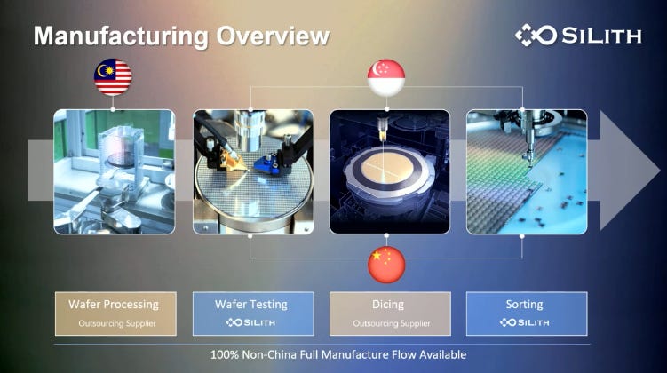
At the same time, GlobalFoundries already provides 8-inch and 12-inch silicon photonics manufacturing in Singapore and strengthened its local capabilities by acquiring Advanced Micro Foundry in 2025.
SILITH has also previously demonstrated a 400G-per-lane silicon photonics transceiver platform with Malaysia-based SilTerra.
Combined with its current work with UMC on 1.6T production and 400G-per-lane development, this suggests that SILITH may be following a multi-foundry strategy, assigning different devices, product generations, or customer requirements to different manufacturing platforms.
This is a reasonable industry inference rather than a formally announced SILITH supply strategy.
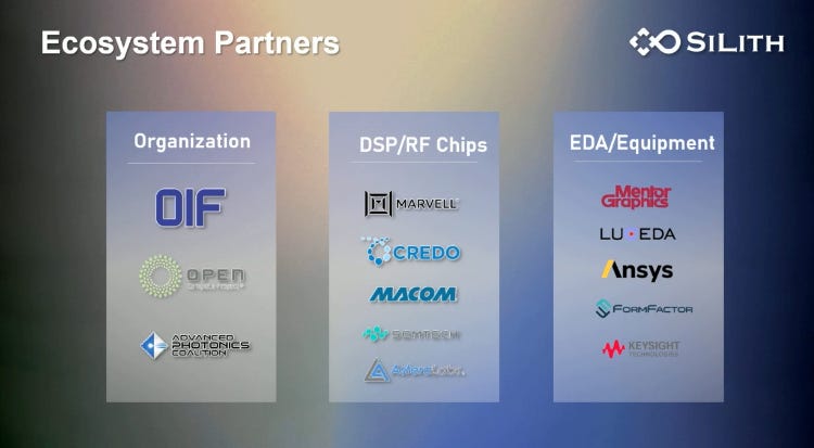
More broadly, Singapore and Malaysia are beginning to form a regional cluster that brings together silicon photonics design companies, foundries, OSAT providers, and optical-communications manufacturers.
For UMC, participation in this cluster provides an opportunity to avoid competing with TSMC solely through advanced logic nodes. Instead, it can enter the AI supply chain through specialty processes, silicon photonics, and cross-domain integration.
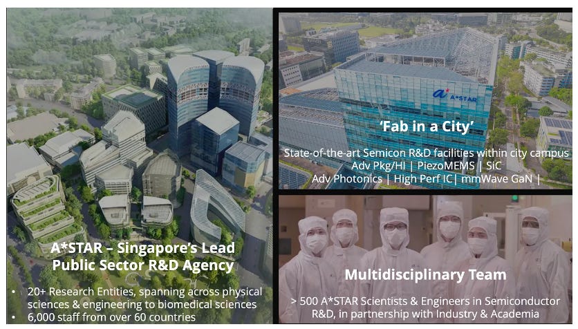
ASTAR, Singapore’s Agency for Science, Technology and Research, is the country’s leading public-sector R&D organization. Through more than 20 research entities spanning the physical sciences, engineering and biomedical sciences, ASTAR connects scientific discovery with industrial innovation and economic development. Its international workforce includes around 6,000 employees from over 60 countries, creating a highly multidisciplinary research environment.
In semiconductors, ASTAR operates advanced “Fab in a City” research facilities within Singapore’s urban innovation ecosystem. These platforms support work in advanced packaging, piezoelectric MEMS, silicon carbide, advanced photonics, high-performance integrated circuits and millimeter-wave gallium nitride technologies. More than 500 scientists and engineers contribute to semiconductor R&D, working closely with industry partners, universities and government agencies. By combining research infrastructure, engineering expertise and commercialization capabilities, ASTAR helps accelerate technology transfer, strengthen Singapore’s semiconductor supply chain and position the country as a strategic hub for next-generation electronics, advanced manufacturing and deep-tech innovation.

2025年6月21日
Implications for Taiwan’s Supply Chain: The Opportunity Extends Far Beyond Foundry Manufacturing
The significance of the UMC–SILITH collaboration for Taiwan should not be reduced to the addition of one specialty process.
As silicon photonics moves from pluggable modules toward CPO and optical I/O, Taiwan’s existing strengths in semiconductor manufacturing, advanced packaging, substrates, testing, thermal management, and server systems could all become part of the new supply chain.
Potential beneficiaries include suppliers of:
SOI and specialty wafers; thin-film deposition and etching equipment; photomasks and process chemicals; silicon photonics EDA tools and IP; lasers and photodetectors; high-speed drivers and TIAs; DSPs and switch ASICs; flip-chip and heterogeneous integration; fiber arrays and precision coupling; wafer-level optical testing; and thermal-management and reliability solutions for CPO modules.
However, Taiwan’s supply chain must also recognize a fundamental difference.
Silicon photonics cannot be developed vertically by a single industry.
Electronic IC engineers, optical engineers, packaging engineers, material scientists, and system architects must work together. Taiwan’s supply chain has traditionally been highly effective at rapidly scaling a mature customer design.
Silicon photonics requires suppliers to enter the development process earlier and jointly define device, packaging, test, and reliability specifications.
The supplier’s role will therefore shift from manufacturing to an existing specification toward helping the customer define the specification.
2025 Version
Four Risks the Market Should Continue to Monitor
The first risk is that first-batch volume delivery does not automatically mean broad-scale ramp-up.
UMC and SILITH have not disclosed wafer volumes, product ASPs, capacity allocation, specific production yields, or expected revenue contributions.
High yield and customer qualification are important milestones, but investors still need to monitor follow-on orders and expansion schedules before assuming material revenue growth.
The second risk is that 400G per lane remains a next-stage development target.
The core commercialized products today are still based on 100G and 200G per lane.
A 400G-per-lane pure-silicon MZM platform, thin-film lithium niobate, and denser optical I/O architectures will still require device-level, package-level, DSP-level, and system-level validation.
The third risk is that a pure-silicon platform does not mean a simple supply chain.
Silicon MZMs can preserve CMOS process compatibility, but the complete optical engine still requires lasers, driver ICs, receive electronics, fibers, and packaging.
A supply, yield, or reliability problem in any of these components can constrain total system shipments.
The fourth risk is that the technical advantages of CPO do not guarantee rapid market adoption.
CPO still needs to solve issues involving laser lifetime, module serviceability, fiber management, thermal coupling, package testing, and industry standards.
In some applications, pluggable optics may retain a long life cycle because of their easier maintenance and more mature supply chain.

2025年6月16日
UMC’s Readiness for Silicon Photonics
UMC has been actively developing dedicated SiPh process technologies across multiple wafer sizes, ensuring a scalable and competitive manufacturing platform for photonic applications.
UMC’s SiPh Foundry Capabilities :6” TFLN PIC Technology:
UMC has developed Thin-Film Lithium Niobate (TFLN) PIC technology, known for its high-speed modulation and low optical loss.
Risk production began in 2024 at UMC, positioning UMC as an early leader in TFLN-based photonics.
8” Si PIC Technology: Since 2020, UMC has been mass-producing Si-based PICs at its 8D and 8F fabs, providing a mature and stable manufacturing platform.
12” Si PIC Platform for Next-Gen Photonic Interposers:
UMC officially kicked off 12” Si PIC production in Q1 2025 at its 12i fab, with an official announcement set for April 1, 2025.
This platform is designed to support photonic interposer solutions with TSV integration, enabling high-density optical-electrical co-packaging.

HyperLight, UMC, and Wavetek, a wholly owned subsidiary of UMC, today announced a strategic manufacturing partnership for high-volume foundry production of HyperLight’s TFLN (thin-film lithium niobate) Chiplet™ Platform on both 6-inch and 8-inch wafers. The collaboration marks a major inflection point in the commercialization of TFLN photonics, enabling the manufacturing capacity required for AI and cloud infrastructure deployment at scale.

HyperLight is a photonics company focused on enabling the mass deployment of thin-film lithium niobate, or TFLN, for high-performance optical systems. Founded in 2018 as a spinout rooted in more than a decade of research and development at Harvard, the company operates across Boston and Singapore.
HyperLight has shipped products to more than 100 customers in data communications, telecommunications, industrial equipment, and emerging technology markets. Its platform is designed for high-volume, CMOS-like manufacturing, supported by a foundry partnership with UMC. The company also works with a global and diversified network of Tier-1 supply-chain partners, helping it move from laboratory innovation toward scalable commercial production.
HyperLight’s intellectual-property portfolio includes more than 70 patents, with over 30 issued, more than 40 pending, and over 200 technical papers related to TFLN contributed by its team. This combination of technology, manufacturing scale, and ecosystem partnerships positions HyperLight as a key TFLN commercialization player.


UMC, a leading global semiconductor foundry, today announced a licensing agreement with imec, a world-leading research and innovation hub in advanced semiconductor technologies, for the transfer ofimec’s iSiPP300silicon photonics process, featuring co-packaged optics compatibility, to accelerate UMC’s silicon photonics roadmap. The licensed technology will enable UMC to bring a 12-inch silicon photonics platform to market targeting next-generation connectivity.


UMC’s 12” Advanced Packaging Capabilities
UMC is also advancing its 12” packaging capabilities to complement its SiPh foundry strengths:
Interposer Technology: Provides high-bandwidth, low-latency connectivity for SiPh module integration.
Deep Trench Capacitor (DTC) Solutions: Enhances power integrity and signal performance for high-speed optical applications.
DTC is a critical parameter in TSMC’s advanced packaging technologies. It is a recurring topic at TSMC’s Technology Symposiums, where ongoing enhancements to DTC performance are frequently highlighted. Currently, UMC also possesses the capability to develop and validate DTC solutions.
Chip-to-Wafer (C2W) and Co-Packaged Optics Integration: Enables seamless photonic-electronic co-packaging, reducing footprint and improving efficiency.
UMC’s Strategic Vision for Silicon Photonics
UMC is not just developing SiPh manufacturing capabilities—it is building a fully integrated SiPh ecosystem. Through its wafer-to-package solutions, UMC aims to:
Provide a standardized SiPh platform, reducing barriers for new entrants and accelerating product commercialization.
Scale up production for high-volume SiPh applications, from AI data centers to 5G/6G networks and optical computing.
Enable next-generation photonic interposers, setting the foundation for high-speed, low-power optical communication.
By leveraging its mature semiconductor expertise, advanced packaging technologies, and strategic partnerships, UMC is not just a SiPh foundry but a key enabler of the next-generation SiPh supply chain.
UMC’s Path to Becoming a SiPh Powerhouse
With its captive SiPh processes, scalable foundry solutions, and industry-leading advanced packaging technologies, UMC is poised to become a major force in the silicon photonics ecosystem.
By strengthening its SiPh manufacturing capabilities and enhancing packaging integration, UMC can provide a cost-efficient, high-performance SiPh platform that meets the needs of future AI, HPC, and optical networking applications.
As the 12” Si PIC platform launches in Q1 2025, UMC is taking a bold step toward reshaping the SiPh industry and establishing itself as a leader in the global photonics supply chain.
Conclusion: The Next Stage of AI Chip Competition Is About Moving Data
During the first phase of the AI semiconductor cycle, market attention focused primarily on GPUs, HBM, and advanced packaging.
But as the number of accelerators inside a single AI cluster continues to increase, the main system bottleneck is shifting.
The question is no longer only how much computation one chip can perform. It is increasingly about how quickly data can move between chips, racks, and data centers.
The completion of the first batch of 12-inch mass-produced silicon photonic wafers by UMC and SILITH indicates that silicon photonics is beginning to evolve from a high-performance optical technology into an industrial platform that can be manufactured at semiconductor scale.
SILITH contributes high-speed MZMs, 200G-per-lane products, 1.6T architectures, and a roadmap toward 400G per lane. UMC contributes SOI manufacturing, 12-inch capacity, process integration, yield management, and a future advanced-packaging platform.
Together, they are beginning to close one of the most important gaps in the silicon photonics industry: the manufacturing loop between design, process, testing, packaging, and system qualification.
The next key question is not whether SILITH can demonstrate another higher-speed device.
It is whether UMC can convert this customized collaboration into an open foundry platform with a mature PDK, reusable design IP, wafer-level testing, packaging solutions, and a broad customer base when it launches the platform in 2027.
If it succeeds, UMC will not simply be entering a new specialty-process segment.
It will be positioning itself in a manufacturing market that could eventually require billions of photonic devices across AI infrastructure.
The first half of the AI computing race was about manufacturing more and faster transistors.
The second half will be about moving the data generated by those transistors to the right place with the lowest possible power consumption.
Thanks for reading SEMIVISION @_@! This post is public so feel free to share it.

6月18日


Previous