TSMC’s Record June Revenue Signals a New AI Chip Pricing Supercycle
TSMC’s Record June Revenue Signals a New AI Chip Pricing Supercycle
- Source: SemiVision
- Author: SEMIVISION
- Published: 2026-07-14T11:00:46+08:00
- URL: https://tspasemiconductor.substack.com/p/tsmcs-record-june-revenue-signals (6) TSMC’s Record June Revenue Signals a New AI Chip Pricing Supercycle


TSMC’s Record June Revenue Signals a New AI Chip Pricing Supercycle
Original Article By SemiVision Research [Reading time: 15 mins]

Jul 14, 2026
∙ Paid
TSMC’s Record June Revenue Signals a New AI Chip Pricing Supercycle
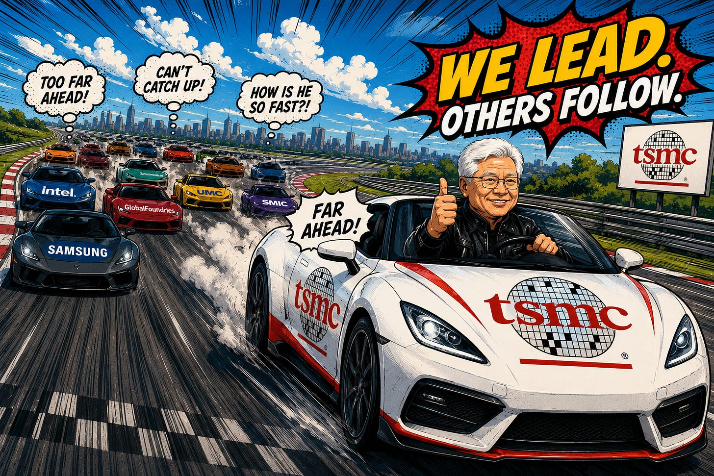
The AI semiconductor boom is no longer simply a contest to buy more GPUs. It is becoming a competition for access to advanced logic, HBM, packaging, interconnect, thermal engineering, power delivery—and, above all, manufacturing certainty.
TSMC’s June 2026 revenue matters for more than one reason.
At the most immediate level, it is an exceptionally strong data point ahead of the company’s second-quarter earnings call. TSMC reported consolidated revenue of NT$442.68 billion for June, up 6.2% from May and 67.9% from a year earlier. Revenue for the first six months of 2026 reached NT$2.404 trillion, an increase of 35.6% year over year.

Monthly revenue can be affected by shipment schedules, customer acceptance timing, product mix and currency movements. One record month should therefore not be treated as a complete forecast for the next several quarters.
Yet the scale of the increase is difficult to dismiss as accounting noise. It supports a broader conclusion: AI-related semiconductor demand remains strong enough to keep leading-edge wafer capacity, advanced packaging and associated supply chains operating under sustained pressure.
More importantly, it suggests that semiconductor pricing power is moving deeper into the manufacturing layer.
For most of the early AI investment cycle, the market framed the story as a shortage of GPUs. Cloud service providers wanted more accelerators; Nvidia and other chip designers wanted more wafers; investors therefore watched accelerator shipment volumes.
That explanation is no longer sufficient.
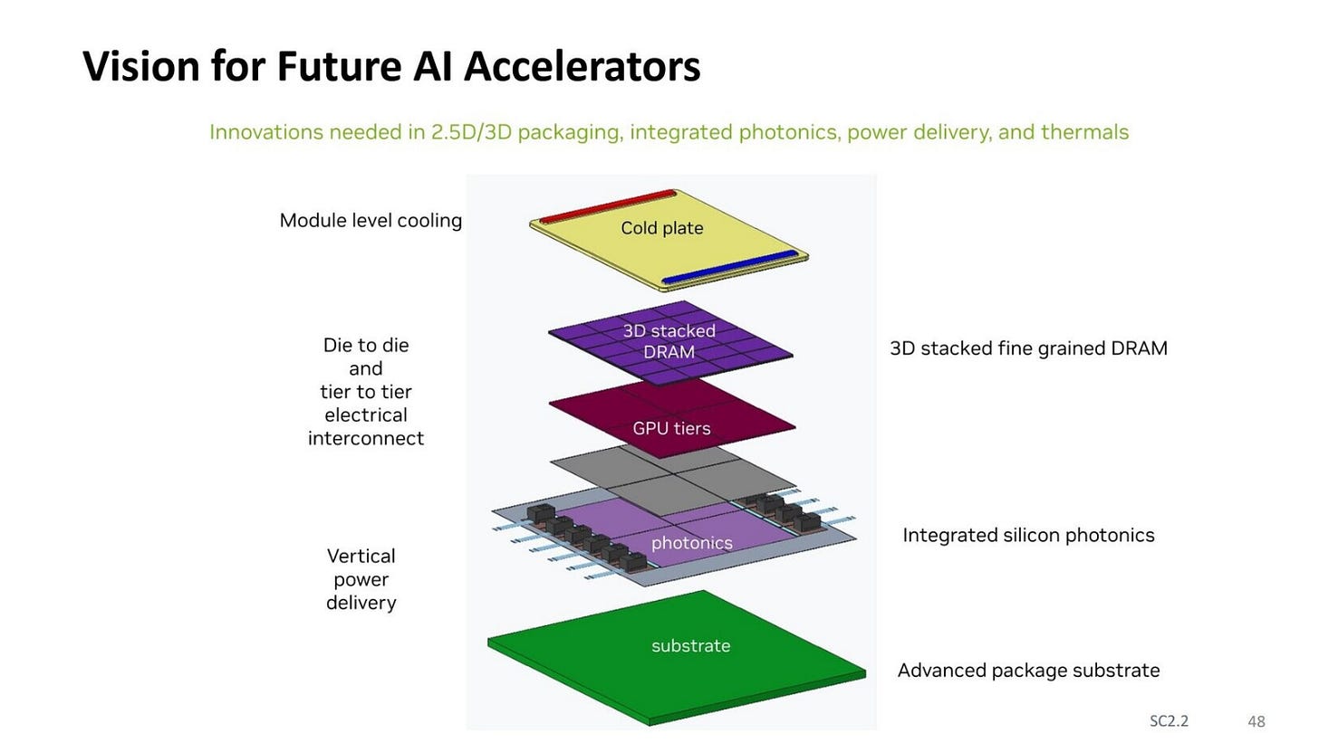
In 2026, the central bottleneck is not merely whether a company can design a competitive compute die. The real challenge is whether it can manufacture, package, power and cool an entire AI computing platform at scale. That platform may require leading-edge logic, HBM, advanced substrates, silicon interposers, high-speed chip-to-chip links, precision bonding, liquid cooling and megawatt-class data-centre power infrastructure.
The semiconductor industry has moved from a chip shortage to a system-integration shortage.
TSMC sits near the centre of that transition.

3月12日
Below we will share:
From GPU demand to manufacturing dependency
Why this pricing cycle is different
Advanced nodes remain critical—but …
Yield is becoming a system-level calculation
HBM confirms that the bottleneck is becoming systemic
Backside power and the next stage of AI silicon
Global investment is expanding—but …

3月5日

2025年11月29日
From GPU demand to manufacturing dependency
The strongest interpretation of TSMC’s June performance is not simply that customers ordered more wafers. It is that the largest AI companies have become increasingly dependent on a limited number of manufacturing flows.
Source: NVIDIA
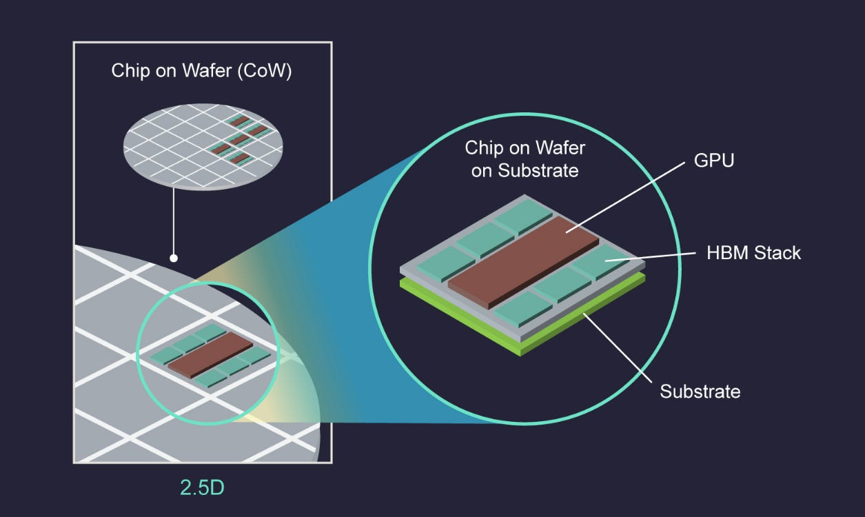
An advanced AI accelerator must pass through several interdependent stages. Its compute dies must be fabricated on a leading-edge process. HBM stacks must be produced, tested and matched with the package. The dies and memory must then be integrated through an interposer or redistribution structure. The final package must meet stringent requirements for warpage, mechanical stress, power integrity, signal integrity and thermal resistance.
A delay at any one of those stages can prevent the complete AI system from shipping.
This creates a different form of economic leverage. Customers are no longer purchasing only transistor density or wafer area. They are purchasing:
Access to qualified capacity;
Predictable yield;
Coordinated front-end and back-end production;
Packaging availability;
Faster time-to-ramp;
And confidence that several billion dollars of AI infrastructure can be deployed on schedule.
In other words, customers are paying for execution certainty.
The June revenue figure suggests that these conditions did not ease materially as the second quarter ended.
5月14日
Why this pricing cycle is different
Traditional foundry cycles are usually analysed through utilisation rates.
When consumer electronics demand weakens, fab utilisation falls, pricing becomes more competitive and foundries use discounts or incentives to protect volumes. When demand recovers and utilisation rises, those discounts narrow and selected products receive price increases.
The AI cycle is structurally different because scarcity is concentrated at the most technologically difficult points in the supply chain.
Leading-edge capacity cannot be created in a few months. TSMC has noted that constructing and ramping a new fab generally takes two to three years. Advanced packaging capacity also requires specialised equipment, process development, customer qualification and yield learning. Adding nominal floor space is not the same as adding qualified output.
As a result, foundry pricing power may not appear only as a visible increase in the quoted price of a wafer. It can also appear through a more favourable mix of advanced nodes, higher packaging content, reduced discounting, firmer capacity commitments and greater customer willingness to pay for accelerated qualification and dependable allocation.
The product being monetised is no longer just the wafer.
It is the complete manufacturing pathway.
This matters because an AI customer’s economic calculation is different from that of a consumer-chip customer. A smartphone vendor may resist a small increase in semiconductor cost because the increase must be absorbed across millions of price-sensitive devices. A hyperscale operator, by contrast, may tolerate a significantly higher chip or packaging cost when a delay would leave a multi-billion-dollar data centre underutilised.
When the opportunity cost of waiting becomes greater than the cost of the semiconductor, supplier bargaining power increases.
Advanced nodes remain critical—but packaging is becoming equally strategic
Leading-edge logic remains the foundation of TSMC’s position.
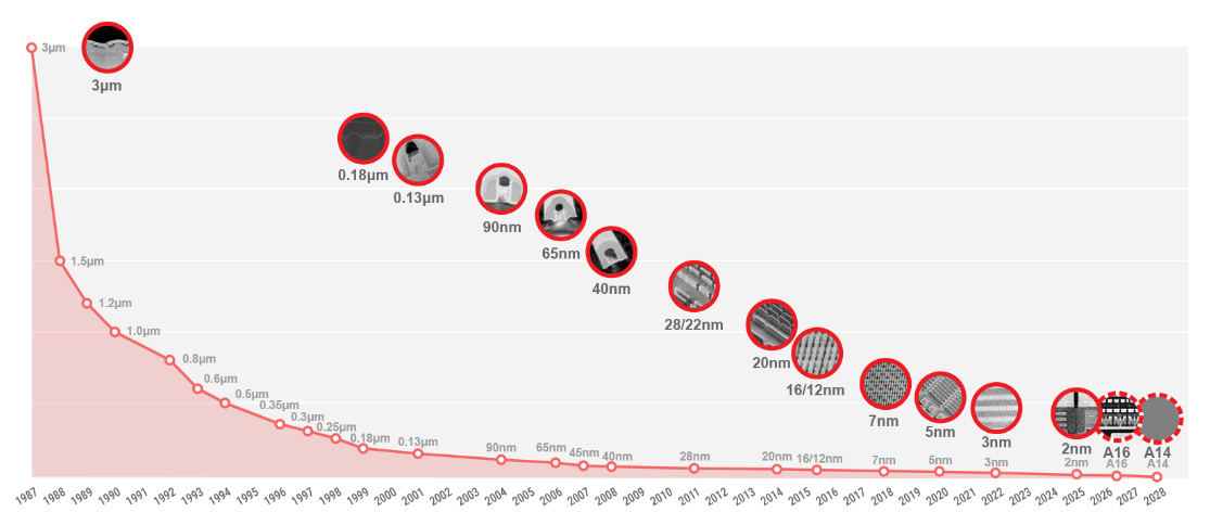
TSMC began high-volume manufacturing of N2 in the fourth quarter of 2025. The node introduces the company’s first-generation gate-all-around nanosheet transistor architecture and is ramping in Hsinchu and Kaohsiung for smartphone and HPC applications. TSMC is also adding N3 capacity in Taiwan, Arizona and Japan, partly because 3-nanometre technology is being used across AI accelerators, smartphones and HBM base dies.
Source: TSMC
The transition from FinFETs to nanosheet transistors improves electrostatic control and gives chip designers greater flexibility in balancing performance, leakage and cell architecture. TSMC says N2 can deliver approximately 10% to 15% higher speed at the same power, or 25% to 30% lower power at the same speed, compared with N3E.
For AI systems, however, transistor scaling alone is no longer enough.
The compute die is growing, but reticle limits constrain how large a monolithic die can become. Yield also declines as die area increases because a larger die has a greater probability of containing a fatal defect. Chiplets, 2.5D integration and 3D stacking therefore allow designers to assemble larger systems from multiple logic, I/O and memory dies.
That shifts more value into advanced packaging.
TSMC is already producing CoWoS packages measuring approximately 5.5 reticle sizes and plans to introduce a 14-reticle-size version in 2028. According to the company, that future configuration could integrate roughly ten large compute dies and twenty HBM stacks.
This is not a routine packaging roadmap. It represents a transition from packaging as the final assembly step to packaging as a primary system architecture.
At that scale, the engineering challenges become severe.
Larger interposers and packages are more vulnerable to warpage because silicon, organic substrates, underfills and moulding materials expand at different rates during heating and cooling. Mechanical stress can damage microbumps or produce delamination. Longer interconnect paths increase insertion loss and complicate signal timing. Higher current density intensifies voltage droop and electromigration risks. Concentrated heat from compute dies and HBM stacks increases the importance of thermal interface materials, heat spreaders and direct liquid cooling.
TSMC has acknowledged that larger AI packages must address mechanical stress, warpage and thermal limitations. It is developing larger CoWoS configurations while also working on SoIC 3D integration and a CoPoS pilot line for future panel-level packaging.
These technical difficulties strengthen the economic moat. Advanced packaging is difficult not because competitors cannot purchase equipment, but because high-volume integration requires accumulated process knowledge, materials engineering, design rules, simulation tools, customer co-development and years of yield learning.

7月13日
Yield is becoming a system-level calculation
The economics of an AI package depend on more than the yield of an individual wafer.
Source: LAM
Consider a simplified package containing several compute dies, multiple HBM stacks, an interposer and a large organic substrate. Every component must meet specifications, and every assembly step must succeed. Even when the yield of each individual component is high, the combined package yield can fall because the probabilities multiply.
This is why known-good-die testing, wafer-level inspection, microbump uniformity, hybrid-bonding quality and package-level burn-in are becoming increasingly important.
A defect discovered before integration may result in the loss of one die. A defect discovered after several expensive compute dies and HBM stacks have been assembled can result in the loss of an entire high-value package.
The foundry and packaging provider that can improve compound yield therefore creates value far beyond the cost of processing a wafer. It reduces material loss, shortens cycle time and improves the customer’s confidence in its product launch.
This is another reason the AI foundry pricing cycle may remain stronger than previous semiconductor upcycles. Customers may be willing to pay more for a manufacturing partner with higher effective system yield, even when another supplier offers a lower nominal wafer price.
HBM confirms that the bottleneck is becoming systemic
The memory market reinforces this interpretation.
Industry report expects conventional DRAM contract prices to increase by 13% to 18% quarter over quarter in the third quarter of 2026, while NAND Flash contract prices are projected to rise by 10% to 15%. The firm identified AI inference and large-scale data-centre deployment as major demand drivers, while also warning that consumer customers are approaching their affordability limits.
This creates an increasingly divided semiconductor market.
AI infrastructure can absorb higher component prices because the economic value of compute capacity remains high. PCs, smartphones and other consumer products have much less flexibility. As suppliers allocate more wafer capacity and capital expenditure toward HBM, server DRAM and enterprise storage, consumer customers must compete for the remaining output.
The pressure therefore spreads beyond HBM itself. It affects conventional DRAM, mobile memory, client SSDs and modules as production capacity and investment priorities move toward data centres.
The HBM4 transition adds another layer of technical complexity.
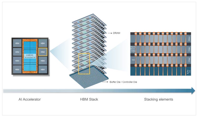
HBM4 doubles the interface width from 1,024 to 2,048 bits, significantly increasing the number of electrical connections between the memory stack and the logic platform. SK hynix says its HBM4 architecture provides more than 40% better power efficiency than the previous generation.
Industry report mentioned that SK hynix began mass-production shipments of 12-layer HBM4 to Nvidia at the end of June. Because the report has not been independently confirmed in a detailed customer announcement, it should be treated as a reported supply-chain development rather than a formally disclosed shipment schedule.

Nevertheless, the direction is clear. HBM4 is not simply faster DRAM. Its base die, interface, thermal behaviour and package integration must be co-optimised with the accelerator. The memory supplier, logic foundry, packaging provider and AI-chip designer must align their development schedules much earlier than in traditional server platforms.
The competitive unit is becoming the entire technology stack.

7月9日
Backside power and the next stage of AI silicon
Power delivery is also moving closer to the centre of process differentiation.
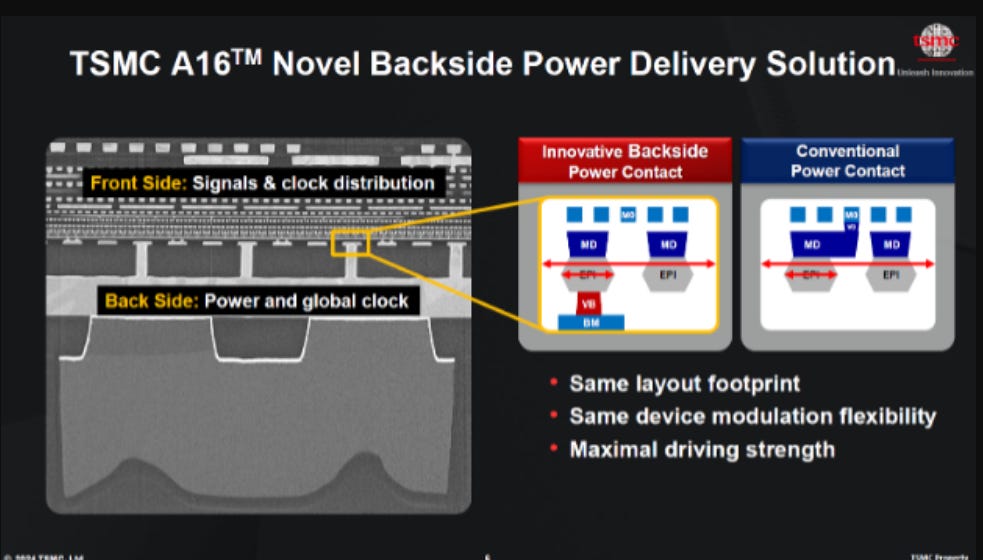
As transistor density rises, conventional front-side interconnect layers must carry both signal wires and power distribution. This creates routing congestion and increases resistance in the power-delivery network. Voltage loss becomes particularly problematic in large AI processors drawing enormous current at low operating voltages.
TSMC’s A16 technology combines nanosheet transistors with its Super Power Rail backside power-delivery architecture. By moving part of the power network to the rear of the wafer, the technology frees front-side routing resources for signals and can improve power integrity and logic density. TSMC currently targets A16 for mass production in 2027.
Source: TSMC
This is relevant to pricing because future process nodes are not merely smaller versions of current nodes. They are becoming integrated platforms combining transistor architecture, backside power, interconnect optimisation, design-technology co-optimisation and advanced packaging.
The cost and risk of developing such platforms are rising. At the same time, the number of suppliers capable of delivering them at high yield is narrowing.
That combination supports stronger long-term pricing discipline.
Global investment is expanding—but not necessarily loosening the bottleneck
The broader industry is responding with enormous capital commitments.

4月24日
Micron has increased its planned US investment to more than US$250 billion through 2035. The programme includes memory manufacturing in New York, Idaho and Virginia, as well as US$3 billion of additional semiconductor ecosystem investment. Micron also committed US$500 million to support GlobalWafers’ silicon-wafer facility in Texas and entered a ten-year supply arrangement.
These investments are large, but they do not imply an immediate end to scarcity.
New fabs require years to construct, equip, qualify and ramp. Memory capacity cannot be shifted frictionlessly between products, particularly when HBM requires additional wafer processing, TSV formation, stacking, bonding and testing. Advanced packaging expansion faces its own equipment, materials and workforce constraints.
Capital expenditure is rising because the industry expects structural demand. But the time required to convert capital into qualified output means pricing power can persist during the expansion phase.
Semiconductor fragmentation strengthens strategic suppliers
China’s localisation campaign adds a geopolitical dimension.
A survey cited by Bloomberg indicated that Chinese executives expected domestically produced accelerators to account for approximately 46% of their AI-chip budgets over the following twelve months, compared with about 30% at the time of the survey.
The percentages should not be interpreted as a precise forecast for the entire Chinese market. They nevertheless illustrate the direction of travel: the global semiconductor industry is dividing into increasingly distinct technology and supply ecosystems.
This fragmentation can create duplicate capacity in some areas while increasing scarcity in others. Companies may need separate chip designs, software stacks, manufacturing routes and supplier qualifications for different markets. Export controls may limit access to certain accelerators or production tools, while localisation mandates encourage earlier procurement commitments and longer-term domestic investment.
Paradoxically, a more fragmented semiconductor market can make the most indispensable suppliers even more valuable. Customers may have more strategic reasons to diversify, but fewer technically equivalent alternatives for their most advanced products.
The limits of the pricing-power thesis
The argument should not be taken too far.
TSMC is not immune to cyclicality. AI customers could over-order, cloud capital expenditure could slow, or improvements in model efficiency could reduce the amount of hardware required for specific workloads. Competitors could gain share in selected foundry or packaging technologies. Additional CoWoS capacity could eventually reduce urgency and shorten lead times.
Higher revenue also does not automatically translate into proportionally higher margins.
Overseas expansion is expensive. TSMC has estimated that the ramp of international fabs could dilute gross margin by approximately two to three percentage points in the early stages, widening to three to four points later. The company must also absorb higher depreciation, labour, energy and supply-chain costs as it builds a more geographically distributed manufacturing network.

3月3日
Advanced packaging itself can become a margin challenge if customers demand larger packages and more complex integration faster than yields improve. A package containing more dies and HBM stacks carries more revenue, but it also carries greater material exposure and a higher cost of failure.
The central issue is therefore not whether TSMC can raise prices indefinitely. It is whether its technology differentiation and manufacturing leverage can offset the rising cost of supporting the AI ecosystem.
So far, the June revenue figure suggests that the balance remains favourable.
Three indicators to watch next
The first signal will be TSMC’s second-quarter earnings call on July 16. Investors should focus less on the retrospective June number and more on second-half revenue guidance, gross-margin resilience, N3 and N2 utilisation, advanced packaging expansion and customer visibility
The second will be ASML’s second-quarter results on July 15. ASML raised its 2026 revenue outlook after reporting €8.8 billion of first-quarter sales. Its order commentary will reveal whether leading-edge foundries and memory manufacturers are still accelerating EUV investment or beginning to moderate their expansion plans.
The third will be the spread of long-term supply agreements across HBM, wafers, substrates, advanced packaging materials and manufacturing equipment. The more frequently customers commit capital and volume years in advance, the stronger the evidence that the industry is moving from a temporary shortage into a structurally tighter production model.
3月20日
The next AI cycle will be priced at the manufacturing layer
TSMC’s record June revenue should not be viewed only as another strong monthly sales figure.
It is evidence that the centre of gravity in the AI semiconductor industry is changing.
The first phase of the AI boom rewarded companies that controlled accelerator architecture. The next phase will increasingly reward companies that control the physical ability to turn those architectures into manufacturable systems.
That means leading-edge transistors, but also HBM base dies, interposers, hybrid bonding, large-format CoWoS, backside power delivery, warpage control, thermal management, testing and coordinated capacity planning.
AI has not eliminated semiconductor cyclicality. It has concentrated demand around a small number of extraordinarily difficult manufacturing technologies.
When customers are competing not merely for chips but for the certainty that their AI platforms can be delivered, installed and scaled on time, the supplier controlling the manufacturing bottleneck gains more than volume.
It gains strategic pricing power.
TSMC’s June revenue suggests that the next semiconductor pricing cycle has already begun—and that it will be driven not simply by how many wafers the industry can produce, but by how few companies can reliably assemble the complete AI system.

2025年9月25日

2025年6月27日


PreviousNext