Intel’s CPO Packaging Roadmap: From Glass Couplers to Pluggable Optical Connectors
Intel’s CPO Packaging Roadmap: From Glass Couplers to Pluggable Optical Connectors
- Source: SemiVision
- Author: SEMIVISION
- Published: 2026-07-03T11:48:05+08:00
- URL: https://tspasemiconductor.substack.com/p/intels-cpo-packaging-roadmap-from (5) Intel’s CPO Packaging Roadmap: From Glass Couplers to Pluggable Optical Connectors


Intel’s CPO Packaging Roadmap: From Glass Couplers to Pluggable Optical Connectors
Original Article By SemiVision Research [Reading time: 18 mins]

Jul 03, 2026
∙ Paid

Over five days, DAC provides over 300 technical presentations and sessions that are selected by a committee of electronic design and university research experts offering information on recent developments and trends, management practices and new products, methodologies, and technologies in the electronics industry.
The conference is sponsored by the Association for Computing Machinery (ACM) and the Institute of Electrical and Electronics Engineers (IEEE), and is supported by ACM’s Special Interest Group on Design Automation (SIGDA) and IEEE’s Council on Electronic Design Automation (CEDA).
From Glass Couplers to Pluggable Optical Connectors: A Review of Two Intel Papers on CPO Optical Coupling Packaging Technology
Co-packaged optics, or CPO, is becoming an important technology direction for AI data centers and high-performance computing systems. As the scale-up network bandwidth of GPU clusters and AI accelerators continues to increase, traditional copper interconnects are gradually reaching limits in reach, power consumption, and density. As a result, the industry is pushing optical I/O closer to the chip package.
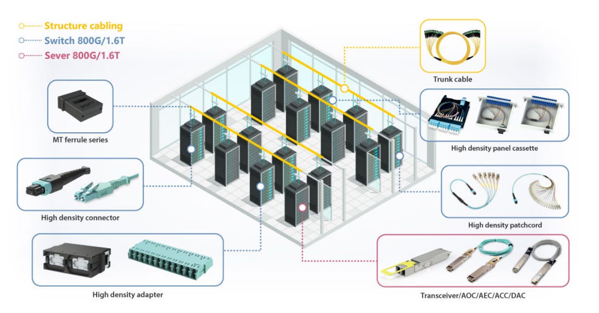
Data Center Connectivity and Cabling Solutions / aconoptics.com
This article reviews two Intel-related ECTC 2026 papers: “V-groove Based Edge Coupling Enabled by Optical Glass Coupler Attach for Co-packaged Optics” and “Multi-channel and multi-scale Optical Performance for a Detachable Edge-Coupling Connector with a Glass Coupler and Expanded Beam in CPO.”
The first paper focuses on the passive alignment and attachment process between a glass coupler and the PIC V-groove, including material selection, dimensional metrology, and reliability. The second paper further integrates the glass coupler with an expanded-beam detachable connector, establishing multi-scale optical simulation, multi-channel Monte Carlo analysis, and measured insertion-loss testing.
Taken together, the two papers reveal the core challenge of CPO optical coupling packaging: it is not simply about connecting fiber to a silicon photonics chip. The real task is to build an optical-electrical packaging architecture that is manufacturable, testable, repairable, low-loss, and reliable.

2025年6月25日

2025年6月3日
Research Background: Why CPO Needs a New Optical Coupling Package
Network connectivity in AI data centers can be roughly divided into scale-out and scale-up. Scale-out usually connects different servers or racks, where optical communication is already widely used. Scale-up, by contrast, provides extremely high-bandwidth and low-latency interconnects within a single rack or between adjacent accelerators. Historically, this domain has relied heavily on high-speed SerDes and copper interconnects.
As 200 Gbps SerDes over copper backplane begins to be deployed, electrical interconnects may still extend for some time. However, they will eventually face limitations in reach, power, and density.
The basic idea of CPO is to move the electrical-to-optical, or E/O, conversion module closer to the switch ASIC, GPU, XPU, or accelerator package, and in some cases even integrate it deeper inside the package. This shortens the high-power electrical channel, reduces I/O PHY complexity and power consumption, and increases bandwidth density around the package edge or chip perimeter.
However, CPO also introduces a major packaging challenge: how does light enter and exit the package?
The waveguide mode size on a silicon photonics PIC is very small, while the mode field diameter of an optical fiber is relatively large. If a traditional fiber array unit, or FAU, is directly attached to the PIC V-groove, it may provide low optical loss, but it also sacrifices repairability, assembly flexibility, and yield management.
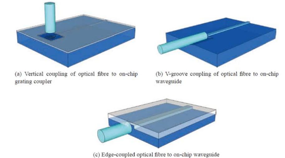
If CPO is to become a high-volume manufacturing technology, it needs an optical interface that can deliver low-loss coupling while also supporting pluggability, testing, and replacement.
These two papers are essentially answering that question. Paper 19 first establishes the fundamental process for attaching a glass coupler to a PIC. Paper 12 then connects this glass coupler to an expanded-beam connector, forming a more complete detachable edge-coupling CPO architecture.

2025年6月10日
Below we will share:
Review of Paper 19: V-groove and Glass Coupler Attachment Process
Materials and Epoxy Design
Passive Alignment Attachment Process and Dimensional Metrology
Process Optimization: Bonding Force and Epoxy Shrinkage
Review of Paper 12: Detachable Expanded-Beam Connector and Multi-scale Analysis
Why Expanded Beam Matters
Integrated Interpretation: From Process Unit to System Architecture

2025年5月28日
Review of Paper 19: V-groove and Glass Coupler Attachment Process

The core of “V-groove Based Edge Coupling Enabled by Optical Glass Coupler Attach for Co-packaged Optics” is the use of a rigid glass coupler to replace traditional direct fiber attach, serving as an intermediate interface between the PIC and the external optical connector.
The PIC used in the paper is a full-thickness silicon PIC originally designed for direct fiber attach. It has 24 channels with a 250 µm pitch and uses a metamaterial-based spot size converter, or SSC, for mode conversion. Compared with grating coupling, edge coupling offers advantages such as broad bandwidth and low loss, but it also requires extremely precise optical alignment. In addition, the thin-film structure of the SSC is relatively fragile and is sensitive to epoxy materials and assembly thermal history.
The role of the glass coupler is to convert the PIC-side V-groove and SSC interface into a structure that can later connect with an external connector or fiber array. The paper notes that glass materials offer low optical loss, high mechanical stability, and a coefficient of thermal expansion that can be matched with silicon. The waveguide propagation loss is approximately 0.2 dB/cm for a single path, comparable to polymer waveguides.

To match the PIC interface, the glass coupler is fabricated with cylindrical protrusions of 127 µm diameter arranged at a 250 µm pitch. Functionally, these protrusions act like inverse V-grooves, allowing the coupler to be passively aligned to the PIC V-groove.
There is an important design difference here. A traditional fiber array is relatively flexible, and each fiber has some degree of adjustability. A rigid glass coupler, by contrast, is an integrated rigid structure, and the relative position of each channel is defined by the fabrication process. This gives it advantages in dimensional stability and modeling, but it also means that any overall tilt, warpage, or dimensional error can affect multiple channels simultaneously.
For this reason, the paper places strong emphasis on dimensional metrology and attach process control.
Materials and Epoxy Design
The paper does not use a single epoxy to solve all requirements. Instead, it separates the functions of mechanical epoxy, or ME, and optical epoxy, or OE.
ME is mainly used in the V-groove region to provide mechanical fixation. It first undergoes UV snap cure, followed by a subsequent thermal cure. OE is a low-viscosity and low-modulus material used to fill the undercut below the SSC, preventing an air gap between the PIC and the coupler while reducing damage to the fragile SSC membrane.

This material design reflects a typical challenge in CPO packaging: the material must simultaneously satisfy mechanical fixation, optical transparency or refractive-index requirements, thermal reliability, flow control, and process compatibility.
The paper specifically mentions that if the ME gap is not well controlled, OE may leak out, causing optical performance degradation and even contamination of downstream tools and package surfaces. If ME flows underneath the SSC, it may damage the SSC membrane during thermal processing. This shows that CPO optical packaging is not simply about “gluing components together.” It is a highly precise material and fluid-control problem.
2025年5月27日
Passive Alignment Attachment Process and Dimensional Metrology
This study adopts vision-based passive alignment without optical feedback. In other words, the assembly process does not rely on real-time optical power maximization. Instead, attachment is completed through mechanical features on the PIC and glass coupler, combined with high-precision vision positioning.
This approach is attractive for mass production because active optical alignment is usually slower and more expensive. However, whether passive alignment can succeed depends on component dimensional accuracy, tool flatness, bonding force, and material shrinkage control.
The paper establishes a metrology method for measuring the coupler relative to the PIC reference plane, observing roll, pitch, flatness, and height variations across different zones. The value of this kind of metrology is that it allows engineers to correlate optical insertion loss with mechanical dimensional deviations. If certain edge channels show worse insertion loss, engineers can trace whether the root cause comes from coupler tilt, warpage, or epoxy shrinkage.
Optical Insertion Loss Measurement
The paper uses a contact-free, non-invasive optical probe system to measure insertion loss, or IL. The system includes a six-degree-of-freedom stage and can use high-speed active alignment to find the best coupling position, with resolution down to the nanometer scale.

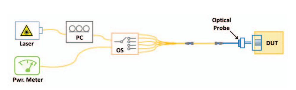
Diagram of optical IL metrology test structure for optical IL data collection.
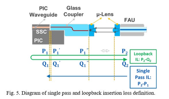
The test setup uses a 1310 nm laser source, polarization controller, optical switch, and power meter. IL across different channels is measured through loopback channels.
In a half-day repeatability test, 15 units across multiple loopback channels showed an optical IL repeatability standard deviation of less than 0.1 dB. This is important for process development. If the measurement system itself has too much variation, engineers cannot determine whether IL changes come from the process, materials, reliability stress, or the measurement system.
Process Optimization: Bonding Force and Epoxy Shrinkage
Bonding force is one of the most critical process parameters in this paper. If the force is too low, the coupler cannot overcome friction and complete self-alignment inside the V-groove. If the force is too high, the thin glass coupler may warp, and the bond head may deflect, resulting in misalignment and optical degradation.
The paper shows that under high bonding-force conditions, the IL of edge loopbacks may be 2–3 dB higher. This means force-induced deformation can directly translate into optical performance degradation.
The cure shrinkage of the ME material can also cause warpage. The paper compares different mechanical epoxies and shows that low-shrinkage materials can reduce the glass warpage amplitude by about half. In addition, after optimizing both the material and the subsequent flip-chip bonding thermal process, ME delamination was reduced, and inline IL degradation improved by more than 0.5 dB.

Reliability Results
The paper tested three types of reliability stress: Thermal Cycling condition G, or -40°C to 125°C for 450 cycles; High Temperature Storage at 150°C for 500 hours; and uHAST at 110°C and 85% RH for 275 hours.
The results show that after TCG, the one-way IL increase for all channels was less than 0.7 dB per direction. HTS also had a relatively limited impact, with all measured channels remaining within 0.6 dB after 500 hours. uHAST caused more noticeable degradation, but most units still maintained per-channel IL degradation within 1 dB after 275 hours.
These results suggest that the glass-coupler attachment scheme has preliminary reliability feasibility. However, humid and high-temperature environments remain an area that requires further optimization. For CPO, this is reasonable. Optical interfaces are highly sensitive to small deformation, moisture absorption, interface delamination, and refractive-index changes, and uHAST often amplifies these issues.
Review of Paper 12: Detachable Expanded-Beam Connector and Multi-scale Analysis

“Multi-channel and multi-scale Optical Performance for a Detachable Edge-Coupling Connector with a Glass Coupler and Expanded Beam in CPO” can be viewed as an extension of Paper 19.
Paper 19 mainly answers the question: how can a glass coupler be stably attached to a PIC?
Paper 12 goes further and asks: if we want the CPO optical interface to be pluggable, serviceable, and suitable for high-volume manufacturing, how should the full optical path be designed, simulated, and verified?
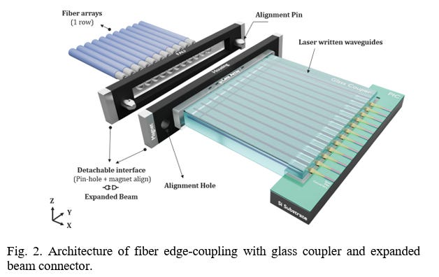
The architecture proposed in the paper consists of a fan-out glass coupler and an expanded-beam connector. The glass coupler contains 3D waveguides that can perform port mapping, convert mode field diameter, and interface with the PIC SSC. It can also transform the high-density channel arrangement at the PIC facet into a format that is easier to handle at the connector or fiber-array side.
The connector provides a detachable interface. Through a lens array, the optical beam is expanded and approximately collimated, relaxing the alignment tolerance of the pluggable interface.

Why Expanded Beam Matters
Traditional fiber pigtails permanently attached to the PIC are not ideal for field serviceability or package yield. If the fiber or connector has issues during downstream assembly or system maintenance, the entire package may be difficult to repair.
The concept of a detachable expanded-beam connector is to make the most sensitive PIC-coupler interface a high-precision permanent attachment, while using an expanded beam to relax alignment tolerance at the external pluggable interface.
The basic intuition behind expanded beam is simple: when the beam diameter becomes larger, it is less sensitive to small lateral offsets or angular deviations.
The connector in the paper uses metal alignment pins to align the lens array and magnets to provide retention force, allowing the operator to manually plug and unplug the connector. The design goal is not merely the lowest possible single-event loss. Instead, it balances low loss, repeatable plug-unplug behavior, repairability, and manufacturability.
Multi-scale Optical Modeling
The most academically valuable part of this paper is the establishment of a multi-scale optical analysis methodology.
A CPO optical path involves different physical scales and behaviors at the same time. The waveguides and SSC inside the PIC are guided-wave problems at the nanometer-to-micrometer scale. The glass waveguide and micro-lens are micro-scale structures. The expanded-beam connector interface includes millimeter-scale free-space propagation.
Therefore, the paper does not use a single simulation tool to handle all regions. Instead, it selects different methods according to physical scale.
Fiber and glass waveguides are analyzed using eigenmode analysis to obtain mode profile, propagation loss, and bending loss. The PIC-side edge inverted taper and SSC are simulated using the eigenmode propagation method to analyze mode conversion. Free-space regions such as lens-to-lens or lens-to-waveguide are analyzed using physical optics propagation, or POP, to model diffraction and beam shaping.
This segmented modeling approach balances accuracy and computational efficiency.
This is highly important in engineering practice. If the entire structure is simulated using full-wave 3D simulation, the computational cost may be prohibitive. If the entire system is modeled using simplified Gaussian optics, important details such as SSC behavior, waveguide mode mismatch, and lens-interface effects may be ignored. A multi-scale workflow allows designers to predict the complete optical path loss within a reasonable time.

Multi-channel Monte Carlo Analysis
Another key point is multi-channel Monte Carlo analysis. Optical coupling loss is highly sensitive to micron-level alignment errors. In high-volume manufacturing, the most important metric is not nominal design loss, but the yield under statistical distribution.
The paper emphasizes that looking only at a single channel or a contact channel may be overly optimistic. Looking only at edge channels may also misrepresent the true worst channel.
Taking the PIC-to-glass coupler interface as an example, variations in coupler cylindrical protrusion radius, PIC V-groove opening width, coupler height, and array tilt can jointly affect loss. Some variations affect only a single channel, while others cause tilt across the entire rigid array, changing the relative positions of all channels.
After comparing different calculation methods, the paper points out that the most rigorous approach is to dynamically calculate the self-variation and cross-channel variation of all 24 channels in each Monte Carlo DOE, identify the worst channel under that specific condition, and then use these worst-channel results to build a unit-level loss-yield curve.
This method is crucial for mass-production design. Whether a CPO module passes qualification usually depends on the worst channel in the entire unit, not the average channel. If just one channel has excessive loss, the link budget of the entire optical engine may be compromised.
Measured Results and Reliable Plug-Unplug Operation
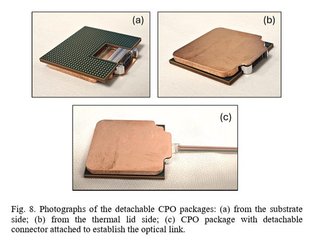
Paper 12 fabricated package samples with a detachable edge-coupling connector. The assembly process first active-aligns the connector to the glass coupler, then attaches the assembled unit to the PIC. Optical module packaging and thermal lid installation are then completed.
The paper emphasizes that the connector’s compact form factor can fit under the heat spreader. This is important for CPO system integration because the optical connector must not interfere with the thermal structure.
Optical testing used a 1310 nm laser source, polarization controller, optical switch, and power meter. The measured fiber-to-PIC single-direction coupling loss was approximately -1.55 dB, which the paper considers competitive for a detachable architecture.
More importantly, plug-unplug variation was far below 0.01 dB. During a live demonstration at Supercomputing Conference 2025, the connector underwent more than 100 plug-unplug cycles while still showing minimal performance variation and no part failure.
This result is meaningful for CPO. Low IL provides margin for the link budget. Low plug-unplug variation supports system repairability and field operation. A detachable connector means the package does not have to be permanently tied to fiber, which helps testing, yield management, logistics, and customer use.
Integrated Interpretation: From Process Unit to System Architecture
These two papers can be viewed as two levels of the same technology roadmap.
Paper 19 establishes the foundation at the process-unit level: how should the glass coupler be attached to the PIC? Is passive alignment feasible? How should epoxy be selected? What is the relationship between bonding force, warpage, delamination, and IL? Does optical performance remain stable after reliability stress?
If these questions are not solved, even the most elegant connector architecture cannot be implemented.
Paper 12 establishes the methodology at the system optical-path level: how can the glass coupler be connected to a detachable expanded-beam connector? How should the optical path be simulated when it spans waveguides, lenses, free space, and PIC SSC structures? How should the worst-case loss of a multi-channel rigid array be evaluated using Monte Carlo analysis? Can the pluggable interface maintain repeatability under low-loss conditions?
Taken together, the two papers reveal four core technical requirements for CPO optical coupling packaging.
The first is low loss. The CPO optical path passes through multiple interfaces, including the PIC SSC, glass waveguide, lens, connector, and fiber. Each interface consumes part of the link budget. The roughly -1.55 dB single-direction coupling loss reported in Paper 12 indicates that an expanded-beam detachable architecture has the potential to maintain acceptable loss.
The second is high alignment tolerance. PIC edge coupling is inherently sensitive to alignment. The value of an expanded-beam connector is that it relaxes alignment requirements at the pluggable interface, while the PIC-coupler side is managed through high-precision passive alignment and a rigid glass structure.
The third is manufacturability and testability. Permanent fiber pigtails make packaging, testing, and handling more difficult. A detachable connector allows the optical path to be accessed at different stages and supports electrical and optical validation before final assembly, helping reduce cost and improve yield.
The fourth is reliability. CPO packages must endure thermal cycling, high-temperature storage, humid heat, plug-unplug cycles, heat-spreader assembly, and system operation. The TCG, HTS, and uHAST results in Paper 19, together with the plug-unplug stability in Paper 12, suggest that this technology path is moving closer to practical deployment.
Implications for the CPO Industry
From an industry perspective, the value of these two papers is not limited to a single connector or glass coupler. More importantly, they demonstrate the engineering mindset required to commercialize CPO.
First, CPO cannot rely only on silicon photonics chip design. PIC waveguides and modulators are important, but once the technology moves into real systems, optical coupling, connectors, packaging materials, thermal structures, testing flows, and reliability become the key factors determining whether a product can enter mass production. These two papers focus on optical packaging around the PIC, which is a highly practical direction.
Second, CPO packaging requires mechanical-optical co-design. Traditional electronic packaging focuses on solder joints, RDL, underfill, warpage, and CTE mismatch. CPO adds a highly sensitive optical loss metric. A few microns of height difference, tilt, or epoxy shrinkage can turn into dB-level IL variation. Future optoelectronic packaging engineers will need to understand mechanical dimensions, material behavior, and optical mode coupling at the same time.
Third, pluggability will be one of the key conditions for CPO adoption in data centers. Data center systems require serviceability, replaceability, testability, and scalability. If fiber is permanently fixed to the package, handling, assembly, and maintenance risks increase. The low plug-unplug variation of the detachable expanded-beam connector directly addresses this system-level problem.
Fourth, statistical design will matter more than nominal design. The multi-channel Monte Carlo analysis in Paper 12 shows that optical coupling interfaces cannot be evaluated only by ideal-condition loss. In mass production, engineers must understand how dimensional tolerances map to unit-level yield and design specifications with a worst-channel mindset. This is similar to bump yield, warpage window, and RDL defect-density considerations in advanced packaging, except that the failure metric here becomes optical loss.
Future Research Directions
The two papers also point to several future research directions worth watching.
The first is vertical coupling and higher-density coupling architectures. The conclusion of Paper 19 mentions that these glass-attach learnings can be applied to next-generation vertical coupling with expanded beam. Compared with edge coupling, vertical coupling may reduce PIC shoreline limitations and provide more layout freedom for optical I/O inside the package.
The second is active optical link and bit-error-rate demonstration. Paper 12 notes that future work will include active link and BER demonstrations. This is critical because low IL and stable plug-unplug behavior are only the foundation of the optical channel. Ultimately, the technology still needs to prove that it can maintain data transmission quality under high-speed modulation, temperature variation, and system noise.
The third is the use of machine learning for design-rule optimization and packaging design-kit acceleration. CPO packaging has many variables, including lens design, waveguide geometry, coupler tolerance, epoxy flow, warpage, and connector repeatability. With enough simulation and measurement data, machine learning could help quickly explore the design window.
The fourth is end-to-end electrical-optical co-simulation. The ultimate value of CPO comes from reducing system power consumption and increasing bandwidth. Future evaluation will need to place the electrical channel, optical link, E/O conversion, thermal design, and advanced packaging into a unified model.

2025年3月28日
Conclusion
These two Intel-related papers jointly describe the development path of CPO optical coupling packaging from fundamental process technology to system architecture.
Paper 19 demonstrates that a glass coupler can be attached to a PIC through V-groove passive alignment, and it establishes process feasibility through material selection, bonding-force optimization, dimensional metrology, and reliability validation.
Paper 12 further integrates the glass coupler with an expanded-beam detachable connector. Through multi-scale optical modeling, multi-channel Monte Carlo analysis, and measured IL and plug-unplug stability, it demonstrates the possibility of a serviceable and manufacturable CPO optical interface.
The most important takeaway is that the success of CPO depends not only on silicon photonics devices, but also on whether optical packaging can simultaneously satisfy low loss, high density, pluggability, testability, reliability, and manufacturability.
The combination of glass couplers and expanded-beam connectors is a key route for pushing laboratory-stage silicon photonics technology into real data center systems.

2025年11月29日
2025年3月28日
Thanks for reading SEMIVISION @_@! This post is public so feel free to share it.


Previous