ECTC 2026: The Three HBM Battlegrounds Defining the Next AI Hardware Race
ECTC 2026: The Three HBM Battlegrounds Defining the Next AI Hardware Race
- Source: SemiVision
- Author: SEMIVISION
- Published: 2026-07-01T11:19:43+08:00
- URL: https://tspasemiconductor.substack.com/p/ectc-2026-the-three-hbm-battlegrounds (1) ECTC 2026: The Three HBM Battlegrounds Defining the Next AI Hardware Race


ECTC 2026: The Three HBM Battlegrounds Defining the Next AI Hardware Race
Original Article By SemiVision Research [Reading time: 19 mins]

Jul 01, 2026
∙ Paid

The Open Compute Project (OCP) is bringing together APAC communities for a very special two-day, in-person Summit to explore the many challenges and opportunities facing data center infrastructure, today and tomorrow. The OCP APAC Summit will showcase the latest innovations and technical advancements from around the world, and feature talks from experts who are researching, designing, building and running the next generation of hyperscale data center facilities and infrastructure. The Expo Hall will bring together buyers and sellers from the entire ecosystem and supply chain.
https://www.opencompute.org/summit/2026-ocp-apac-summit
The Three Key Battlegrounds in HBM Technology: High-Speed Interconnect, Vertical Power Delivery, and System-Level Thermal Management
In recent years, the performance bottleneck in AI and high-performance computing has no longer been defined only by how fast chips can compute. The more decisive question is whether data can move between processors and memory at sufficiently high bandwidth, low latency, and low power. This is exactly why HBM, or High Bandwidth Memory, has become one of the most critical components in advanced packaging.

Historical HBM total bandwidth scaling trend / Intel
HBM vertically stacks multiple DRAM dies using TSVs, then places the memory much closer to GPUs, ASICs, or XPUs through 2.5D and 3D packaging. The goal is simple: make the data path wider, shorter, and more energy-efficient.
But the next stage of HBM development is not just about stacking more DRAM layers or increasing signal speed. Several ECTC 2026 papers suggest that HBM is entering three simultaneous battlegrounds: high-speed package interconnect for HBM4E-class interfaces, more complex power delivery in 3D heterogeneous integration, and system-level thermal management under rising power density.
Together, these three areas will determine whether future AI and HPC packages can continue to scale.
Why HBM Has Become So Important
Traditional DRAM, connected to processors through DIMMs or conventional packages, faces longer data paths, higher I/O power, and limited bandwidth density. As AI models become larger, matrix operations increase, and data movement demand explodes, memory bandwidth often becomes the system bottleneck before raw compute does.
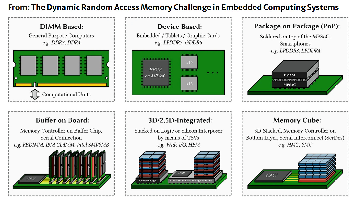
Source: The Dynamic Random Access Memory Challenge in Embedded Computing Systems
The core advantage of HBM is that it stacks multiple DRAM dies vertically and uses massive parallel I/O with short-distance interconnects to provide high bandwidth and lower energy per bit.
From HBM2, HBM2E, HBM3, and HBM3E to HBM4 and HBM4E, the development direction has been clear: higher per-pin data rates, more I/Os, more stacked DRAM layers, higher stack capacity, and shorter distance to the logic die.

These improvements are critical for AI GPUs and HPC accelerators because they need to read and write enormous volumes of weights, activations, KV cache data, and scientific computing datasets within extremely short time windows.
But higher HBM bandwidth is not free.
More I/Os mean denser package routing. Higher data rates make signal integrity harder. More stacks increase the difficulty of power delivery and thermal management. Larger packages create more challenges in warpage control, reliability, and yield.
Therefore, the next stage of HBM development is not only a memory design problem. It is a system engineering problem.
Below we will share:
Intel: EMIB-T: Enabling High-Speed Interconnect for 12+ Gb/s HBM4E
KAIST: 3D-HI-HBM: Power Delivery Becomes a Three-Dimensional Problem
Samsung: HCB HBM: Interconnect Becomes Part of the Thermal Path
Implications for the Semiconductor Supply Chain
AMD: HBM Shortages Are Pushing Vendors Toward LPDDR Alternatives

6月18日
EMIB-T: Enabling High-Speed Interconnect for 12+ Gb/s HBM4E

The first paper is Intel’s “Enabling 12+Gb/s HBM4E with EMIB-T Advanced Packaging Technology.”
The main message is clear: once HBM4E moves beyond 12 Gb/s, conventional package interconnect may no longer be sufficient to support both signal and power requirements. A more advanced bridge architecture is needed to co-optimize SI, or signal integrity, and PI, or power integrity.
The HBM4 and HBM4E challenge can be understood through two numbers.
The first is data rate. The paper focuses on HBM4E operation above 12 Gb/s.
The second is I/O count. The HBM4 generation is expected to expand from roughly 1K I/O to around 2K I/O. This means a single HBM stack could move toward 2 TB/s or even 2.5 TB/s of bandwidth.
For the system, this is attractive because memory bandwidth increases significantly. But for the package, it means routing density, crosstalk, insertion loss, IR drop, and PDN impedance are all pushed higher at the same time.
A traditional silicon interposer can provide strong routing density and electrical performance, but it is expensive and limited by reticle size. As ultra-large die complexes integrate multiple HBM stacks and large logic dies, the cost and manufacturing burden of full silicon interposers become increasingly heavy.
EMIB takes a different approach. Instead of using a full silicon interposer, it places localized silicon bridges only where high-density die-to-die interconnect is needed. This improves cost and area efficiency and makes large advanced packages easier to scale.
But traditional EMIB also has limitations. The bridge has limited metal layer count and lacks a direct vertical power delivery path. Power still mainly comes laterally through the package substrate. When HBM4E requires higher I/O density and lower-noise power delivery, this architecture can face higher IR drop, uneven micro-bump current distribution, and increased PDN impedance.
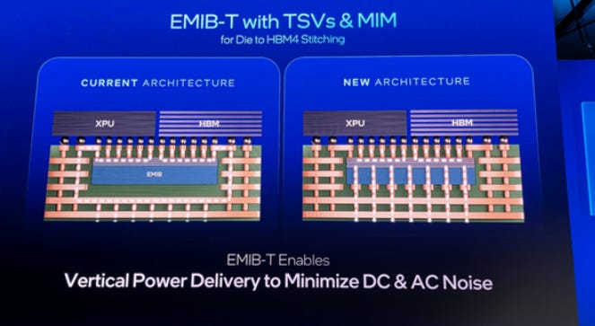
EMIB-T improves this by integrating TSVs, additional metal layers, and embedded decoupling capacitors into the bridge.
TSVs allow power to be delivered more directly and vertically into critical regions, reducing the burden on lateral power delivery. Additional metal layers provide more routing flexibility and help maintain controlled routing density under 2K I/O HBM4E requirements. MIM decaps provide high-frequency decoupling closer to the load, reducing PDN AC impedance.
The importance of this paper is not simply that it demonstrates the feasibility of 12+ Gb/s HBM4E. More importantly, it shows that HBM package design must now treat signal and power as one integrated problem.
In high-speed interfaces, signal traces cannot be evaluated only by insertion loss. Designers must also consider whether the return path is continuous, whether the reference plane is stable, whether coupling between adjacent lines is manageable, and whether power noise will become timing jitter or eye-margin loss.
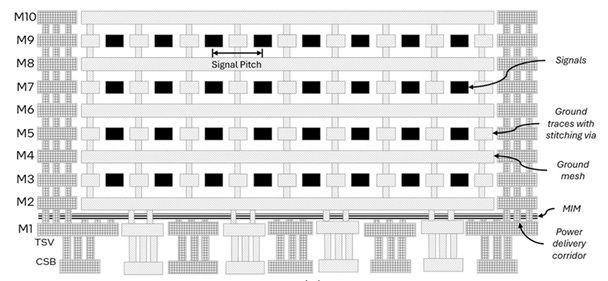
Representative EMIB-T stack-up with signals, ground, power mesh and metal–insulator–metal (MIM) layers.
According to the paper, the EMIB-T package improves PDN AC impedance by more than 82% compared with traditional EMIB without bridge-level MIM capacitors. This number shows that in-package power decoupling is no longer a secondary feature. It has become a core requirement for stable high-speed HBM channel operation.
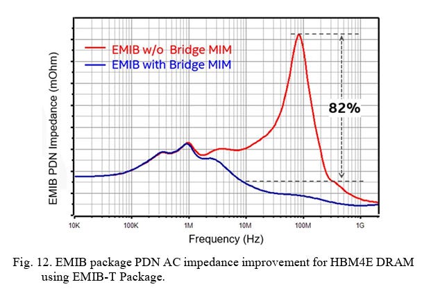
Another important point is the positioning of EMIB-T. It attempts to find a balance between the high performance of full silicon interposers and the cost flexibility of organic or RDL-based solutions.
For AI and HPC packaging, future package sizes will become larger, die counts will increase, and the number of HBM stacks may continue to grow. If every design depends on a large silicon interposer, cost and size constraints will become more severe. Localized bridge architectures with vertical power delivery, such as EMIB-T, may become an important path for large-scale heterogeneous integration.

2025年5月1日
3D-HI-HBM: Power Delivery Becomes a Three-Dimensional Problem
The second paper is KAIST’s“Power Distribution Network Design and Analysis for Multi-Stack 3D Heterogeneous Integrated High Bandwidth Memory Module.”
This paper pushes HBM integration into a more three-dimensional architecture. Instead of placing the logic die and HBM side by side on an interposer, it explores a 3D-HI-HBM module where the processor die is stacked directly on top of the HBM stack. Multiple modules can then be integrated on a silicon interposer.
The motivation is strong. Data movement is one of the main sources of energy consumption in AI and HPC systems. If the processor and HBM can be placed closer together, the data path becomes shorter, latency can decrease, and energy per bit can potentially improve.
By tightly integrating the processor die and memory stack in three dimensions, the system may achieve higher bandwidth density and shorter interconnects than conventional 2.5D packaging.
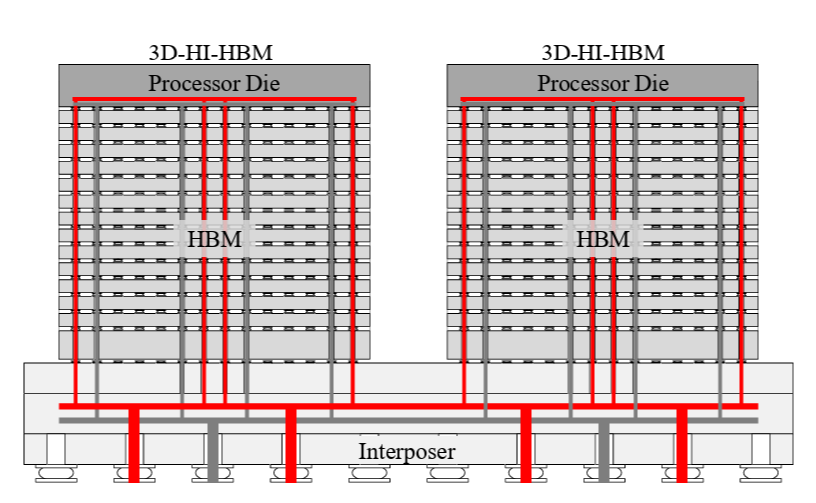
The schematic of the 3D-HI-HBM module featuring a multi-core processor stacked atop an HBM, integrated above a silicon interposer. Power is delivered to the topmost processor die through the 3D hierarchical PDN.
But the trade-off is obvious: how should power be delivered?
If the processor die sits on top of the HBM stack, the current required by high-performance logic cores must travel through the package substrate, interposer, TSVs, bumps, HBM regions, or bypass structures before reaching the top die. This is no longer a simple matter of drawing power planes on a substrate. It becomes a three-dimensional hierarchical PDN problem.
The paper builds a 3D hierarchical PDN model that considers the physical constraints of the package substrate, interposer, TSVs, decoupling capacitors, and power/ground bumps and planes. It uses unit-cell-based equivalent circuit modeling to analyze the system.
The key point is that the paper does not look at only one metric. It evaluates DC IR drop, frequency-domain impedance, and time-domain power switching noise at the same time.
This matters because a PDN that looks acceptable in DC analysis may still suffer from high-frequency switching noise. Conversely, if only high-frequency impedance is optimized, low-frequency behavior or stack-to-stack coupling may still become problematic.
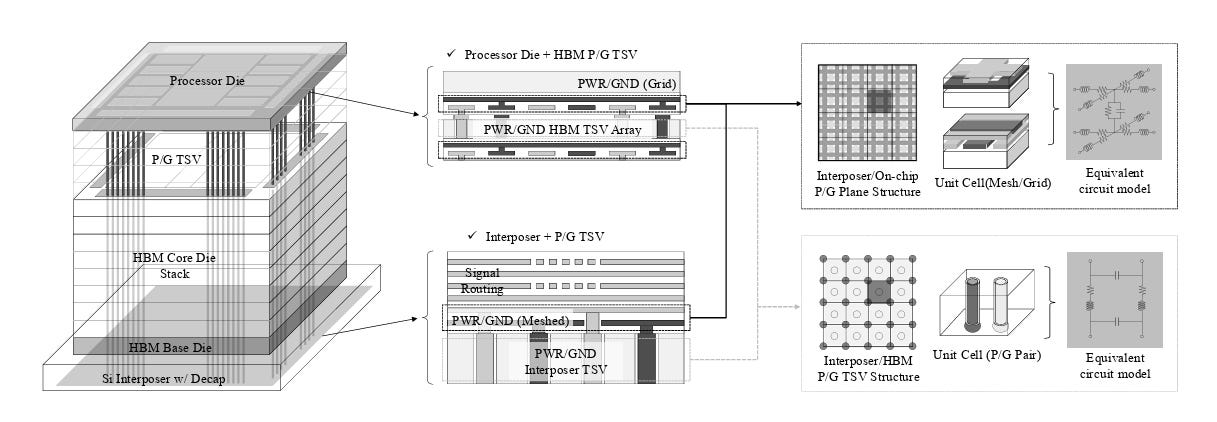
Design and modeling flow for the 3D hierarchical PDN of the 3D-HI-HBM module. Each component, including the P/G TSV array and P/G planes for the processor die, HBM base die, and interposer, is modeled as a repetitive array of unit cells. Each unit cell is represented by an equivalent RLC circuit model with frequency-dependent parameters.
One of the paper’s core findings is that physical-aware P/G TSV placement is critical. By placing P/G TSVs according to HBM core and bank regions, DC IR drop can be reduced from more than 10% of VDD to 3.7%. Peak voltage fluctuation can also be reduced from more than 10% to around 7%.
This shows that TSV placement is not simply a matter of adding more vertical connections. It must be designed together with HBM internal regions, logic load distribution, and current paths.
The second key finding concerns interposer-level PDN topology.
If a merged P/G plane is used at the interposer level, decoupling capacitance can be shared, which helps reduce self-induced noise. The paper notes that a merged PDN can reduce self-induced noise by 32%.
However, this creates another problem: stronger noise coupling between multiple 3D-HI-HBM stacks, resulting in an additional 11 mV transfer-noise penalty.
In other words, a shared power plane is like a shared reservoir. It improves efficiency, but load disturbances from one region can spread to another.
The paper therefore points to a more nuanced conclusion. The best power-integrity solution is not simply to merge or isolate everything. It requires co-optimization between high-density P/G TSV placement and interposer PDN isolation.
For multi-stack 3D-HI-HBM, low-frequency impedance, local IR drop, high-frequency switching noise, and stack-to-stack coupling must all be considered together.
The industry implication is important. This paper describes how HBM may evolve from 2.5D integration toward deeper 3D integration.

The IR drop voltage map at the top processor die for various P/G TSV placement designs are shown. By incorporating additional P/G TSVs at inter-channel and inter-bank areas, the worst-case voltage drop is improved from (a) 112.96 mV (14.12 %) to (b) 47.04 mV (5.88 %) and (c) 29.6 mV (3.70 %).
Today, mainstream AI GPUs usually place a large logic die and multiple HBM stacks side by side on an interposer or bridge-based package. In the future, if architectures move toward processor-over-memory, logic-near-memory, or more complex 3D stacked structures, PDN design will become one of the key barriers to commercialization.
Packaging teams will need to master not only high-speed routing, but also physical-aware design of three-dimensional power networks.

6月30日
HCB HBM: Interconnect Becomes Part of the Thermal Path

The third paper is Samsung’s“System-Level Thermal Characterization of Hybrid Cu Bonded HBM on 2.5D Advanced Packaging.”
This paper focuses on another highly practical constraint: thermal management.
When an AI or HPC package contains both a high-power ASIC or GPU and multiple HBM stacks, heat does not remain isolated on a single die. It couples across the HBM, ASIC, interposer, package, heat sink, and airflow environment.
Traditional HBM stacks often use TCB, or thermo-compression bonding, with micro-bumps. TCB is mature, but micro-bump pitch, resistance, parasitics, and thermal conduction paths all have limitations.
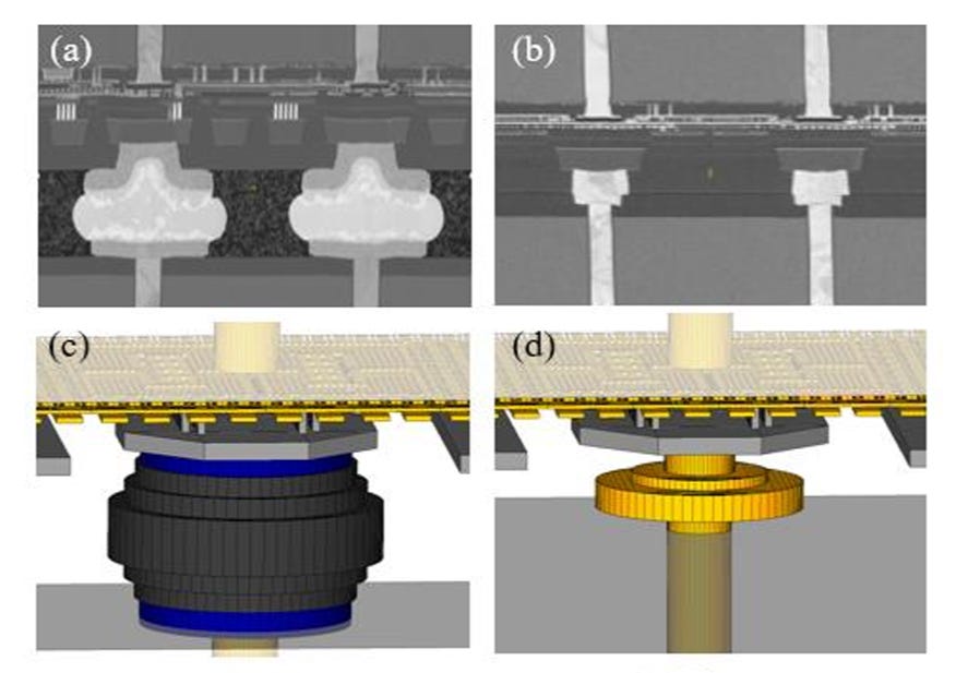
Actual structures of (a) TCB and (b) HCB, thermal models of (c) TCB and (d) HCB
HCB, or hybrid copper bonding, provides high-density interconnect through fine-pitch Cu-Cu and dielectric bonding. It is often discussed for its electrical benefits, such as lower interconnect resistance, higher I/O density, and shorter signal paths.

2025年1月20日
But this Samsung paper highlights another point: HCB can also be a thermal management technology.
The paper does not only measure a single junction thermal resistance. Instead, it builds a multi-scale numerical modeling methodology.
At the chip level, it analyzes detailed interconnect geometry, including metal connectivity and dielectric thin-layer effects. Then it transfers equivalent thermal properties into package-level and system-level simulations. Finally, it validates the model using HCB and TCB HBM test vehicles integrated with ASIC test vehicles on a silicon interposer under server-level air-cooling conditions.
This methodology is important because HBM thermal behavior cannot be judged from one scale alone.
At the chip level, joint density and materials determine vertical thermal resistance. At the package level, the relative position of HBM and ASIC, interposer heat spreading, TIM, and heat spreader design all influence heat flow. At the server level, airflow direction and uniformity create different thermal conditions across package locations.
If only a single test structure is evaluated, it may not reflect the real thermal interaction inside an AI server.
The paper shows that HCB has several advantages over TCB. It can reduce hotspot junction temperature, mitigate thermal crosstalk, and increase allowable power.
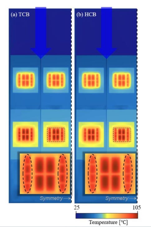
Temperature distribution at the package junction region under server-level conditions of 150 CFM airflow rate and 1032 W package power: (a) 2.5D package with TCB HBM and (b) 2.5D package with HCB HBM.
This means HCB does not only improve signaling. It also gives the system more power headroom.
For AI accelerators, allowable power is extremely important because system performance is often constrained by thermal design power. If the package interconnect itself can improve the thermal path, the entire module gains more performance margin.
The most concrete data comes from the pad-density parametric study. The paper shows that in the studied HCB joint pad configuration, doubling the joint pad count can reduce stack thermal resistance by 22.3% compared with a TCB HBM device. Increasing the joint pad count to four times can reduce stack thermal resistance by 29.1%.

Stack thermal resistance comparison between TCB and HCB HBM devices with varying joint pad density (P.D.) in HCB.
This result is important because it links I/O density with thermal conduction. More copper bonding pads do not only mean more electrical signal or power connections. They also create more vertical thermal paths.
This changes how we should think about interconnect.
In the past, package interconnect was often treated mainly as an electrical design problem: line width, spacing, impedance, loss, crosstalk, parasitic inductance, and capacitance. But in high-power 2.5D and 3D packages, interconnect is also part of the thermal, mechanical, and reliability structure.
When HCB pad density increases, both electrical and thermal performance may improve. But the design must also evaluate process yield, bonding defects, CTE mismatch, stress, and long-term reliability.
The paper also reminds us that HBM thermal design cannot be studied in isolation. When HBM and ASICs are placed together in the same SiP, ASIC heat affects HBM, and HBM heat affects the ASIC. If system airflow is uneven, downstream packages may experience higher thermal stress.
By providing better vertical heat spreading, HCB can reduce thermal coupling inside the SiP and improve the overall thermal environment for both HBM and ASICs.

2025年10月13日
HBM Is Entering the Era of Packaging Co-Design
Although these three papers focus on different topics — high-speed interconnect, power delivery, and thermal management — they point to the same conclusion: the next stage of HBM development depends on system-level co-design.
The first shared trend is that packaging is becoming the main battlefield for bandwidth scaling.
HBM4E requires data rates above 12 Gb/s and higher I/O counts. This is already beyond the comfort zone of conventional package routing. The emergence of technologies such as EMIB-T shows that high-bandwidth memory competition is no longer only about DRAM dies. It is also about bridges, TSVs, metal stacks, embedded decaps, and package architecture.
The second shared trend is that the boundary between 2.5D and 3D is becoming less clear.
In the past, 2.5D mainly meant placing logic and HBM side by side on an interposer. Now, research is beginning to explore logic stacked on HBM, or multiple 3D-HI-HBM modules integrated together. As vertical integration increases, data paths become shorter, but power delivery and thermal design become much harder.
The third shared trend is that SI, PI, and thermal design must be considered together.
EMIB-T’s MIM decap directly supports high-speed signal stability. 3D-HI-HBM’s P/G TSV placement affects both IR drop and switching noise. HCB pad density affects both I/O capability and thermal resistance.
These examples show that future advanced packaging can no longer follow a sequential model where electrical design is completed first and thermal design is treated as a later fix. From the earliest architecture stage, signal, power, thermal, mechanical, and process constraints must be placed on the same design map.
The fourth shared trend is that local optimization is no longer enough.
A single HBM stack with strong performance does not guarantee a good module. A single interconnect with low thermal resistance does not guarantee good server-level thermal behavior. A PDN with low impedance in one condition does not guarantee acceptable stack-to-stack coupling.
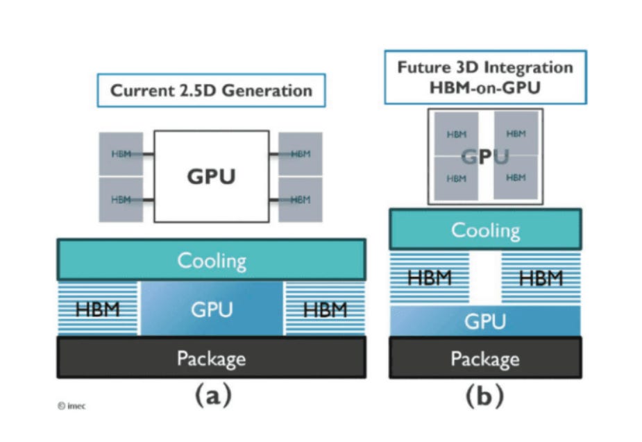
Imec has reported a major step forward in thermal management for future 3D HBM-on-GPU architectures. Using a system-technology co-optimization, or STCO, methodology, the research shows that cross-layer design can substantially lower GPU operating temperatures during AI training workloads. Presented at the 2025 IEEE International Electron Devices Meeting, the work indicates that optimized 3D integration, thermal-aware architecture design, and system-level co-design could reduce peak temperatures in advanced compute platforms from above 140°C to around 70°C.
AI and HPC packaging is becoming a multi-physics system engineering problem.
Implications for the Semiconductor Supply Chain
For chip design companies, HBM selection is no longer only about capacity and bandwidth specifications. The packaging platform must also be able to support the target bandwidth, power, thermal envelope, and yield.
If a design adopts an HBM4E-class interface, package routing, PDN, decap strategy, and thermal solutions must be included at the architecture definition stage.
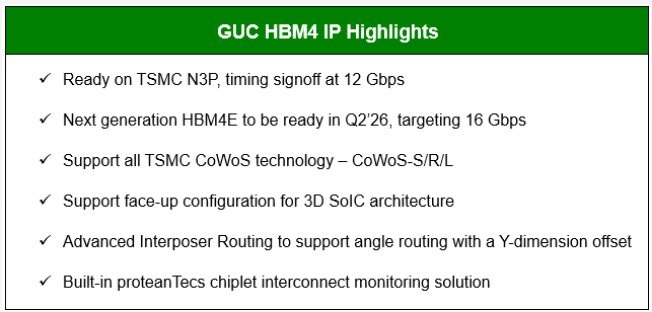
Global Unichip Corp. (GUC), the advanced ASIC leader, today announced the successful demonstration of a 12 Gbps HBM4 IP platform implemented on TSMC's 3nm process technology at the Partner Pavilion of the TSMC 2026 North America Technology Symposium. The platform features GUC's in-house full functional HBM4 Controller and PHY IP, integrated with a partner's HBM4 memory, and used TSMC's industry-leading CoWoS® advanced packaging technology.
For OSATs, foundries, and substrate suppliers, future competition will concentrate on high-density interconnect, low-loss materials, fine-line RDL, TSV and bridge processes, warpage control, thermal-path design, and reliability qualification.

Source: ASE

2025年6月18日
The ability to combine localized silicon bridges, organic substrates, glass substrates, silicon interposers, and HCB effectively will become a major source of product differentiation.
For memory suppliers, the HBM stack itself remains critical, but co-optimization with logic will become increasingly important. HBM is no longer an independent component. It is part of the full AI accelerator package.
Future HBM suppliers will need deeper co-development with foundries, OSATs, substrate vendors, and system companies.

Source: TSMC
For system vendors and data center operators, package-level power and thermal design will directly affect rack-level performance.
If the package can tolerate higher power, reduce thermal coupling, and improve airflow efficiency, the system can deliver higher performance per watt under the same cooling constraints.
HBM Shortages Are Pushing Vendors Toward LPDDR Alternatives
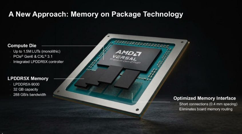
The ongoing shortage of HBM is forcing more semiconductor vendors to rethink how they design high-performance memory architectures. While HBM remains the preferred solution for maximum bandwidth, its limited supply, high cost, and dependence on advanced packaging capacity have made it difficult to use across every product category. As a result, some companies are turning to LPDDR as a more available and supply-chain-friendly alternative.
AMD’s Versal Premium Gen 2 Memory on Package is a clear example of this shift. Instead of using HBM, AMD’s latest generation of memory-on-package programmable logic devices adopts LPDDR5X. From a hardware perspective, this is a trade-off: AMD gives up memory bandwidth in exchange for better availability, simpler packaging, and longer-term supply stability.
The production advantages are meaningful. LPDDR5X is used across a much wider range of products than HBM, which means the three major memory suppliers are likely to keep it in production for a longer period. Over time, supply may also expand to second-tier memory vendors such as Nanya, Winbond, and Chinese suppliers like CXMT.
LPDDR5X also reduces packaging complexity. HBM-based designs typically require advanced packaging technologies such as CoWoS and silicon interposers. By placing LPDDR5X on package, AMD can use more conventional organic packaging, helping its adaptive SoC products avoid another major bottleneck: limited advanced packaging capacity.
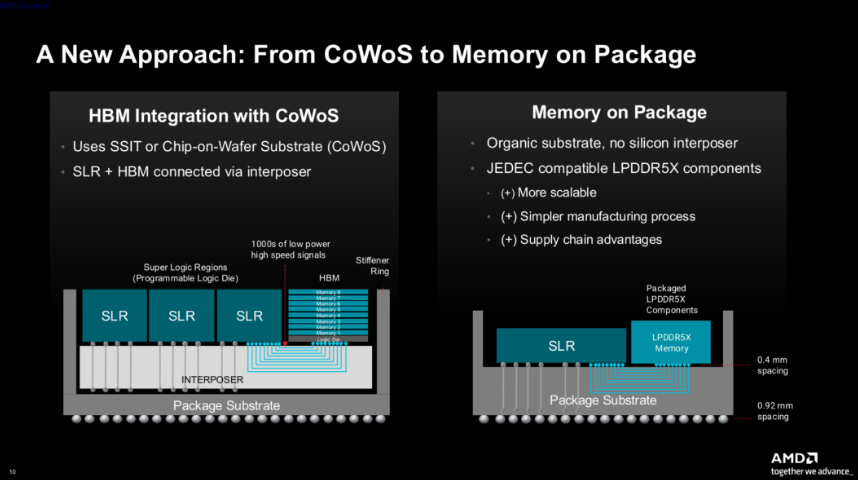
There is also a design efficiency benefit. AMD’s high-end Versal Premium Gen 2 silicon already includes a 256-bit DDR5/LPDDR5X memory controller, meaning the company does not need to create a separate die just for this product variant. That simplifies production planning and reduces the need to maintain multiple die versions over a long product lifecycle.
The compromise is memory bandwidth. AMD’s previous Versal HBM products offered up to 32GB of memory with 819GB/s of bandwidth. The new Versal Gen 2 Memory on Package devices still offer 32GB of memory, but bandwidth drops to 288GB/s with LPDDR5X. In other words, memory capacity remains comparable, but bandwidth is significantly lower.
This reflects a broader industry reality: in the AI and high-performance computing era, HBM is becoming a scarce strategic resource. Not every product can justify using it, especially when HBM supply is prioritized for GPUs, AI accelerators, and data center systems. For many applications, LPDDR may become the practical compromise—less bandwidth, but better availability, lower packaging complexity, and a more stable supply chain.

2月14日
Conclusion: The Future of HBM Is a Packaging Architecture Race
HBM technology is shifting from “faster memory” to “more complete system packaging.”
Intel’s EMIB-T paper shows that 12+ Gb/s HBM4E requires the combined support of bridge architecture, TSV-based power delivery, and embedded decoupling. KAIST’s 3D-HI-HBM paper shows that once processors and HBM are vertically integrated, the power network must become a three-dimensional, physical-aware design problem. Samsung’s HCB HBM paper shows that hybrid copper bonding can improve not only electrical performance, but also thermal paths for high-power packaging.
The key to future HBM will not be a single breakthrough. It will be whether the entire packaging platform can solve three problems at the same time: whether high-speed signals can remain stable, whether clean power can be delivered to the right location, and whether heat can be removed efficiently.
The companies that can integrate these three capabilities into a manufacturable, scalable, and cost-effective architecture will be better positioned to win the next stage of AI and HPC semiconductor competition
Thanks for reading SEMIVISION @_@! This post is public so feel free to share it.


Previous