Who Controls HBM Controls the AI Semiconductor Era
Who Controls HBM Controls the AI Semiconductor Era
- Source: SemiVision
- Author: SEMIVISION
- Published: 2026-06-30T10:56:54+08:00
- URL: https://tspasemiconductor.substack.com/p/who-controls-hbm-controls-the-ai (1) Who Controls HBM Controls the AI Semiconductor Era


Who Controls HBM Controls the AI Semiconductor Era
Original Article By SemiVision Research [Reading time: 9 mins]

Jun 30, 2026
Who Controls HBM Controls the AI Semiconductor Era

Memory is no longer a supporting component. It is becoming the gatekeeper of AI infrastructure.
The semiconductor market in 2026 is no longer well described by the old hierarchy in which CPUs and GPUs were the protagonists and memory was merely a supporting component. In the current AI infrastructure cycle, the real shift in industry power is coming from something more structural: high-bandwidth memory and advanced packaging are increasingly determining whether an AI system can ship on time, whether a platform can pass validation, and whether hyperscalers can keep scaling capex without losing efficiency.
Several developments over the last few weeks make that shift unusually clear. Samsung said on May 29, 2026 that it had begun shipping 12-layer HBM4E samples to major customers.
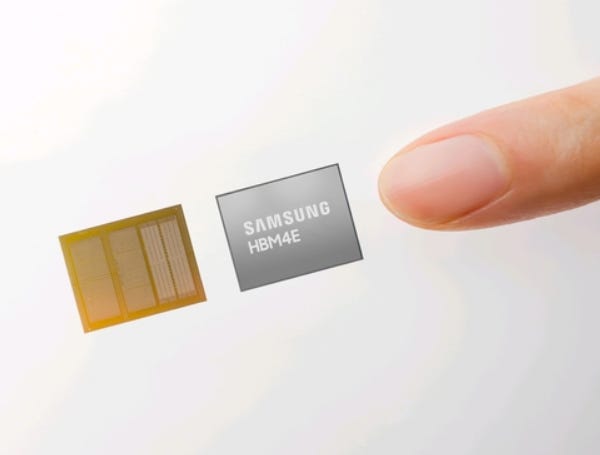
SK hynix followed on June 18 with its own announcement that 12-layer HBM4E samples had been delivered to major customers. On June 24, Micron added the financial layer to the story by reporting record fiscal Q3 2026 results and emphasizing the strategic value of memory in the AI era, while also highlighting multi-year Strategic Customer Agreements intended to improve the predictability of future performance.

Taken together, these developments signal that HBM is no longer just a component that ships alongside AI accelerators. It is becoming a strategic asset that customers must reserve early, suppliers can contract earlier, and capital markets are increasingly willing to value as infrastructure rather than commodity output.

6月11日
The competitive question is shifting from capability to reliable delivery
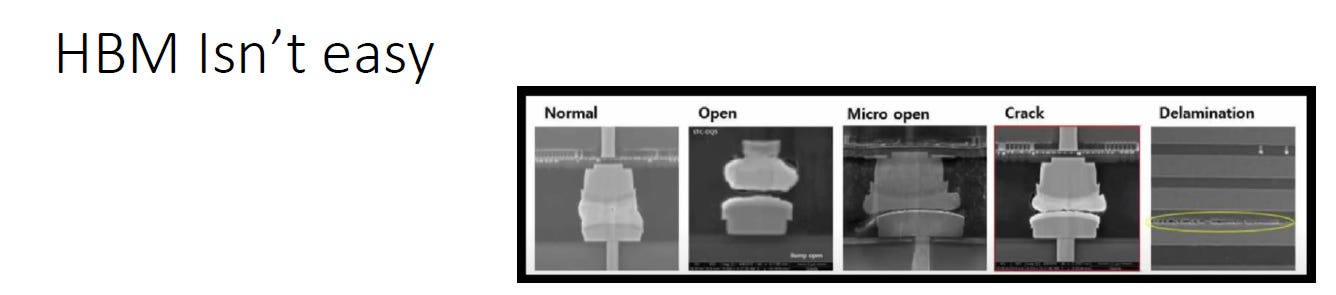
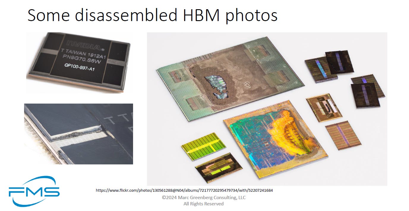
HBM is not just DRAM stacking.It is a full 3D integration process that combines DRAM dies, TSVs, micro-bumps, bonding, interposers, and advanced packaging.
Ultra-thin die handling is extremely difficult.Each DRAM die must be thinned before stacking, making it fragile and vulnerable to cracking, chipping, warpage, and handling damage.
TSV formation requires very high precision.Through-silicon vias must be etched, insulated, filled, and connected correctly. Any void, misalignment, or contamination can cause electrical failure.
Micro-bump bonding is a major yield risk.HBM stacks contain thousands of tiny vertical interconnects. Defects such as open joints, micro-opens, cracks, and delamination can kill the stack.
Stack alignment must be extremely accurate.Multiple DRAM dies must be aligned at micron-level precision. A small overlay error can damage signal paths or reduce yield.
Thermal stress is difficult to control.Different materials expand and contract at different rates during bonding, reflow, and operation. This can create cracks, warpage, or interface separation.
Heat dissipation becomes harder as stack height increases.Inner DRAM layers are farther from the heat sink, making thermal management more difficult than in conventional planar DRAM.
Power delivery is challenging.Stable power must be delivered vertically through the stack. IR drop, current crowding, and local hot spots can affect reliability and performance.
Signal integrity must be tightly controlled.HBM uses massive parallel data paths. Crosstalk, impedance mismatch, timing skew, and noise can all degrade performance.
Yield loss compounds across layers.If one die or one bonding layer fails, the entire HBM stack may become unusable. Higher stack counts increase cumulative yield risk.
Testing is complex and expensive.HBM must be tested at wafer level, stack level, package level, and system level. Some defects are difficult to detect until after integration.
Packaging dependency is high.HBM performance depends not only on the memory itself, but also on interposers, substrates, CoWoS-like packaging, and integration with GPUs or AI accelerators.
The manufacturing barrier is structural.HBM requires deep know-how in DRAM process technology, materials, equipment, metrology, bonding, packaging, and high-volume yield control.
This is why only a few companies can supply HBM at scale. The challenge is not just designing memory. It is producing reliable, high-bandwidth, high-capacity 3D memory stacks at commercial yield.
That is why the recent announcements from Samsung and SK hynix did not focus only on peak speed or capacity. They also emphasized power efficiency, thermal characteristics, process maturity, and alignment with customer schedules. AI data center operators are not buying theoretical bandwidth. They are buying deployable infrastructure that must run dense workloads for long periods without creating unacceptable power or thermal penalties.
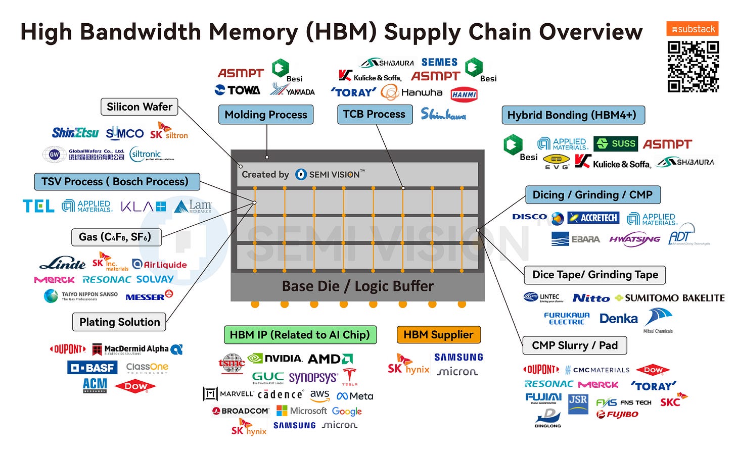
This changes the distribution of value across the supply chain. The winning formula now spans DRAM process technology, advanced-node logic base dies, packaging integration, test capacity, thermal engineering, and substrate availability. HBM competition is therefore rewriting not only product roadmaps, but also profit pools across the memory ecosystem.

6月28日
Long-term contracts are pulling memory away from the old commodity cycle
Micron’s latest messaging is especially important because it gives the market a language for what many participants already suspected: supply for advanced AI memory is moving away from purely short-cycle pricing logic and toward multi-year strategic allocation.
That shift has a simple economic cause. When HBM becomes a gating factor for AI server deployment, customers worry less about paying somewhat higher prices and more about not securing enough supply, missing validation windows, or delaying rack deployment. Once that happens, long-term supply agreements become a rational response rather than a special case.
This has at least three consequences.
First, revenue visibility for memory suppliers improves, which supports larger capital expenditure programs and makes those programs easier for investors to underwrite.
Second, GPU vendors and hyperscalers move upstream in the planning process. They no longer behave like buyers of interchangeable components; they become co-architects of supply timing.
Third, pricing starts to reflect strategic allocation and platform importance, not just conventional memory-cycle volatility.
This is also why equity markets have rewarded companies more directly exposed to HBM leadership. The June 22 report that SK hynix overtook Samsung Electronics by common-share market capitalization was not just a stock-market curiosity. It was a visible sign that investors are re-rating the companies most closely tied to AI memory bottlenecks and execution.

Reuters: Shares of SK Hynix, now the world's most valuable memory chipmaker, closed up 5.6%, lifting its market capitalisation to 2,080.4 trillion won ($1.35 trillion), while Samsung's stock eased 0.14% to give it a market value of 2,066.7 trillion won, excluding preferred shares.
The HBM boom is spilling into the rest of the memory market
The upside of AI memory also comes with system-wide tradeoffs. When fabs, engineering talent, equipment budgets, packaging resources, and management attention are increasingly directed toward HBM, other memory categories can feel the strain. Mature DRAM, selected specialty memory segments, and non-AI end markets may face supply tightness or rising costs even if they are not direct HBM consumers.
This is one of the most important second-order effects to watch through 2026 and 2027. AI does not only raise the bill of materials for AI servers. It can re-price memory across adjacent sectors by reallocating wafer starts, packaging capacity, and development priorities.
For the broader supply chain, especially in Taiwan and the rest of Asia, this matters a great deal. Advanced packaging houses, substrate vendors, thermal solution providers, test and burn-in players, and related equipment suppliers sit directly in the path of this value migration. As customers move to reserve supply earlier and for longer durations, bargaining power may rise in parts of the downstream ecosystem that were previously seen as operational support rather than strategic chokepoints.
More spending does not automatically mean fast relief
SEMI’s latest data show how aggressively the industry is trying to catch up. Global semiconductor equipment billings in Q1 2026 rose 14% year over year to $36.55 billion. SEMI also projected global 300mm fab equipment spending to rise 18% in 2026 to $133 billion and another 14% in 2027 to $151 billion.
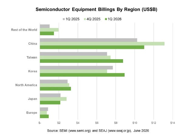
Those are large numbers, but they should not be misread as proof that supply will soon become abundant. In AI memory, capacity expansion is not linear. Spending must translate into buildings, tool installs, yield ramp, customer qualification, packaging readiness, and thermal reliability. HBM is not only a front-end wafer problem. It is equally a back-end integration and system-validation problem.
That means the most likely scenario for the next several quarters is not oversupply. It is continued expansion alongside continued structural tightness. This is exactly why the market is seeing sample activity, long-term contracts, and co-development arrangements at the same time.
The bottleneck is time-to-usable-capacity, not merely headline wafer investment.
Policy is becoming part of supply strategy
There is also a policy layer worth watching very closely. In its January 14, 2026 proclamation on semiconductor imports, the White House directed the Secretary of Commerce to provide, by July 1, 2026, an update on the market for semiconductors used in U.S. data centers so the President could determine whether the existing tariff approach should be modified. As of June 29, 2026, that update had not yet been formally released.
Why does that matter for memory? Because data center chip policy does not affect only accelerators. It can influence customer planning horizons, regional sourcing decisions, supply-chain localization, and the urgency with which large buyers secure future capacity. Policy uncertainty often reinforces pre-booking behavior, and pre-booking behavior strengthens the strategic position of suppliers with the most credible execution.

dcmap.u
U.S. data centers are entering a constraint-driven growth phase. AI demand remains strong, but the bottleneck has shifted from land and servers to power, permitting, grid interconnection, and cooling. Data center electricity demand is projected to push U.S. power consumption to record highs in 2026 and 2027, while regulators are considering faster connection rules for very large loads. At the same time, vacancy in key markets such as Northern Virginia is extremely tight, showing that demand still exceeds available capacity. The strategic winners will be operators that can secure power, chips, cooling, and local political support early.

4月16日
The new winners will be the companies that can orchestrate the stack
The next phase of the semiconductor race will not be won only by the company that designs the highest peak compute. It will be won by the companies that can orchestrate compute, memory, packaging, thermals, contracts, and geopolitics into a deliverable AI infrastructure stack.
From that perspective, HBM4E sample shipments are only the visible tip of the story. The deeper shift is that memory is moving from a cost line item to a gatekeeper asset. Over the next one to two years, the GPU vendors, hyperscalers, and system companies that secure stable access to HBM and advanced packaging may enjoy a stronger competitive position than those focused only on peak silicon performance.
For memory suppliers, technology leadership still matters. But the real conversion metric is whether technology leadership can be turned into strategic contracts, production cadence, and supply-chain control. If that conversion continues, the result will not just be higher HBM pricing. It will be a broader repricing of the semiconductor value chain, with new valuation frameworks, new capex priorities, and a different allocation of profits across the industry.
That is why the most important semiconductor story today is not simply a new memory product launch. It is the emergence of HBM as a strategic asset class in the AI era.

Source: SK Hynix
Key indicators to watch next
Updated HBM4 and HBM4E production timelines from Micron, SK hynix, and Samsung in the second half of 2026.
Additional long-term supply, co-development, or capacity reservation disclosures involving NVIDIA, AMD, and major cloud service providers.
New signs of constraint or expansion across CoWoS, advanced packaging, ABF substrates, and thermal management.
Whether the U.S. issues a concrete data-center semiconductor policy update on or around July 1, 2026.
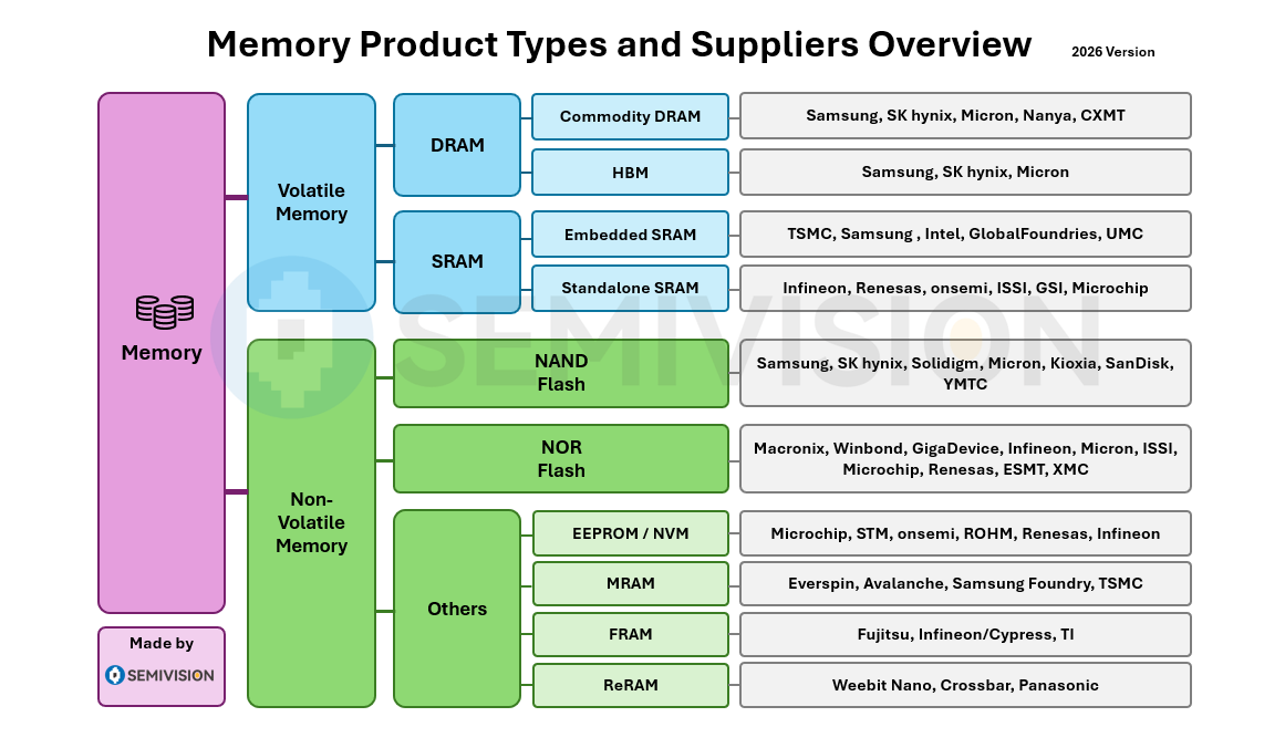
Whether AI-driven resource allocation continues to tighten pricing in DDR4, LPDDR, and specialty memory categories.

6月18日


PreviousNext