AI Chips Are Hard. Memory Is Harder.
AI Chips Are Hard. Memory Is Harder.
- Source: SemiVision
- Author: SEMIVISION
- Published: 2026-06-28T13:47:40+08:00
- URL: https://tspasemiconductor.substack.com/p/ai-chips-are-hard-memory-is-harder (1) AI Chips Are Hard. Memory Is Harder. - SEMIVISION @_@


AI Chips Are Hard. Memory Is Harder.
Original Article By SemiVision Research [Reading time: 7 mins]

Jun 28, 2026
AI Chips Are Hard. Memory Is Harder.
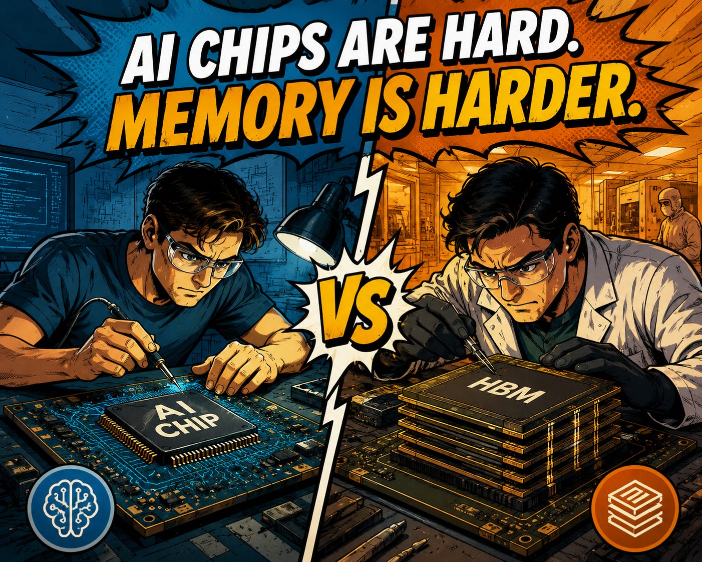
The biggest misconception in today’s semiconductor industry is that designing AI chips is the pinnacle of engineering difficulty.
It is not.
In reality, the technology that has proven far more difficult to master—and far more resistant to new entrants—is memory.

The rapid emergence of custom AI chips from cloud service providers has reinforced this misconception. Companies such as Google, Meta, Microsoft, Amazon, Tesla, Open AI and countless startups are now developing their own AI accelerators. This has created the impression that semiconductor design has become democratized.
Yet if we look at the memory industry, the story is completely different.
After decades of consolidation, the world’s advanced DRAM market is still dominated by only three companies. The number of suppliers capable of mass-producing high-bandwidth memory (HBM), the most strategic component of AI infrastructure, remains exactly the same.
The contrast is striking.
If AI chips are truly the hardest products in semiconductors, why are dozens of companies able to build them while almost nobody can build memory?
The answer reveals one of the deepest truths about semiconductor manufacturing.

3月25日
Logic Chips Can Be Outsourced. Memory Cannot.
When people say a company is “developing its own chip,” they usually mean a logic chip—a CPU, GPU, AI accelerator, networking ASIC, or custom processor.

Source: hackernoon
These chips certainly require extraordinary engineering expertise.
None of this is easy.
However, one enormous advantage exists.
Most companies do not need to manufacture these chips themselves.
Instead, they rely on foundries such as TSMC to transform digital designs into physical silicon.
This separation between design and manufacturing fundamentally lowers the barrier to entry.
A startup with a brilliant architecture can leverage the same advanced manufacturing technology used by the world’s largest semiconductor companies.
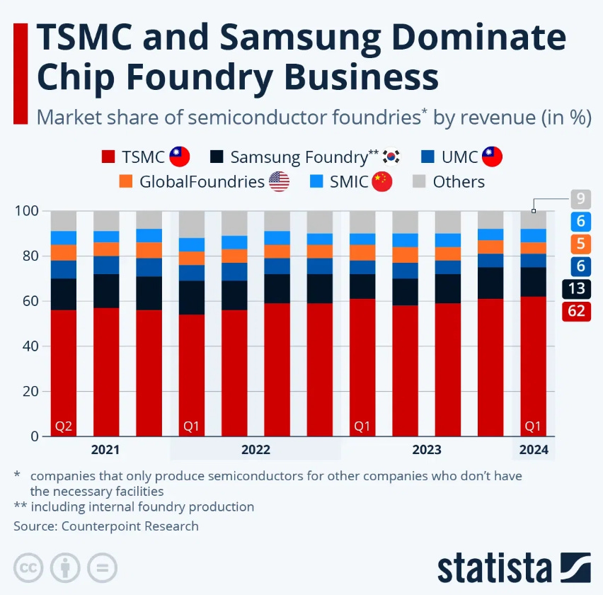
The foundry ecosystem, combined with mature EDA software and licensable IP from companies such as Arm, has dramatically accelerated innovation.
Memory does not work this way.
Memory Is Not Just a Chip. It Is a Manufacturing System.
Unlike logic semiconductors, advanced DRAM production is almost entirely based on the integrated device manufacturer (IDM) model.

The companies designing the memory are also responsible for inventing the process technology, developing manufacturing recipes, optimizing equipment parameters, and continuously improving yield.
There is no equivalent of a “TSMC for DRAM.”
A company cannot simply finish a DRAM design and send it to an external manufacturer.
Instead, it must master every layer of production itself.
That includes capacitor formation, cell architecture, leakage control, lithography integration, process chemistry, defect management, refresh optimization, reliability engineering, and manufacturing yield.
Many of these technologies are accumulated through decades of production experience rather than written documentation.
Some of the industry’s most valuable knowledge exists only as tacit know-how inside manufacturing teams.
Money alone cannot buy it.

2025年10月13日
Yield Is the Ultimate Barrier
The greatest challenge in memory manufacturing is not designing a working cell.
It is producing billions of identical cells with almost perfect consistency.
A modern AI processor may contain over one hundred billion transistors.
A DRAM chip contains an even larger number of memory cells that are nearly identical.
Every one of those cells must behave correctly.
Even microscopic process variation can introduce leakage, retention problems, or bit failures.

Source: AMAT
Unlike logic chips, where redundancy is relatively limited, memory products are extraordinarily sensitive to manufacturing defects because every defective cell directly reduces usable capacity or long-term reliability.
As process nodes continue shrinking, maintaining acceptable defect density becomes exponentially more difficult.
Success depends not only on transistor scaling but on manufacturing discipline across thousands of process steps.
This is why DRAM manufacturing is often described as a yield business rather than simply a design business.
HBM Raises the Difficulty Again
If conventional DRAM is already difficult, High Bandwidth Memory represents another level entirely.
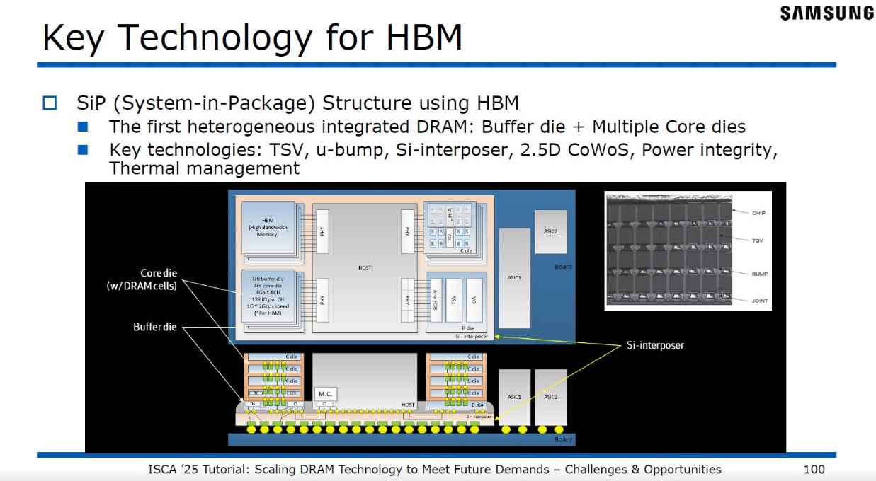
HBM combines advanced DRAM fabrication with sophisticated three-dimensional packaging technologies.
Modern HBM requires through-silicon vias (TSVs), wafer thinning, precision stacking, thermal optimization, advanced signal integrity, and increasingly sophisticated bonding technologies.
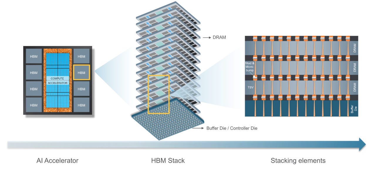
Source: AMAT
Every additional memory layer increases manufacturing complexity.
Every interface introduces another opportunity for yield loss.
The challenge is no longer limited to producing excellent DRAM dies.
Manufacturers must also integrate multiple dies into a single package while maintaining electrical performance, mechanical reliability, and thermal efficiency.
The result is one of the most complicated semiconductor products ever commercialized.
This explains why only three companies currently supply HBM at meaningful scale despite enormous global demand.

2月13日
Why So Many Companies Can Build AI Chips
Ironically, AI has made custom chip development easier from a business perspective.
Hyperscalers no longer need to compete directly with Nvidia by building general-purpose GPUs.
Instead, they can optimize chips for their own workloads.
Google develops Tensor Processing Units.
Amazon builds Trainium and Inferentia.
Microsoft is investing in Maia.
Meta is designing its own AI accelerators.
Tesla continues expanding its Dojo architecture.
Open AI builds Jalapeño with Broadcom.

OpenAI unveils first chip as part of Broadcom deal in effort to ‘build the full stack
Each company focuses primarily on architecture, software optimization, memory hierarchy, networking integration, and workload efficiency.
Manufacturing remains the responsibility of world-class foundries.
This division of labor dramatically reduces the complexity required for successful product development.
The innovation barrier shifts from process engineering toward system architecture.

4月7日
NAND Flash Sits Between the Two Worlds
Flash memory occupies an interesting middle ground.
Three-dimensional NAND manufacturing is extraordinarily complex, requiring hundreds of stacked layers and highly specialized process integration.
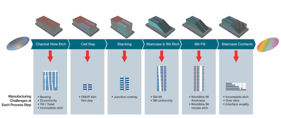
3D NAND structure manufacturing challenges at each step / Thermofisher
However, compared with advanced DRAM—and especially HBM—it generally presents slightly lower barriers in manufacturing consistency and packaging integration.
One reasonable way to view semiconductor difficulty today is:
HBM → DRAM → NAND Flash → Custom Logic ASIC
Each step upward requires not only stronger engineering capabilities but also deeper manufacturing expertise accumulated over decades.

The Future Semiconductor Race Is No Longer Just About Chips
The AI era is changing how the semiconductor industry measures competitive advantage.
During previous decades, the spotlight belonged to processors.
Today, memory increasingly determines the practical limits of AI infrastructure.
A GPU without sufficient HBM cannot deliver its theoretical performance.
An AI data center without enough memory cannot fully utilize its compute capacity.
As model sizes continue growing, memory bandwidth and capacity are becoming as strategically important as compute itself.
This explains why memory suppliers have become some of the most valuable companies in the semiconductor industry.

5月18日
SemiVision View
But history suggests that the true moat lies elsewhere.
Logic chips can increasingly leverage standardized design ecosystems, commercial IP, and world-class foundries.
Memory cannot.
Memory is where manufacturing expertise, materials science, process integration, yield engineering, and decades of accumulated know-how converge into an almost insurmountable barrier.
This is why new AI chip companies continue to emerge every year, while the list of companies capable of manufacturing leading-edge DRAM or HBM has barely changed for decades.
The next chapter of semiconductor competition will not simply be defined by who builds the fastest processor.
It will be defined by who controls the hardest manufacturing capability in the AI era. And increasingly, that capability is memory.
More and more companies are developing their own AI chips.
The number of companies capable of producing DRAM, however, has barely increased.
When it comes to High Bandwidth Memory (HBM), the industry is still dominated by just three suppliers (SK Hynix, Samsung, Micron).
This reflects a fundamental reality of the semiconductor industry. The capability to design logic chips can be built progressively by leveraging mature EDA tools, licensable IP, and the foundry ecosystem. Advanced memory, however—particularly DRAM and HBM—requires decades of accumulated expertise in process integration, materials engineering, manufacturing equipment, yield optimization, and high-volume production. These capabilities cannot simply be purchased or outsourced.
As a result, if we compare the technological barriers to achieving true end-to-end independence, the ranking is clear:
Self-developed HBM > Self-developed DRAM > Self-developed NAND > Self-developed AI ASIC / CPU
This also explains why the number of companies capable of supplying advanced AI memory remains far smaller than the number of companies capable of designing AI processors. In the AI era, the ultimate competitive moat is no longer just chip architecture—it is manufacturing know-how.

5月12日

4月15日


PreviousNext