From Toilets to Chips: How TOTO Became a Hidden Semiconductor Materials Champion
From Toilets to Chips: How TOTO Became a Hidden Semiconductor Materials Champion
- Source: SemiVision
- Author: SEMIVISION
- Published: 2026-06-23T10:11:45+08:00
- URL: https://tspasemiconductor.substack.com/p/from-toilets-to-chips-how-toto-became (1) From Toilets to Chips: How TOTO Became a Hidden Semiconductor Materials Champion


From Toilets to Chips: How TOTO Became a Hidden Semiconductor Materials Champion
Original Article By SemiVision Research [Reading time: 14 mins]

Jun 23, 2026
∙ Paid
From Toilets to Chips: How TOTO Became a Hidden Semiconductor Materials Champion

Most people know TOTO because of toilets.
In luxury hotels, TOTO’s smart toilets—capable of automatic lid opening, seat heating, washing, and deodorizing—have almost become a symbol of Japanese manufacturing. But the most interesting thing about the AI era is this: the companies that make the real money are not necessarily the visible consumer brands, nor even the GPU companies standing on stage. Often, they are the materials companies hidden deep inside the manufacturing process, companies that may appear to have nothing to do with semiconductors at first glance.

TOTO Washlet G5A Integrated Smart Toilet
TOTO is one of the best examples.
On the surface, TOTO is a bathroom fixtures brand. But at its core, it is also a materials company that understands ceramics, sintering, surface control, and mass-production stability. According to TOTO’s official materials, its Advanced Ceramics Division was established in 1984 and has long supplied industrial ceramic products for applications including semiconductors and optical communications. Its main products include electrostatic chucks, ceramic AD films, engineering ceramics, and bonding capillaries.
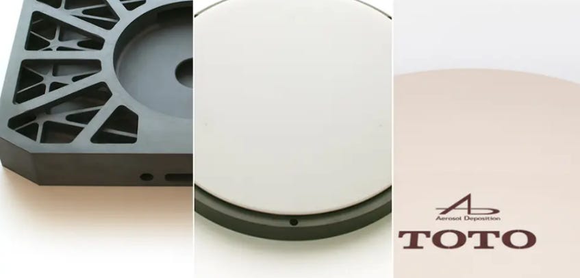
This is the core of TOTO’s transformation: it did not suddenly jump into semiconductors. Instead, it gradually transferred its ceramic capabilities from “making toilets” to “making critical components for wafer manufacturing equipment.”
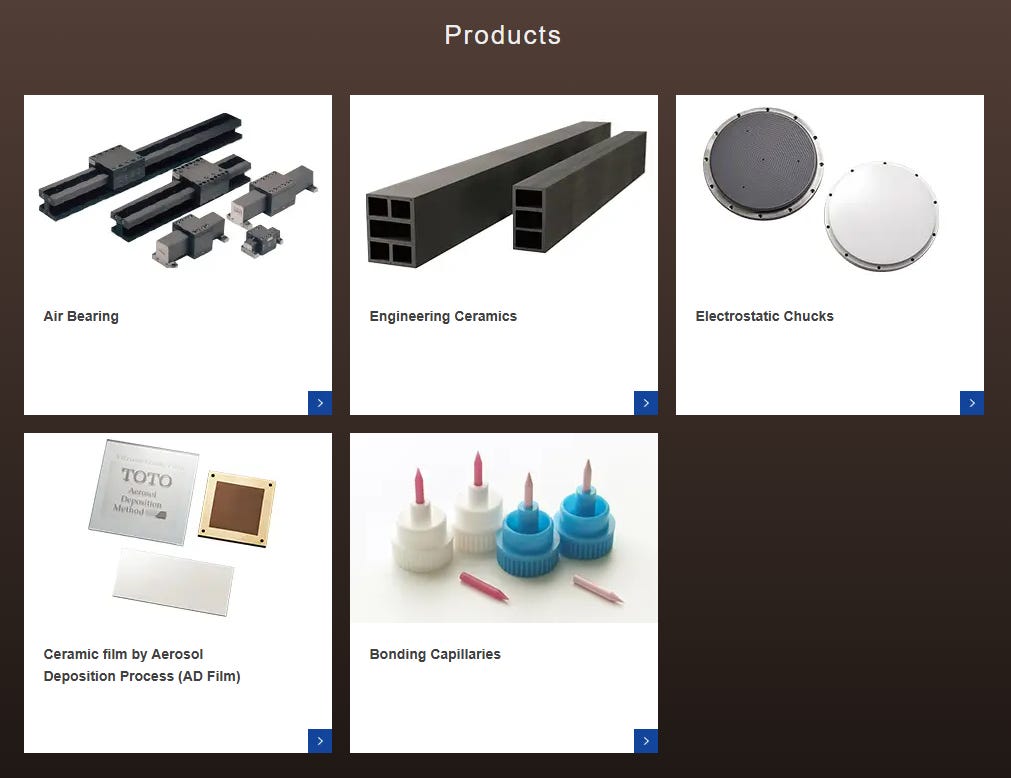

Below we will share:
Toilets and Semiconductors Are Actually Testing the Same Thing: Materials Control
What Is an Electrostatic Chuck?
Why Are Materials So Important?
ESCs Have Two Main Technical Routes: Coulomb and Johnsen-Rahbek
Semiconductor Ceramics Have Become TOTO’s High-Margin Growth Engine
Why Is AI Driving TOTO? The Answer Lies in Memory and Etching


6月22日
Toilets and Semiconductors Are Actually Testing the Same Thing: Materials Control
When many people hear that TOTO is involved in semiconductors, their first reaction is disbelief: how can a toilet company enter the wafer fab?
But from a materials perspective, this is not strange at all.
What problems must sanitary ceramics solve? High-temperature sintering, surface flatness, corrosion resistance, stain resistance, and long-term durability without degradation. What problems must ceramics for semiconductor equipment solve? High purity, plasma resistance, heat resistance, low contamination, dimensional stability, and long-term reliability.
The application scenarios are different, but the underlying capabilities are very similar.
Semiconductors are not only about chip design, EUV, CoWoS, or HBM. What truly supports advanced manufacturing is an entire ecosystem of materials and equipment. During etching, deposition, cleaning, metrology, and wafer handling, every wafer must remain stable. It cannot shift, become contaminated, or suffer from uneven heating. The more advanced the process node becomes, the less it is simply about “placing a wafer on a tool and processing it.” Instead, it becomes a matter of controlling wafer position, temperature, surface particles, and process stability with extremely high precision.
One of TOTO’s core products in this field is theelectrostatic chuck.

What Is an Electrostatic Chuck? It Is Not a Supporting Component — It Is the Foundation of Wafer Processing
If semiconductor manufacturing is like a high-precision surgical operation, then the wafer is the patient, etching, deposition, and ion implantation are the surgical instruments, and the electrostatic chuck is the operating table.
But this operating table cannot simply hold the wafer in place. It must firmly secure the wafer under vacuum, high temperature, low temperature, plasma, corrosive gases, and high electric fields. At the same time, it must control wafer temperature, reduce backside particle contamination, maintain wafer flatness, and ensure that the process can be repeated stably across thousands or even tens of thousands of wafers.
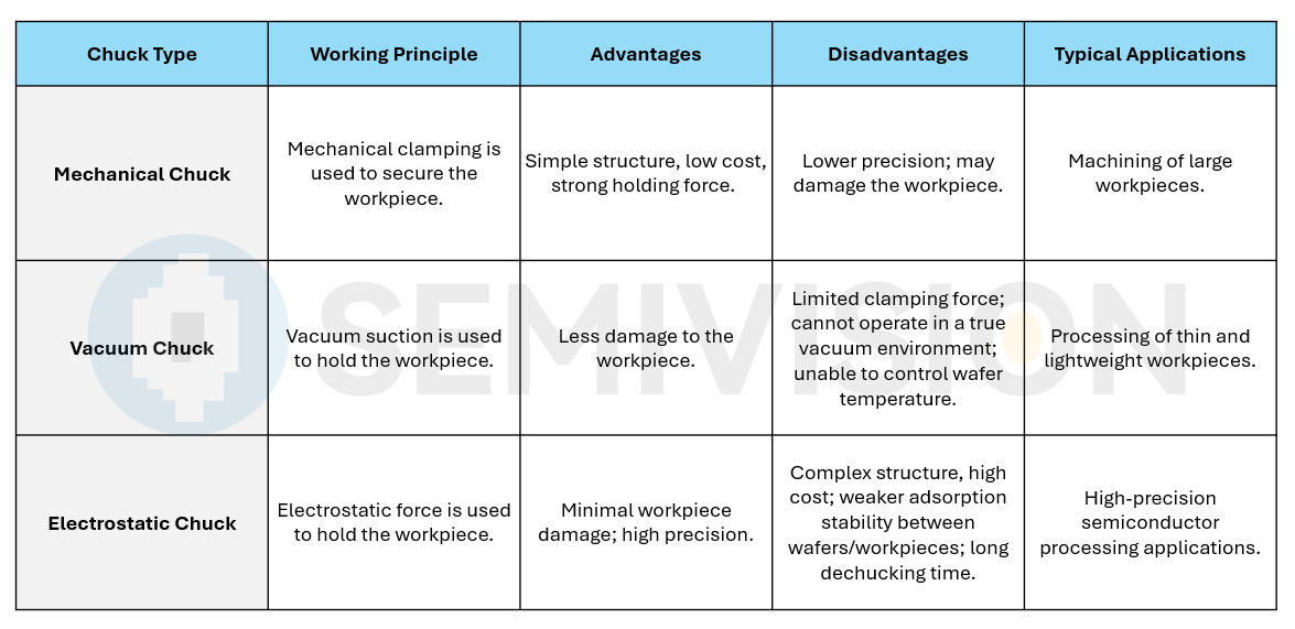
This is the electrostatic chuck, commonly abbreviated as ESC.
The basic principle of an ESC is to apply voltage between the wafer and the internal electrode inside the chuck. Through a dielectric layer, this forms a structure similar to a parallel-plate capacitor, generating electrostatic attraction that clamps the wafer onto the ceramic surface. This structure is commonly used in dry etching, vacuum CVD, and ion implantation equipment. It is not merely an auxiliary component for wafer handling; it is a core component that determines process stability.
The real challenge of ESC technology is not “holding” the wafer — it is holding it stably.
Wafer processing is most vulnerable to two problems: wafer position instability and wafer temperature instability.
In plasma etching, the wafer surface is affected by ion bombardment and chemical reactions. If the wafer is not uniformly clamped, some local areas may have poor contact with the chuck surface, leading to non-uniform temperature distribution. Once temperature becomes uneven, etch rate, critical dimension control, selectivity, and uniformity may all be affected. For advanced logic, DRAM, and 3D NAND, this is not a minor issue. It is a process variable that directly affects yield.
That is why an ESC is not just a ceramic plate that can hold a wafer. It is also a thermal management platform.
In actual equipment, ESCs are usually used together with backside gas cooling. This means that an inert gas with high thermal conductivity, commonly helium, is introduced to the backside of the wafer, forming a controllable thermal transfer path between the wafer and the chuck. Research has shown that the cooling efficiency of the ESC/BSG system depends on the thermal transfer capability of the backside gas and the uniformity of wafer clamping on the chuck. The greater the wafer warpage, the higher the risk of backside gas leakage and clamping failure, which in turn increases the possibility of wafer overheating.
This is where the technological barrier of ESC becomes clear: it simultaneously involves electric fields, materials, heat transfer, mechanical flatness, and process chemistry.
Why Are Materials So Important?
The main body material of an electrostatic chuck is usually a high-performance ceramic, such as aluminum oxide or aluminum nitride. These materials must offer high mechanical strength, good thermal conductivity, thermal shock resistance, plasma corrosion resistance, and controllable volume resistivity. Ceramic suppliers such as NGK have also noted that ESCs used in semiconductor manufacturing must keep the wafer flat and help dissipate heat from plasma uniformly across the wafer. Their material options include AlN and Al₂O₃.
This is exactly why TOTO was able to enter the semiconductor industry.

Source: Shinko
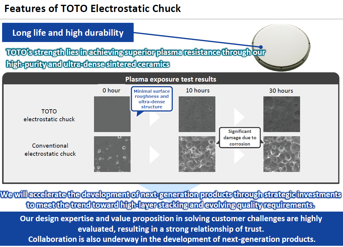
TOTO did not move into semiconductors simply because it knows how to make toilets. The real reason is its long-term accumulation of capabilities in ceramic powders, sintering, dimensional control, surface processing, and mass-production consistency. In its official ESC product descriptions, TOTO emphasizes high durability, low backside particle contamination on wafers, high-precision processing, and the ability to control wafer temperature according to customer requirements.
The ceramics used in semiconductor equipment are not ordinary ceramics. Ordinary ceramics may tolerate small amounts of impurities, minor surface defects, or slight batch-to-batch variation. But ceramics used in advanced process equipment cannot. A tiny particle, a small amount of surface wear, or a slight thermal non-uniformity can all become wafer defects.
ESCs Have Two Main Technical Routes: Coulomb and Johnsen-Rahbek
From the perspective of the adsorption mechanism, ESCs are generally divided into Coulomb-type and Johnsen-Rahbek-type designs. The main difference lies in the material properties of the dielectric layer and the way the clamping force is generated. The Coulomb type is closer to conventional capacitive attraction. The Johnsen-Rahbek type uses a dielectric material with a certain level of electrical resistance. When voltage is applied while the wafer is in contact with the chuck surface, a stronger adsorption effect is generated at the interface.

This may sound academic, but its industrial significance is very direct: different process temperatures, wafer backside conditions, material stacks, and plasma environments all require different ESC designs.
For example, thin wafers used in advanced packaging or after backside grinding may exhibit more severe warpage. High-aspect-ratio etching in 3D NAND may require stricter temperature uniformity and stronger plasma resistance. As wafers become thinner, structures become taller, and etching becomes deeper, the ESC is no longer just a “chuck.” It becomes part of the process control system.

Coulomb-type ESCs emphasize electrical stability and clean wafer release, while Johnsen-Rahbek-type ESCs emphasize stronger clamping force and better thermal contact, but require more sophisticated material and charge-control engineering.
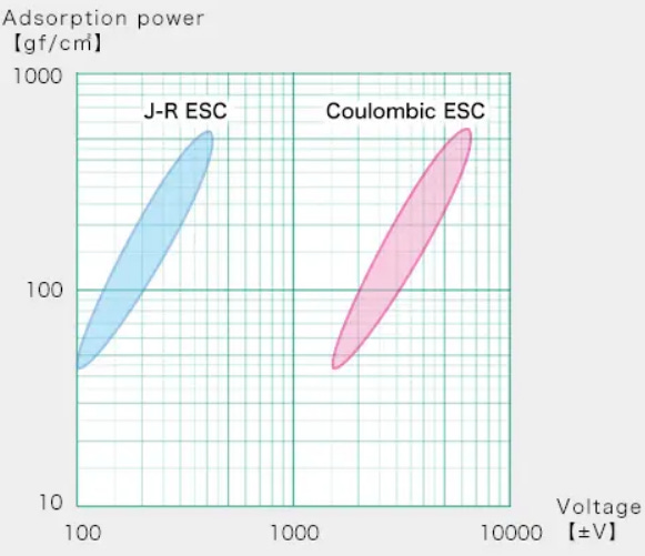
Adsorption power of J-R and Coulombic ESC / Source: TOTO
TOTO’s Greatest Strength Is Not Cross-Industry Expansion, but Long-Term Patience
TOTO’s semiconductor story is compelling not merely because of the contrast, but because it proves one thing: the real moat of a materials company is usually not built in one or two years.
TOTO’s Advanced Ceramics Division was established in 1984. This means the company did not suddenly transform itself after seeing the AI boom. Decades before AI became the center of attention, TOTO had already been investing resources into precision ceramics, materials development, process design, analysis and evaluation, and mass-production technologies.
There is a harsh reality in the materials industry: you cannot enter a wafer fab with a PowerPoint presentation.
What semiconductor customers care about is not storytelling. They care about long-term stability, batch-to-batch consistency, contamination control, failure modes, supply flexibility, and mass-production track records. For a material or component to be adopted in advanced process equipment, it usually has to go through a very long qualification cycle. This is also why many traditional materials companies, once they successfully enter the semiconductor supply chain, tend to form highly sticky customer relationships.
TOTO’s transformation is not a story of “a toilet company suddenly becoming an AI company.” It is a story of “a ceramics company spending decades waiting for semiconductor manufacturing to finally need the capabilities it had been best at all along.”
That is the real point of the story.
The Numbers Have Already Proved It: Semiconductor Ceramics Have Become TOTO’s High-Margin Growth Engine
The most convincing evidence is not the narrative, but the financial results.
TOTO’s financial results for the fiscal year ending March 2026 show that the company recorded total revenue of ¥737.4 billion and operating profit of ¥53.8 billion. Within this, New Business Domains — namely the Advanced Ceramics business — saw revenue increase from ¥50.3 billion in FY24 to ¥67.4 billion in FY25.
What matters even more is profitability.
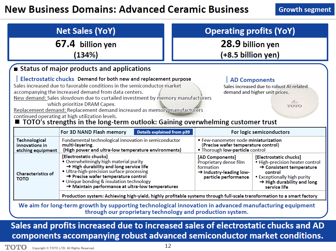
TOTO’s ceramics business reached revenue of ¥67.4 billion, operating profit of ¥29.0 billion, and an operating margin of 43% in FY25. The same data also shows that the sales mix of this business has become highly concentrated in semiconductors. In FY25, semiconductors accounted for 98% of the segment’s sales, a significant shift from 45% in FY09.
This means TOTO’s semiconductor materials business is no longer a small side business. It has become a high-profit, high-technology, high-supply-chain-value growth segment.
The meaning behind these figures is clear: TOTO did not “jump” from sanitary ware into semiconductors. Instead, it selected and concentrated its ceramics business over time, gradually shifting it almost entirely toward semiconductors.
Why Is AI Driving TOTO? The Answer Lies in Memory and Etching
AI is not only driving demand for GPUs.
AI servers require HBM, DRAM, NAND, SSDs, advanced logic chips, networking chips, and large-scale data center infrastructure. As data center demand rises, investment in memory and logic chip capacity is also pulled upward. Once fabs and equipment makers increase investment, the consumables, components, and key materials used inside semiconductor equipment also benefit.
In its financial presentation, TOTO clearly stated that the increase in electrostatic chuck sales was related to the semiconductor market environment driven by data center demand. AD components were also supported by robust AI-related demand and rising unit prices.
This is especially true for 3D NAND.

As the number of NAND layers continues to increase, etching depth, uniformity requirements, and equipment environments all become more demanding. TOTO’s materials show that as memory moves from 128 layers toward 300/400 layers, and potentially toward 1,000 layers in the future, the etching environment will become even more extreme. In this context, the durability of electrostatic chucks becomes an important competitive advantage. The company also mentioned cryogenic etching, or low-temperature etching, as an important technology for next-generation multilayer semiconductor manufacturing.

This is why TOTO’s story has suddenly been re-rated by the market.
In the past, investors looked at TOTO as a Japanese sanitary ware, housing equipment, Washlet, and market-penetration story. Now the market is beginning to realize that TOTO is also a key materials and equipment-component company within the AI memory supply chain.
The Real Moat: The “Narrow Gate” Business of Japanese Materials Companies
TOTO’s case also reveals one of the greatest strengths of Japan’s semiconductor supply chain: not every company needs to make the final product. Instead, many companies occupy extremely narrow, deep, and difficult-to-replace segments.
TOTO’s presentation shows that in the 2025 electrostatic chuck market, Japanese companies together held more than 97% global market share by shipment volume, while TOTO was the world’s second-largest supplier.

This is a typical Japanese supply-chain structure: the market may not be the largest, but concentration is high, process barriers are high, and customer qualification cycles are long. Once a company secures a position, it is very difficult to replace quickly.
This type of business has several characteristics.
First, the product is highly niche, but the cost of failure is extremely high.
Second, customers do not switch suppliers easily, because changing materials means restarting the qualification process.
Third, demand comes not only from new equipment, but also from replacement demand. TOTO noted that as the number of memory semiconductor layers increases, chamber environments become harsher, driving more frequent component replacement. At the same time, investment in new equipment and higher equipment utilization rates also support demand for both new parts and replacement parts.
Fourth, product value rises as process difficulty increases. The more advanced the process, the more it requires materials capabilities such as high purity, low particle generation, plasma resistance, precise thermal control, and high reliability.
This is the most fascinating aspect of semiconductor materials: they do not make money from traffic. They make money from “not being allowed to fail.”
TOTO’s Next Step: Not Just Riding the AI Tailwind, but Expanding Capacity and Reinvesting in R&D
TOTO also understands that this market cannot be sustained simply by relying on past technological dividends.
According to the company’s latest presentation, TOTO plans to continue investing in new product development and production capacity, supporting the growth of the semiconductor industry through “Quality and Uniformity.” Major related investments include approximately ¥30 billion to strengthen R&D and mass-production capabilities, ¥6 billion for an R&D prototype line, phased expansion of ESC capacity, and investment projects such as the Nakatsu No. 4 Plant.

There is one key point here: TOTO’s growth is not just the result of a sudden improvement in the market. The company has already entered a reinforcing cycle of capacity, R&D, and customer demand.
What do semiconductor materials companies fear most? It is not a lack of demand. It is demand arriving before they have capacity, qualification, and quality consistency in place. What TOTO is doing now is turning decades of accumulated materials capability into a larger-scale, higher-yield, and faster-development mass-production system.
This is consistent with the broader theme of the AI supply chain: the real bottleneck is not only chip design, but whether the entire supply chain can scale reliably.
What TOTO Means for Taiwan: Semiconductor Opportunities Are Not Limited to Fabs
TOTO’s story offers important lessons for Taiwan.
Taiwan is strong in foundry manufacturing, packaging and testing, IC design, server systems, and the PCB supply chain. But the next stage of competition will extend further into materials, equipment components, specialty chemicals, precision ceramics, thermal management, power delivery, inspection, and process-support materials.
A toilet company can become a semiconductor materials company. The key is not that it knows how to make toilets, but that it pushed its ceramic materials capabilities to the extreme.
The same logic applies to many traditional industries in Taiwan. Chemicals, ceramics, glass fiber, adhesives, precision machining, surface treatment, specialty coating, molding materials, films, inspection fixtures — as long as they can address real pain points in semiconductor processes, they all have the potential to evolve from traditional industries into part of the AI supply chain.

6月22日
Conclusion: In the AI Era, the Most Valuable Things Do Not Always Look Like AI
TOTO’s transformation story attracts attention because of its contrast.
A company moving from toilets to semiconductors sounds like a clickbait headline. But what is truly worth studying is not the contrast itself, but the industrial logic behind it.
In the AI era, the market will keep rediscovering hidden beneficiaries across the supply chain. Companies that were once viewed as mature, low-growth, or traditional manufacturers may be revalued if they control critical materials, equipment components, or process capabilities.

TOTO tells us one thing:
The semiconductor industry is not only about chip companies.
The AI supply chain is not only about GPUs.
The real moat is often hidden in materials, ceramics, consumables, equipment chambers, and even inside a century-old company that appears to make only toilets.
From toilets to semiconductors, TOTO did not take a cross-industry shortcut. It walked a decades-long path through the deep waters of materials engineering.

This is also the most formidable aspect of Japanese manufacturing: it may not always stand at the center of the stage, but when processes are pushed to their limits, the world suddenly realizes that certain critical components have long been in its hands.
6月16日
Thanks for reading SEMIVISION @_@! This post is public so feel free to share it.


PreviousNext