Japan’s Strategic Position in the Semiconductor Industry in the AI Era
Japan’s Strategic Position in the Semiconductor Industry in the AI Era
- Source: SemiVision
- Author: SEMIVISION
- Published: 2026-06-16T23:41:20+08:00
- URL: https://tspasemiconductor.substack.com/p/japans-strategic-position-in-the (1) Japan’s Strategic Position in the Semiconductor Industry in the AI Era


Japan’s Strategic Position in the Semiconductor Industry in the AI Era
Origianl Article By SemiVision Research [Reading time: 46 mins]

Jun 16, 2026
∙ Paid
Japan’s Strategic Position in the Semiconductor Industry in the AI Era
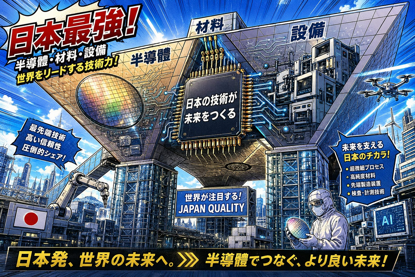
The History and Overall Positioning of Japan’s Semiconductor Industry
Japan is an important participant in the global semiconductor industry. After reaching its peak in the 1980s and facing competitive pressure after the 1990s, Japan still maintains extremely strong technological advantages in specialized fields today. In particular, Japanese companies hold world-class market shares in semiconductor manufacturing equipment, materials, testing and inspection, power devices, and automotive electronics.
With the rapid growth of artificial intelligence (AI), the Internet of Things (IoT), autonomous driving, cloud computing, and high-performance computing (HPC), the role of Japanese companies has further deepened. This report classifies these companies into five major functional categories:
Strategic Fab Equipment Leaders: including Tokyo Electron, SCREEN Holdings, and Kokusai Electric, which control key technologies in front-end wafer fabrication equipment.
AI Test, Inspection & Yield Control: including Advantest, Lasertec, and Tokyo Seimitsu / Accretech, which are responsible for post-fabrication testing and inspection to ensure chip quality and yield.
Wafer Materials & Ultra-Precision Processing: SUMCO provides silicon wafers, while DISCO supplies dicing, grinding, and polishing equipment, supporting the foundation of chip manufacturing.
Automotive, Power & Specialty Semiconductors: including Renesas Electronics and ROHM, focusing on automotive MCUs, power semiconductors, and silicon carbide (SiC) products.
Advanced Packaging & 3DFabric Ecosystem: including IBIDEN, Shinko Electric, Kyocera, Murata Manufacturing, Resonac, TDK, and Taiyo Yuden, focusing on IC package substrates, passive components, packaging materials, and advanced packaging solutions.
Through the above classification, SemiVision will provide a detailed analysis of each company’s technological strengths, product portfolio, market positioning, and its role and future development within the AI industry.
Core Conclusion: Japan May Not Produce the Most AI GPUs, but It Controls Many Critical Links That Make AI Chips Manufacturable
Global discussions around the AI semiconductor industry usually focus on NVIDIA, AMD, Broadcom, Google, Amazon, Microsoft, TSMC, Samsung Electronics, and SK hynix. However, when viewed from the perspectives of manufacturing equipment, silicon wafers, photomask inspection, wafer cleaning, thin-film deposition, grinding and dicing, testing, package substrates, electronic materials, MLCCs, magnetic components, and power semiconductors, the influence of Japanese companies is far greater than the visibility of end-chip brands alone would suggest.

Japan’s core advantages in the AI semiconductor era can be summarized in five areas:
It controls equipment and process modules that are difficult to replace in advanced manufacturing.
It possesses manufacturing control capabilities related to yield, contamination, dimensional accuracy, defect management, and testing.
It controls foundational materials and precision processing technologies, including silicon wafers, packaging materials, grinding and dicing consumables.
It provides critical components for AI server power delivery, passive components, and power conversion.
It is a major indirect beneficiary of advanced packaging, HBM, chiplets, and high-power AI systems.
Therefore, Japan’s role in AI semiconductors should not be understood simply as whether Japan has an AI GPU company comparable to NVIDIA. Rather, it should be understood as follows:
Japanese companies control many key nodes in AI chip manufacturing that require high precision, high cleanliness, high reliability, high material barriers, and high yield.
As AI chips evolve from single large SoCs toward chiplets, HBM, 2.5D/3D packaging, hybrid bonding, glass-core substrates, high-density substrates, and more complex power delivery networks, the importance of Japanese suppliers will not decline. On the contrary, it may increase as system complexity continues to rise.

2月6日
Structural Changes Driven by AI Semiconductors
To understand the opportunities for these Japanese companies, we must first understand how AI chips differ from traditional semiconductors.
AI Chips Are Not Simply About “More Transistors”
The growth of AI GPUs, ASICs, and high-performance computing chips is simultaneously driving the following changes:
Larger logic die area;
Higher transistor counts;
More HBM stacks;
Higher I/O count and speed;
Larger package size;
Higher chip power consumption;
Longer test time;
Higher defect cost;
More severe wafer and package warpage;
Greater challenges in power integrity and thermal management.
As a result, the value of AI semiconductors is no longer concentrated only in chip design and wafer foundry manufacturing. It is spreading across equipment, materials, testing, and packaging.
For example, if a high-end AI accelerator includes:
One or multiple logic compute dies;
Eight or more HBM stacks;
A silicon interposer or RDL interposer;
A large ABF substrate;
Tens of thousands of microbumps and C4 bumps;
A large number of MLCCs, inductors, and power delivery components;
then even a small localized defect could cause the entire high-value package to fail.
This raises the importance of cleaning, inspection, testing, thinning, dicing, packaging materials, and power components.
How AI Changes Yield Economics
For traditional low-cost chips, a defect may result in the loss of only a component worth a few dollars or a few dozen dollars.
But if a large AI package fails during back-end testing, the loss may include:
Advanced-node logic dies;
Multiple HBM stacks;
The interposer;
The ABF substrate;
Packaging materials;
Long equipment capacity time;
Testing and assembly costs.
Therefore, the more expensive AI chips become, the greater the need for:
Earlier testing;
More extensive testing;
More precise defect inspection;
Known Good Die;
More complete wafer sort;
Stricter process monitoring;
Better material traceability and statistical process control.

2025年8月25日
This is exactly where the value of companies such as Advantest, Lasertec, Tokyo Seimitsu (Accretech), SCREEN, Tokyo Electron, and DISCO comes from.

Overview of Japan’s AI Semiconductor Supply Chain
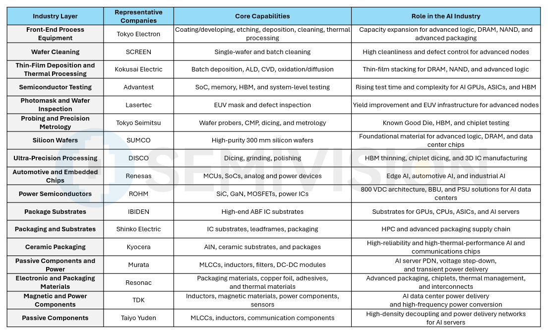
Below, we will share the latest updates and introductions for all the companies listed in the table.
Front-End Process Equipment: Japan’s Most Critical Semiconductor Strategic Asset
Japan holds a significant global market share in wafer fabrication equipment and can provide the etching, deposition, cleaning, bonding, and thermal processing equipment required for front-end manufacturing processes. This section will introduce how companies such as Tokyo Electron, SCREEN, and Kokusai Electric support the demands of AI and advanced process technologies through continuous technological innovation.
Tokyo Electron (TEL) : Japan’s Most Comprehensive Front-End Equipment Platform
Company Overview
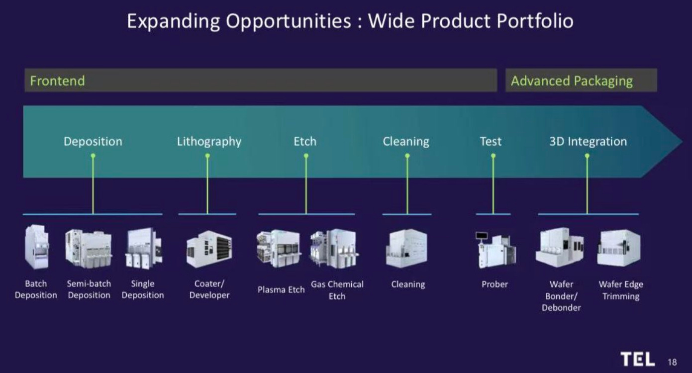
Tokyo Electron, founded in 1963, is the world’s third-largest supplier of semiconductor manufacturing equipment. Its product portfolio spans front-end process equipment, including thin-film deposition, etching, thermal processing, and photoresist coating; back-end packaging equipment for 3D integration; and display manufacturing equipment.
In the AI era, TEL’s strength lies in its ability to provide both front-end wafer process equipment and back-end 3D integration technologies, helping shorten the distance between memory and computing units while improving performance.
According to TEL’s official blog, the AI semiconductor market is expected to grow at a compound annual growth rate of 30% through 2028. To address this trend, TEL continues to innovate in 3D integration, or 3DI, equipment and digital twin models.
3D Integration Equipment and Digital Twins
3D integration technology enables multiple chips, or chips and wafers, to be stacked into a single device, bringing logic and memory closer together to reduce latency. It combines front-end and back-end processes, including wafer bonding, temporary bonding and debonding, edge trimming, and laser debonding.
TEL’s product lineup includes:
•Synapse™ Si: a wafer bonding system that precisely bonds two wafers together.
•Synapse™ V and Z Plus: temporary bonding and debonding systems that help temporarily fix chips in place during stacking.
•Ulucus™ L: an edge trimming system that processes wafer edges to improve yield.
•Ulucus™ LX: an extreme laser debonding system used to separate chips from carriers.

TEL uses digital twin technology to build process models and combines physics-based machine learning to predict material behavior during development and process optimization. This helps reduce the number of physical trial runs and address issues such as wafer warpage and post-bonding distortion.
In its sustainability report, TEL also mentioned its research and development of neuromorphic devices and resistive memories, aiming to mimic human brain computing and shorten the distance between memory and logic devices.
Through tools such as generative AI, TEL also applies AI in process development to simulate parameters and predict output, demonstrating its active positioning in the AI field.
Investment in AI, Advanced Logic, and Memory
As generative AI, edge computing, and high-performance computing become more widespread, demand for AI accelerators, CPUs, GPUs, and memory is surging, driving investment in advanced process technologies.
TEL places strong emphasis on the AI market. Through its 3D integration equipment and front-end deposition and etching tools, the company supports process nodes below 5 nm.
In addition, TEL is developing analog neural network devices that convert electrical resistance into components capable of mimicking synaptic behavior, exploring low-power AI computing.
TEL’s AI applications are not limited to the equipment itself. They also include the use of AI and machine learning to optimize processes and improve energy efficiency.
Future Outlook
Over the next several years, demand for AI servers and memory bandwidth will drive more companies to adopt 2.5D / 3D packaging and advanced process technologies.
TEL has comprehensive front-end and back-end integration capabilities. Together with strategic investments and collaboration with customers such as TSMC, Samsung, and Intel, the company is expected to continue leading this field.
In decarbonization and sustainability, TEL is also committed to reducing chemical and energy consumption. Through highly efficient equipment design and green innovation, the company is aligning itself with the global net-zero trend.

SCREEN: The More Advanced AI Processes Become, the More Critical Cleaning Becomes
SCREEN’s core strength in semiconductors lies in wafer cleaning equipment.
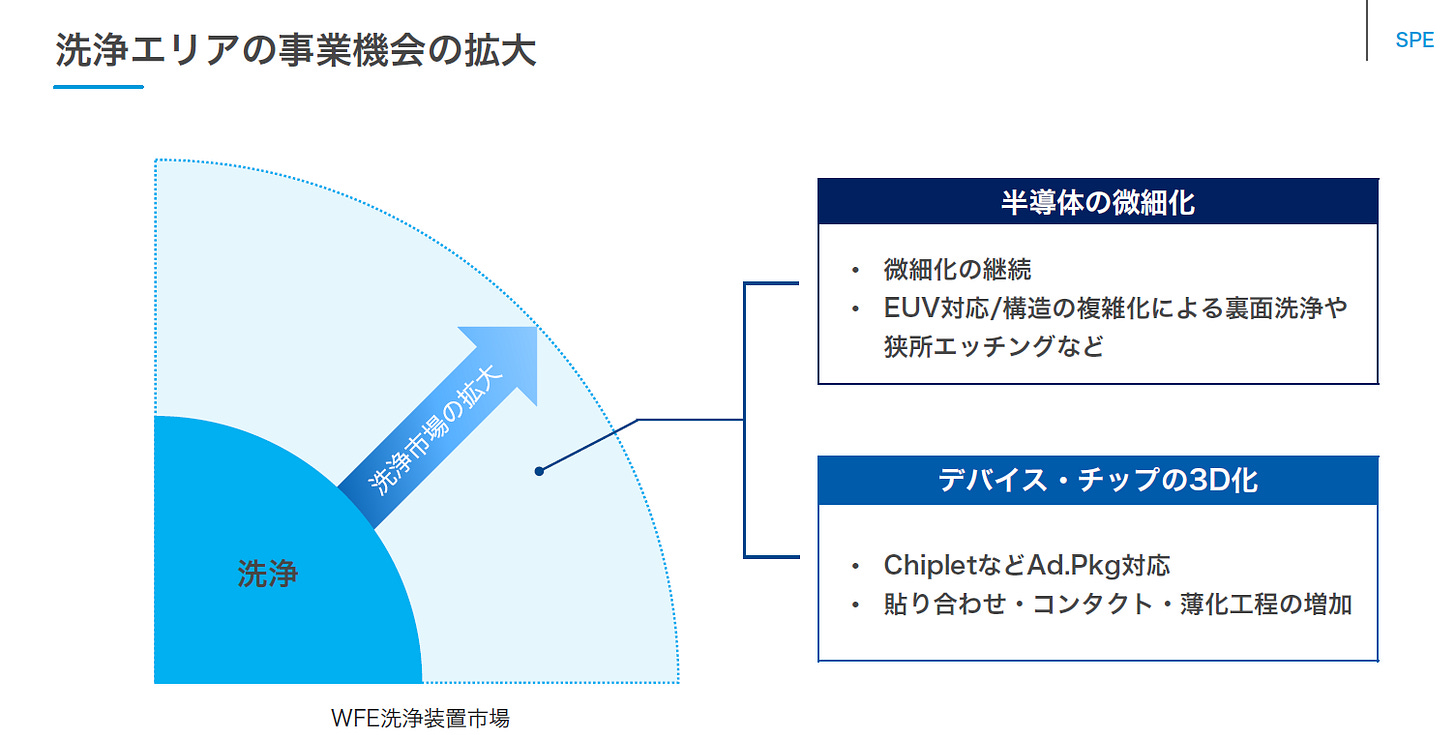
Cleaning may appear less attention-grabbing than lithography, etching, or deposition, but in advanced nodes, any particle, metal contamination, or organic residue can lead to:
Open circuits;
Short circuits;
Increased contact resistance;
Leakage;
Poor film adhesion;
Hybrid bonding voids;
Yield loss.
Therefore, as the number of advanced process steps increases, the number of cleaning steps usually rises as well.
In recent years, SCREEN has continued to expand its R&D and overseas process development capabilities, including the establishment of related R&D facilities in Albany, New York. This indicates that its strategy is to participate earlier in advanced-node process definition, rather than simply supplying equipment after fabs enter mass production.
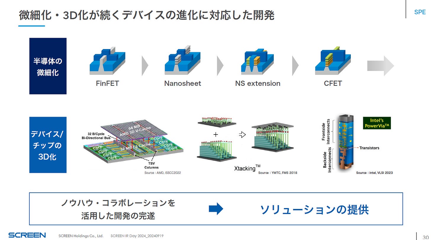
Company Overview
SCREEN Holdings is a Japanese semiconductor and display equipment company with origins dating back to 1943. Today, it mainly provides wafer cleaning systems, image processing technologies, printing and display equipment, and imaging solutions.
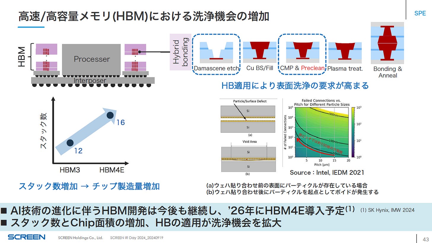
Cleaning is an indispensable step in front-end semiconductor manufacturing. As process nodes shrink to 5 nm, 3 nm, and beyond, any particle contamination can lead to yield loss. As a result, demand for cleaning and contamination control has become increasingly stringent.
Advanced Wafer Cleaning Technology
In its press release, SCREEN introduced its SU 3400 single-wafer cleaning system, emphasizing that process miniaturization has made logic and memory chips more sensitive to particles.
The SU 3400 highlights high throughput, with the ability to process up to 1,200 wafers per hour, as well as reduced environmental impact. By shrinking the cleaning chamber, improving chemical circulation, and reducing chemical usage, the system achieves both high productivity and better environmental performance.
The company continues to use IoT-based support systems to monitor equipment conditions and enable predictive maintenance, while also reducing consumables and emissions.
Another report mentioned that SCREEN’s SU 3200 and SU 3300 systems received the Green Value Award because they reduce chemical and water usage by optimizing chemical temperature and cleaning methods, thereby improving customers’ cost of ownership, or CoO.
As chip dimensions shrink, the chemicals required to remove particles typically increase. However, SCREEN’s technology can reduce chemical consumption without sacrificing cleaning performance, demonstrating its strategy of balancing sustainability and economic efficiency.
AI and Advanced Process Demand
Demand for AI and high-end computing is driving process technologies toward 2 nm and even smaller nodes, which also raises the requirements for wafer cleaning.
Because AI chips contain a large number of metal layers and high-density structures, even tiny particles or organic contamination can affect performance. SCREEN continues to develop higher-efficiency cleaning equipment, including solutions that support EUV mask washing and cleaning.
Its production systems combine high performance with energy efficiency, meeting customers’ dual requirements for cost reduction and environmental sustainability.
Kokusai Electric: A Batch Deposition Specialist in the Era of Thin-Film Stacking
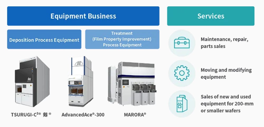
Kokusai Electric’s core strength lies in thin-film deposition and processing, especially for high-aspect-ratio structures such as DRAM capacitors, 3D NAND memory cells, and vias in advanced logic chips.
Official documents indicate that as the expansion of AI and 5G drives semiconductor market growth, demand for 3D structures and increasingly complex device architectures is rising. This makes thin-film deposition and film quality improvement more difficult.
In response, Kokusai Electric has developed nanoscale deposition technologies and batch ALD, enabling the formation of high-quality thin films while maintaining high productivity.
Kokusai Electric mainly focuses on:
Batch CVD;
ALD;
Oxidation;
Diffusion;
Thermal processing;
Thin-film modification.

Its competitiveness does not come from the breadth of its product portfolio, but from its batch-processing capabilities:
High throughput;
High uniformity;
Low cost;
Simultaneous processing of multiple wafers;
Control over film thickness and material quality.
Kokusai officially positions itself in the fields of deposition and thin-film processing that directly affect semiconductor performance.
Kokusai’s Relationship with AI
Kokusai Electric’s core strength lies in thin-film deposition and processing, especially for high-aspect-ratio structures such as DRAM capacitors, 3D NAND memory cells, and vias in advanced logic chips.
Official documents indicate that as the expansion of AI and 5G drives semiconductor market growth, demand for 3D structures and increasingly complex device architectures is rising. This makes thin-film deposition and film quality improvement more difficult.
In response, Kokusai Electric has developed nanoscale deposition technologies and batch ALD, enabling the formation of high-quality thin films while maintaining high productivity.
DRAM and HBM
HBM is essentially a stack of high-performance DRAM.
In DRAM manufacturing, capacitor structures, dielectric layers, electrodes, contacts, and insulating layers require extensive deposition and thermal processing.
As DRAM capacitor structures become taller and deeper, the importance of ALD increases, because ALD can form more uniform films inside high-aspect-ratio structures.
NAND
Although NAND and AI accelerators are not exactly the same market, AI data centers still require massive storage capacity.
As the number of 3D NAND layers increases, it drives demand for:
High-aspect-ratio etching;
Multi-layer thin-film deposition;
Batch film formation;
Thermal processing.
GAA and Future Logic
GAA transistors require precise control over multiple Si/SiGe layers, dielectric layers, and metal layers.
If Kokusai can further improve its material control capabilities in both single-wafer and batch ALD, it may expand its exposure to logic manufacturing.
Future Technologies
The computing density required by AI servers demands chips with higher speed and thin films that help reduce leakage current.
Kokusai Electric’s ALD technology can provide high-k dielectric materials, metal gates, and isolation layers at extremely thin thicknesses, supporting technologies such as FinFET, GAA, or gate-all-around transistors, and 3D NAND.
The company is also working to introduce intelligent monitoring and AI-based equipment management into manufacturing processes, enabling predictive equipment status analysis, yield improvement, and energy-efficiency optimization.

AI Test, Inspection, and Yield Control: A New Field Driven by Increasing Chip Complexity
As chip architectures evolve toward multi-chip designs, chiplets, high-performance SoCs, and HBM memory, both test volume and test complexity are increasing significantly. The following companies provide essential test and inspection solutions for the AI era.

2025年8月20日
Advantest: The Higher the Complexity of AI Chips, the Greater the Value of Testing
Advantest is the world’s largest supplier of semiconductor test equipment, providing automated test equipment, or ATE, burn-in systems, and test solutions. Its customers span logic chips, memory, RF devices, automotive electronics, and other semiconductor markets.
In response to trends such as AI and HPC, Advantest has developed test platforms for high-end SoCs, GPUs, AI accelerators, and HBM.
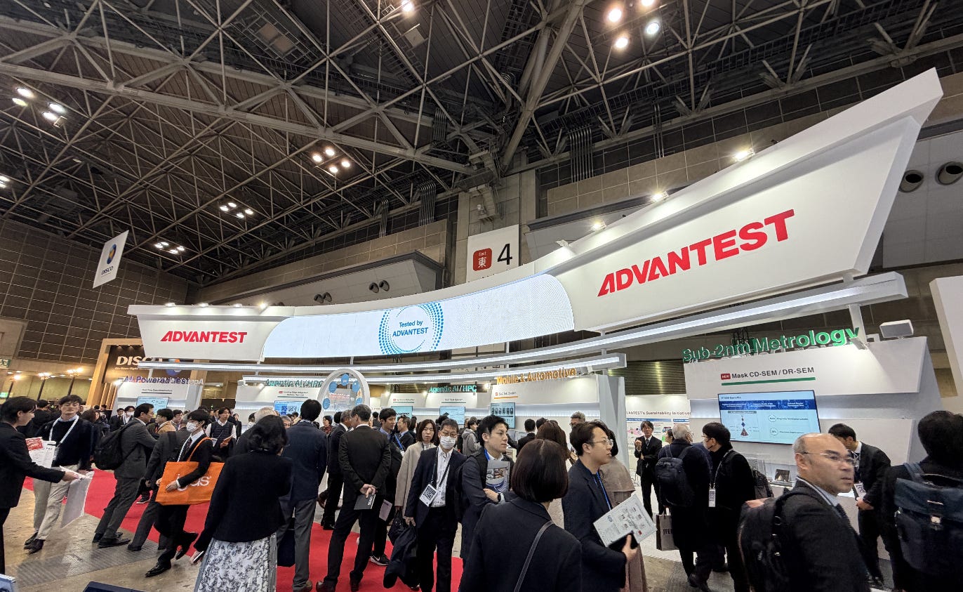
Its product portfolio covers:
SoC testing;
Memory testing;
HBM testing;
Handlers;
System-level testing;
Measurement and data analytics.
Advantest has clearly stated that demand for AI and HPC devices is driving stronger demand for semiconductor testing. Its memory test solutions also cover next-generation products such as HBM, GDDR7, LPDDR6, and DDR6.
Why Do AI Chips Require More ATE?
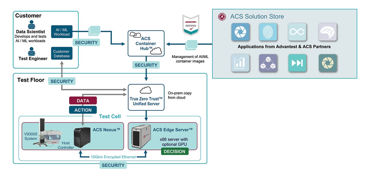
In 2025, Advantest collaborated with NVIDIA to launch Advantest Cloud Solutions Real-Time Data Infrastructure, or ACS RTDI, which uses GPU acceleration for real-time AI analytics.
According to the official announcement, the system can train multiple models simultaneously and detect anomalies in real time from the massive data streams generated by each chip. This transforms testing from a traditional validation task into an AI-driven adaptive process.
ACS RTDI can reduce latency, lower power consumption, and save costs. It has been applied to NVIDIA’s Blackwell and next-generation products, marking a new stage for AI-driven semiconductor testing.
Larger Die Size
As chip area increases, the potential number of defects also rises, which in turn increases the number of test patterns required.
Higher I/O Speeds
AI GPUs and ASICs involve:
HBM interfaces;
PCIe 6.0;
CXL;
224G SerDes;
NVLink-like high-speed interfaces;
Multi-die die-to-die interconnects.
These interfaces require higher bandwidth, lower jitter, and more precise timing-margin testing.
Higher Power Consumption
Testing high-power chips is not simply about applying input vectors and reading outputs. It also requires handling:
High current;
Transient current;
Temperature control;
Thermal management;
Socket contact;
Power droop;
Thermal throttling.
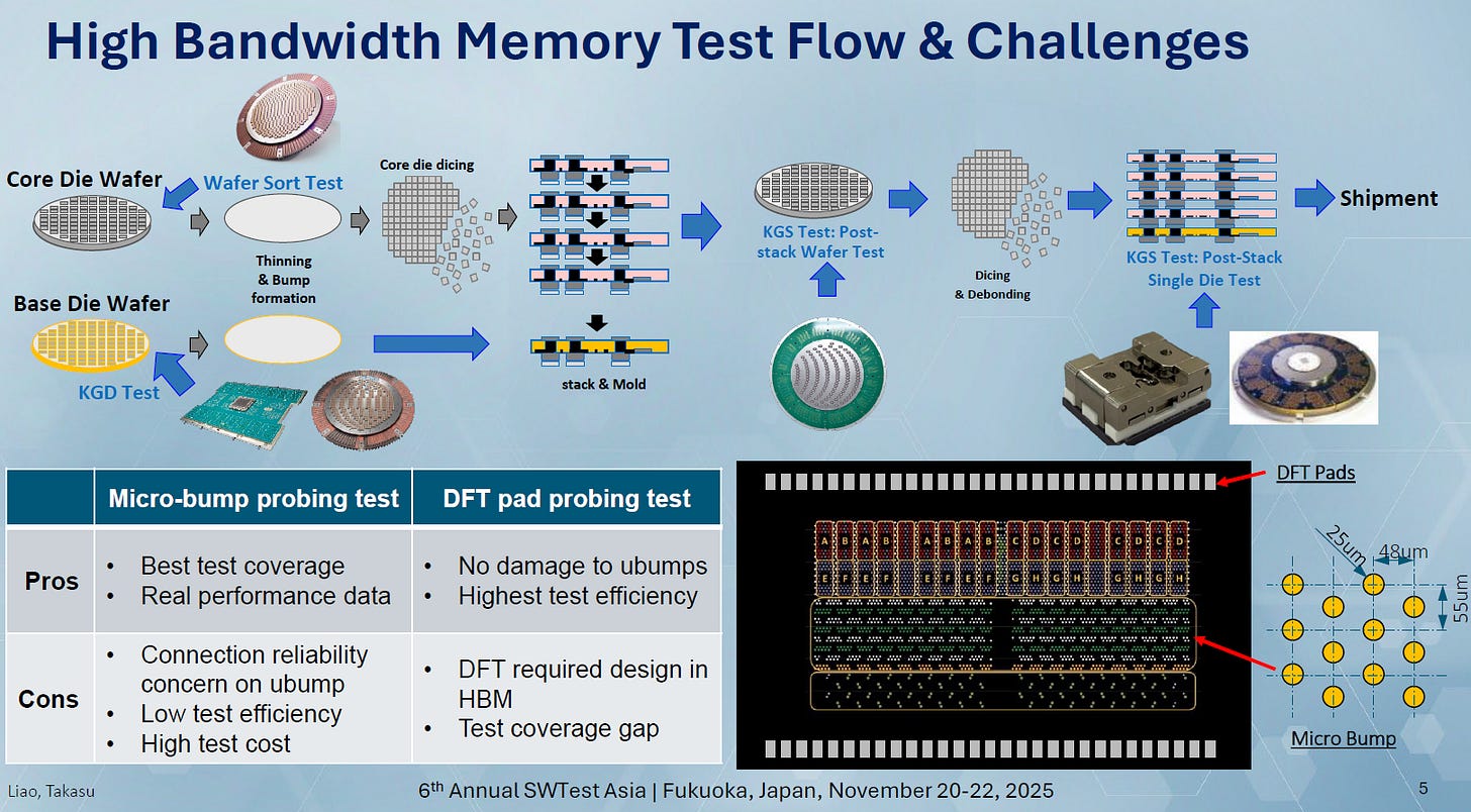
HBM Testing
HBM is built by stacking multiple DRAM dies.
Testing may cover:
DRAM dies;
Known Good Die;
Base die;
TSVs;
Micro-bumps;
Post-stack testing;
Testing after integration with GPUs.
Therefore, HBM does not merely add another memory tester. It increases the complexity of the entire test chain.
Chiplets
In a chiplet architecture, a single defective die can compromise the entire package. As a result, pre-bond test coverage must be increased.
Advantest’s Role in AI

Advantest’s technical presentations indicate that HPC and AI devices are typically composed of processor dies, I/O dies, and high-bandwidth memory, or HBM.
Over the next five years, the number of transistors is expected to increase fivefold, meaning that test volume will also grow exponentially. As chip size increases and structures become more complex, test procedures must cover both pre-package and post-package testing, while also managing thermal and power constraints.
Test content includes scan testing, built-in self-test, or BIST, stress testing, and power testing. These requirements place strict demands on test platform performance, channel count, and thermal design.
Advantest is not merely a test equipment supplier. It is a “loss controller” in the yield economics of AI chips.
Its value lies in identifying issues early, including:
Logic defects;
Memory errors;
High-speed interface issues;
Power integrity abnormalities;
Thermal problems;
Package interconnect defects.
In 2026, the company continues to showcase testing innovations for AI and HPC, reflecting that its products have evolved from traditional mass-production testing tools into a comprehensive high-performance device testing platform.
Future Technology Directions
In the AI field, Advantest uses AI-driven test management software and large-scale data analytics to predict and optimize production-line yield.
The company continues to invest in ATE systems that support chiplets, 2.5D / 3D packaging, and HBM, while also working with semiconductor design companies to introduce design-for-testability, or DFT, specifications.
As AI model sizes continue to expand rapidly, test demand will keep rising. Advantest’s scalable platforms and cloud-based solutions are expected to play a critical role.

2025年8月10日
Lasertec: The Mask Defect Gatekeeper in the EUV Era
Lasertec is a company specializing in semiconductor and optical inspection equipment, and is particularly well known for its EUV mask inspection systems. EUV, or extreme ultraviolet lithography, is a core technology for enabling 5 nm and smaller process nodes, and the quality of EUV masks directly affects wafer yield.
Lasertec’s strategic value comes from its inspection capabilities for advanced photomasks and EUV-related applications.
Unlike conventional transmissive photomasks, EUV masks use a reflective multilayer structure.
Defects may exist in:
Multilayer films;
Absorbers;
Mask blanks;
Pellicles;
Pattern surfaces;
Buried defects.
At advanced nodes, mask defects can be replicated across a large number of wafers. Therefore, photomask inspection carries significant leverage in yield control.
EUV Mask Inspection and Microscopy Technology
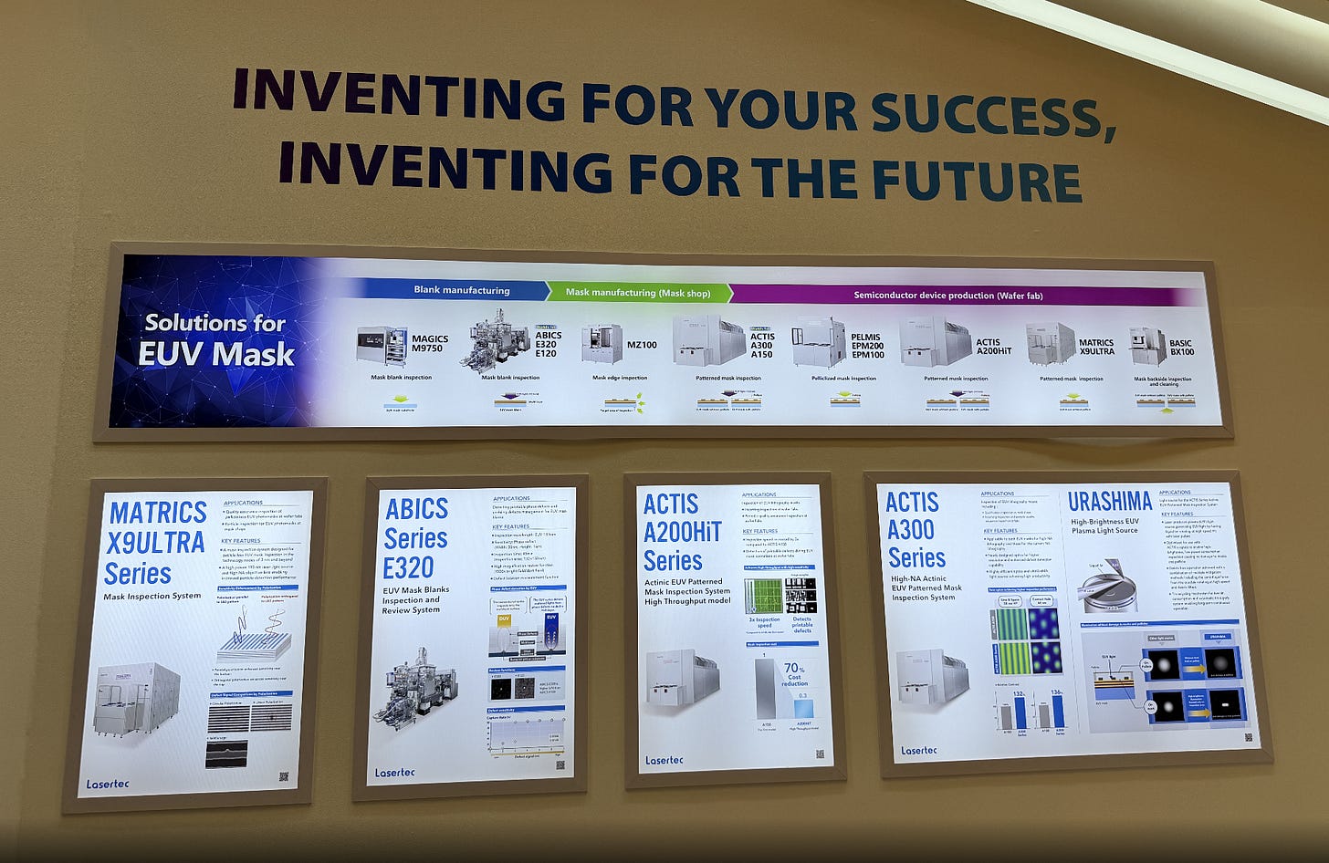
Lasertec states on its website that the company began developing EUV mask inspection systems at an early stage and has now launched six related products.
Since 2019, major chip manufacturers have begun using lithography based on the 13.5 nm EUV wavelength to produce 5 nm and even smaller patterns, supporting innovations such as 5G and AI.
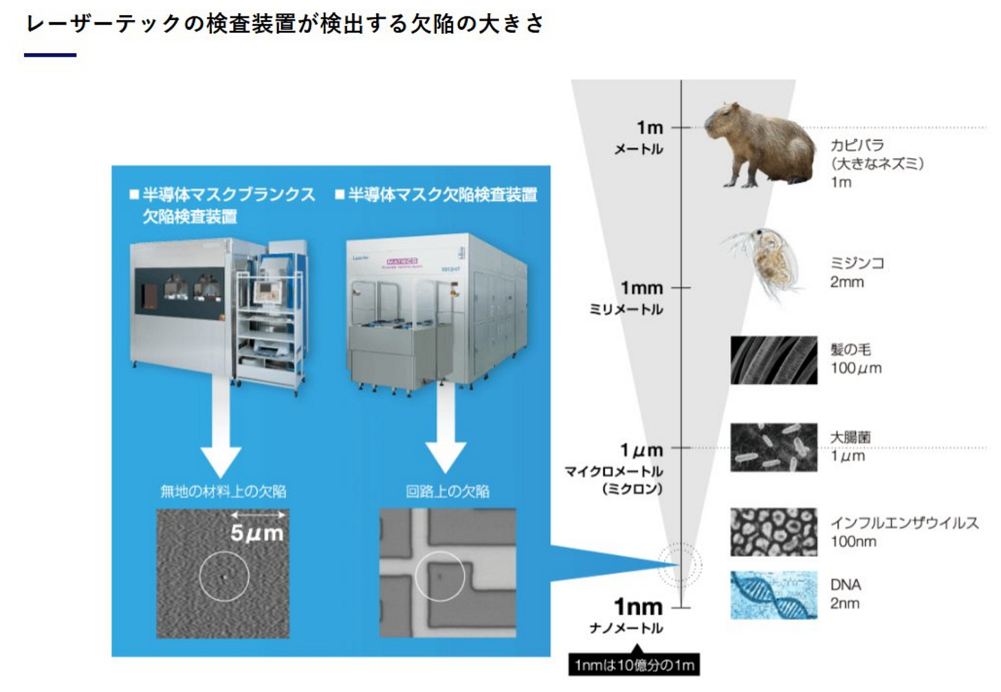
As line widths continue to shrink, defects on masks must be detected through high-resolution scanning. Lasertec’s systems use highly integrated optics and algorithms to locate tiny defects, helping prevent production line disruptions.
Lasertec’s Role in AI
The AI market requires the most advanced process technologies, and EUV is a key enabler for GAA FETs and dense interconnect routing.
Lasertec’s inspection systems can be used for EUV mask inspection, EUV blank inspection, and metrology, helping fabs eliminate defects before mass production.
Looking ahead, as High-NA EUV lithography is adopted and sub-2 nm technologies emerge, Lasertec is expected to continue advancing higher-resolution inspection while incorporating AI analytical algorithms to improve inspection efficiency.
AI GPUs and ASICs are typically manufactured using advanced process nodes.
As a result, demand for AI chips indirectly drives demand for:
EUV mask volume;
Photomask inspection;
Mask blank inspection;
Actinic inspection;
High-NA EUV preparation.
Lasertec does not directly manufacture AI chips, but it serves as a core infrastructure provider for maintaining yield in advanced semiconductor manufacturing.
New Opportunities from High-NA EUV
High-NA EUV will improve resolution, but it also introduces new challenges, including:
Stricter mask defect control;
Anamorphic imaging;
More complex mask designs;
Higher overlay requirements;
A smaller process window.
As a result, both the precision of inspection equipment and the capability of inspection algorithms must continue to improve.
Future Development Directions
High-NA EUV mask inspection;
Higher-sensitivity actinic inspection;
Pellicle defect inspection;
AI-based defect classification;
Mask repair verification;
Correlation analysis between wafer defects and mask defects.
Risks
High product concentration;
Long equipment lead times;
Customer concentration among a small number of wafer fabs and mask suppliers;
Continued competitive investment from companies such as KLA.
Tokyo Seimitsu / ACCRETECH: From Probers to Metrology and Back-End Processing
Tokyo Seimitsu, under its Accretech brand, provides wafer probing systems and precision measurement equipment, holding an important position in the wafer probing market.

Tokyo Seimitsu, operating under the ACCRETECH brand, has two major business segments:
Semiconductor manufacturing equipment;
Precision measuring instruments.
Its semiconductor equipment portfolio includes:
Wafer probers;
Dicing machines;
Grinding equipment;
CMP-related equipment;
Back-end testing and assembly equipment.
The company regards probers as one of its core products, and its FY2026 materials also indicate growing demand for testing equipment such as probing machines.
Advanced Wafer Probers and Smart Functions
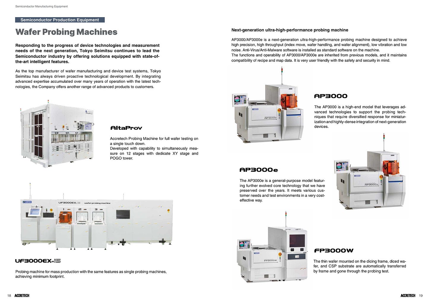
Tokyo Seimitsu’s company profile indicates that its high-end models, such as the AP3000 and AP3000e, feature high precision, high throughput, low vibration, and built-in antivirus software.
Through a dedicated XY stage and POGO tower, these systems can test 12 workstations simultaneously, supporting device miniaturization and high-density integration.
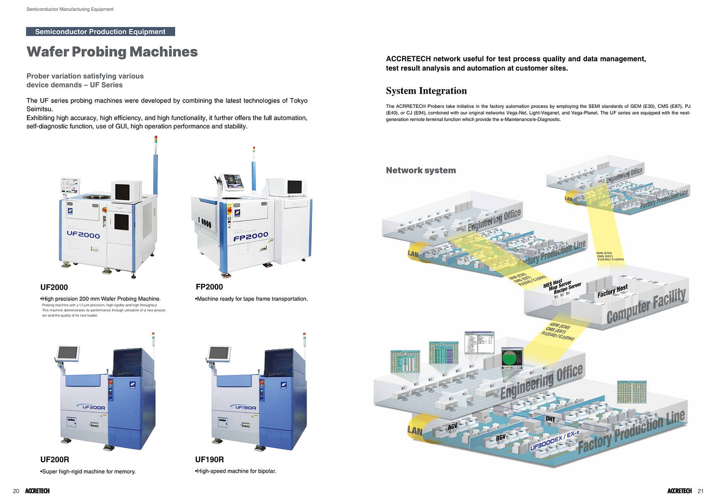
The UF series supports remote operation and maintenance based on SEMI standards, and also provides e-maintenance and e-diagnostic services, enabling smart factory operations and automated production.
These functions are particularly important for testing chiplets or complex SoCs, as they can reduce the need for human intervention and improve throughput.
AI-Driven Demand for Probers
As chiplet packaging and HBM adoption expand, wafer probers must handle larger interconnect modules and higher I/O density.
Tokyo Seimitsu is developing test platforms with AI-enabled functions, such as automatically correcting probe-to-die alignment through image recognition, using big data analytics to predict probe wear and yield, and combining robotic arms for automatic exchange.
In addition, wafer probers will become more closely integrated with design-for-testability, or DFT, at the chip design stage, enabling earlier defect prediction and elimination while improving production efficiency.

5月25日
Wafer Materials and Ultra-Precision Processing: The Foundation and the Cutting Edge
Semiconductors require high-quality silicon wafers and ultra-precision processing technologies to produce stable and reliable chips. Under the wave of high-speed AI computing, requirements for these materials and equipment have become even more stringent. This section introduces two companies: SUMCO and DISCO.

2025年9月16日
SUMCO: AI Chips Are Still Built on High-Quality Silicon Wafers
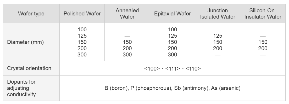
SUMCO is one of the world’s major silicon wafer suppliers, providing 300 mm, 200 mm, and smaller-diameter wafers for logic, memory, power, and automotive semiconductors.
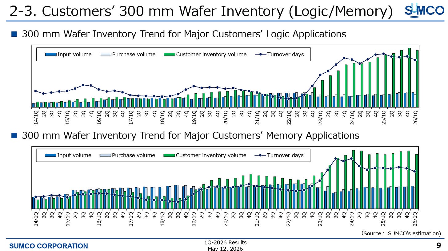
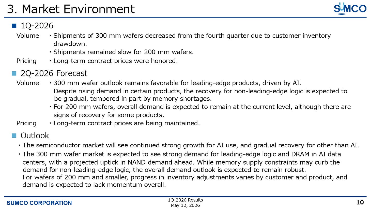
SUMCO’s management policy states that the silicon wafer market will continue to grow due to the expansion of data communications, generative AI, autonomous driving, digital transformation, and electric vehicles. Demand for 300 mm wafers is expected to continue increasing, while 200 mm wafer demand is expected to remain stable. The report also forecasts that NAND demand will increase along with the growth of server SSDs.

SUMCO is one of the world’s leading suppliers of semiconductor silicon wafers. Its core products include:
300 mm polished wafers;
Epitaxial wafers;
Annealed wafers;
Specialty wafers such as SOI;
High-precision wafers for advanced logic and memory applications.
Applications and Value of Silicon Wafers
SUMCO’s sustainability report details the broad applications of silicon wafers. In addition to computers, communication equipment, and data centers, silicon wafers also support automotive advanced driver assistance systems, or ADS, security cameras, smart meters, energy-saving devices, and train IGBTs.
Silicon wafers enable device miniaturization and support applications such as AI, robotics, and big data. They are also used in driver-assistance systems, electric-vehicle IGBTs, and renewable-energy power management.
This shows that SUMCO’s products are critical across multiple AI-driven fields, with demand spanning consumer electronics, automotive applications, and industrial control.
SUMCO’s 2025 business report indicates that AI data centers are driving demand for 300 mm wafers used in advanced logic and DRAM. The company has also previously invested in expanding capacity for high-precision 300 mm wafers.
Why Do Advanced AI Chips Require Better Wafers?
As process nodes continue to shrink, the following wafer parameters become increasingly important:
Flatness;
Nanoscale surface roughness;
Crystal defects;
Oxygen concentration;
Metal contamination;
Warpage;
Edge profile;
Resistivity uniformity.
In 2 nm, GAA, and future backside power delivery processes, both sides of the wafer may be involved in manufacturing steps, placing even higher requirements on flatness and mechanical stability.

Silicon wafer production takes place in three steps. SUMCO carries out each of these steps in clean rooms boasting the highest level of cleanliness. Applying the strictest quality control, we produce silicon wafers of exceptionally high purity and quality.
AI Demand for SUMCO Is Not Simply About Wafer Volume
AI GPU shipment volume may not necessarily match that of smartphone SoCs, but AI chips typically require:
The most advanced process nodes;
Higher-specification wafers;
Large die sizes;
More HBM DRAM wafers.
Therefore, AI’s impact on SUMCO may be reflected not only in volume, but also in:
A higher-end product mix;
Higher utilization of advanced 300 mm wafers;
Long-term contracts;
More stringent quality specifications.
Technology and Future Development
AI requires large volumes of advanced logic chips and memory, and 300 mm wafers are the foundation for these devices.
The company also values demand for smaller-diameter wafers below 150 mm, particularly in automotive and power devices, and is adjusting its capacity structure to optimize revenue.
Looking ahead, SUMCO will follow customer demand for 2 nm and more advanced process nodes by providing wafers with better flatness and thickness uniformity.
DISCO: A Specialist in Dicing, Grinding, and Polishing
DISCO is a globally recognized manufacturer of precision processing equipment, providing dicing saws, laser processing systems, grinding equipment, and polishing tools.
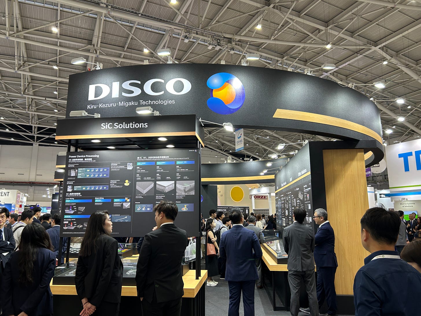
Its products are widely used for dicing logic chips, memory chips, power devices, and optoelectronic components.
DISCO’s main businesses also include maintenance, training, disassembly and recycling, equipment leasing, and the manufacturing of diamond abrasive tools.
DISCO’s core capabilities include:
Wafer dicing;
Wafer grinding;
Polishing;
Laser processing;
Blades;
Grinding wheels;
Dicing tape and related consumables;
Process know-how.
As AI chip packaging becomes increasingly complex, DISCO’s importance continues to rise.
Laser Saws and AI Chip Demand
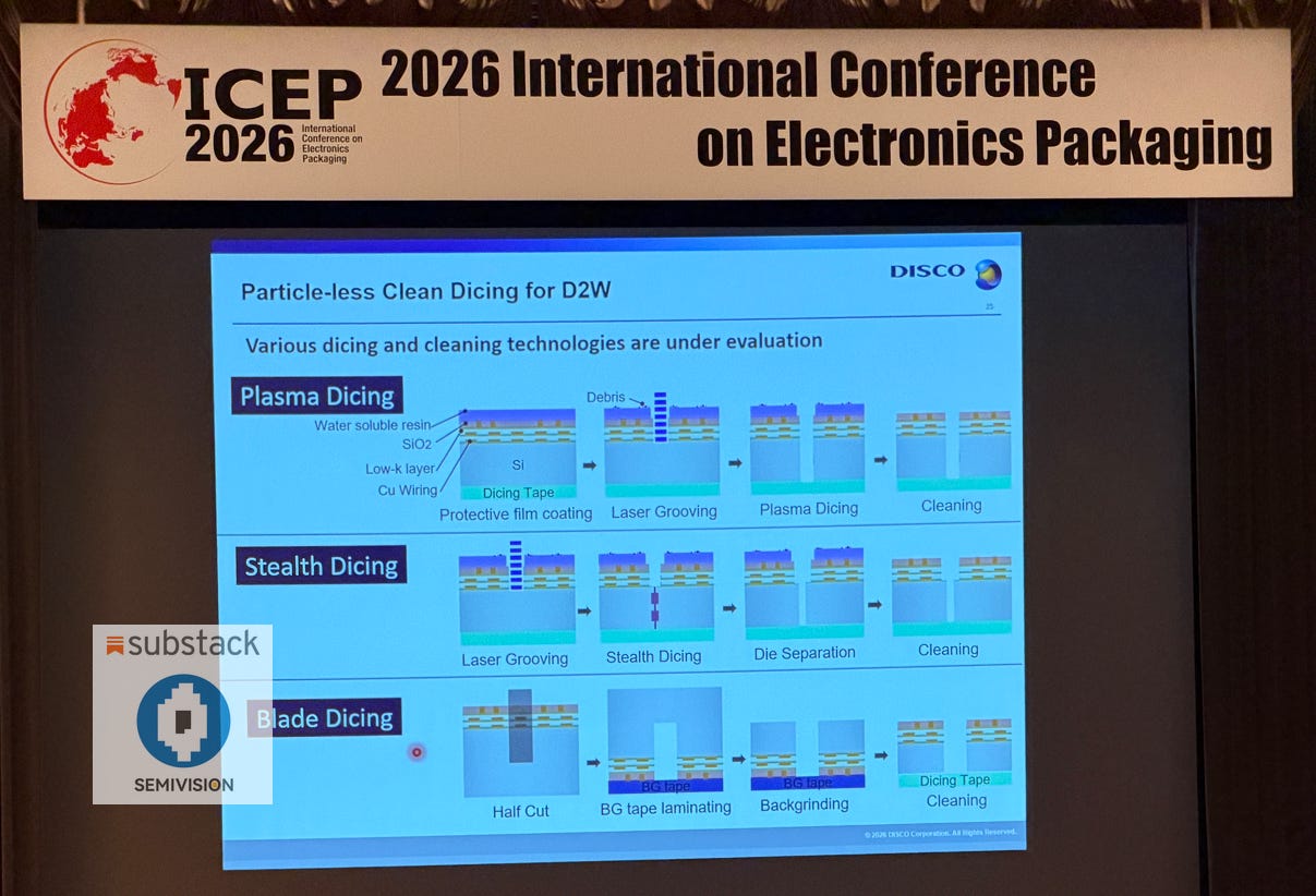
In a 2026 press release, DISCO stated that shipments of its laser saws have tripled since 2020, driven by the need for low-damage, high-precision processing in high-performance logic and high-density memory.
Laser saws are used for chip dicing, ultra-thin memory device processing, and SiC wafer manufacturing.
As demand for generative AI and high-performance memory increases, high-efficiency and low-damage dicing technologies have become indispensable.
DISCO’s technologies support ultra-thin chip processing and the singulation of chiplet modules, providing a foundation for advanced packaging.
Why Does HBM Need DISCO?
HBM requires DRAM dies to be thinned in order to reduce the overall stack height.
For example, as HBM stacks evolve from 8-Hi and 12-Hi toward 16-Hi or higher, the thickness of each die must be reduced.
Wafer thinning involves:
Back grinding;
Stress relief;
Polishing;
DBG;
Temporary bonding;
Ultra-thin wafer handling.
After thinning, wafers become more prone to cracking, while residual stress can affect:
Warpage;
TSV reliability;
Subsequent bonding;
Stack planarity.
DISCO’s value lies not only in its equipment, but also in its blades, grinding wheels, and process parameters.
Chiplets and Advanced Packaging
The increasing number of chiplets means:
More die singulation;
More dies of different sizes;
More Known Good Die requirements;
Higher requirements for edge-chipping control;
More complex material cutting.
As materials expand beyond silicon to include:
Glass;
SiC;
GaN;
Ceramics;
Resin composite materials;
cutting difficulty also increases.
KABRA Technology and Power Devices
In addition to traditional silicon wafers, DISCO also provides KABRA technology for processing SiC, or silicon carbide, wafers. This separation method helps improve yield and reduce manufacturing costs.
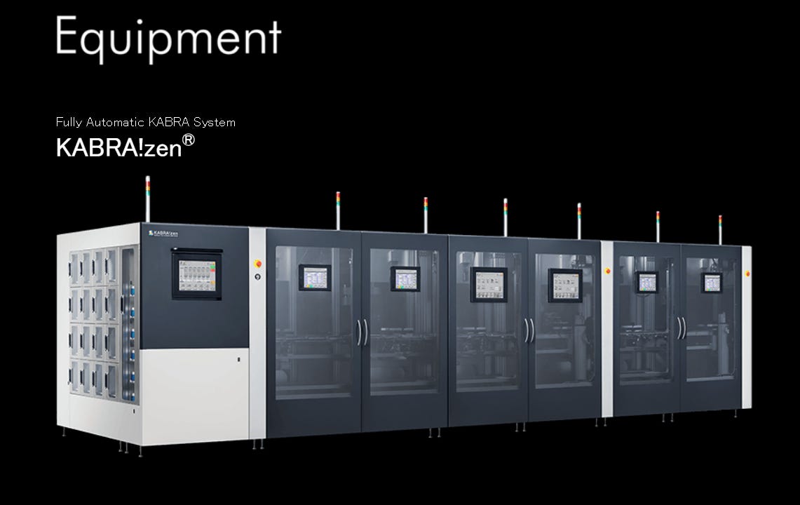
SiC is used in power semiconductors and can withstand high temperatures and high voltages, making it a key material for electric vehicles and renewable-energy systems.
DISCO’s grinding and polishing technologies can process thin chips and reduce surface damage, supporting substrates for HBM memory used in AI servers as well as automotive power modules.
Automotive, Power, and Specialty Semiconductors: Japan’s Vehicle-Centric Strength
Autonomous vehicles, electric vehicles, and automotive electronics rely heavily on specialized semiconductors. Japan holds a strong position in automotive MCUs, power devices, and analog components. This section discusses the strategies of Renesas Electronics and ROHM in AI and automotive applications.
Renesas: From an MCU Company to a Complete Embedded Computing Platform
Renesas is a global leading supplier of microcontrollers, or MCUs. It also provides SoCs, analog devices, and power components, holding important market positions in automotive, industrial, home appliance, and IoT markets.
Renesas offers complete hardware and software solutions covering sensing, connectivity, computing, and actuation, making it one of the world’s most influential MCU suppliers.
Renesas’ traditional strengths include:
Automotive MCUs;
Industrial MCUs;
SoCs;
Analog;
Power management
Connectivity;
Timing.
In 2025, Renesas’ automotive business remains an important pillar, while its industrial, infrastructure, and IoT businesses have grown on the back of stronger infrastructure demand. The company is also continuing to enhance its capabilities in vision AI and automotive AI software.
Renesas’ Role in AI Is Not Training Chips, but Edge AI
In AI, Renesas has launched a complete AI / ML developer stack supporting vision, voice, and real-time analytics. The company provides end-to-end support from sensing and connectivity to computing and actuation, along with a rich ecosystem of tools and partners.
To support this, Renesas provides various MCUs and RZ/A series processors, paired with eIQ software, enabling developers to implement ML inference on low-power microcontrollers.
Renesas’ AI role is mainly positioned in:
Smart vehicles;
ADAS
In-cabin AI;
Factory automation;
Robotics;
Smart sensing;
Edge vision;
IoT inference.
Unlike data center GPUs, Edge AI places greater emphasis on:
Low power consumption;
Real-time response;
Functional safety;
Long-term supply;
Cost;
Sensor integration;
Control loops;
Software tools.
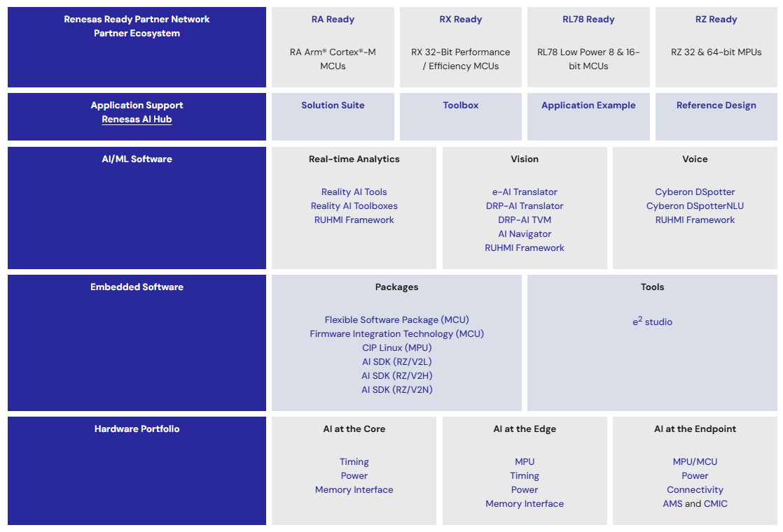
The Value of Automotive AI
Automotive AI is not only about autonomous driving.
It also includes:
• In-cabin driver monitoring;
• Voice recognition;
• Cockpit personalization;
• Radar and camera sensor fusion;
• Battery management;
• Predictive maintenance;
• Body control;
• Zonal architecture.
Renesas can extend upward from MCUs and control-side applications into SoCs and AI accelerators.
Renesas’ RH850/U2C automotive microcontroller is based on a 28 nm process and is primarily used in chassis and safety systems, battery management systems, lighting, and motor control.
It features a rich set of communication interfaces and low-power modes, while complying with ASIL D functional safety requirements and ISO / SAE 21434 cybersecurity requirements.
Renesas is described as a provider of advanced semiconductor solutions. Its MCU products combine embedded processing, analog, power, and connectivity technologies, making them suitable for automotive, industrial, and IoT markets.
AI and Future Direction
For future autonomous vehicles, Renesas is developing SoCs that support advanced driver-assistance systems such as L2+ and L3, while combining its analog and power devices to provide complete solutions.
Beyond hardware, Renesas has launched software frameworks such as eAI and Reality AI to support edge AI.
In the AI server market, Renesas participates through data converters and power ICs, but its core business remains focused on automotive and industrial markets.
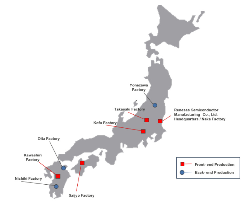
Front-end production site in Japan: 5 sites (Renesas Semiconductor Manufacturing Co., Ltd.)
Back-end production site in Japan: 3 sites (Renesas Electronics Corporation)
ROHM: Extending from EV SiC to AI Data Center Power Delivery
ROHM is a major Japanese manufacturer of analog and power semiconductors, and is particularly strong in SiC power devices.
According to the company’s official introduction, SiC devices offer lower conduction losses and smaller size compared with traditional silicon devices, enabling significant efficiency improvements. ROHM is one of the global pioneers in this field.
Through in-house SiC wafer production and packaging technologies, ROHM provides power solutions for electric vehicles, renewable energy, chargers, and industrial power systems.
ROHM’s core products include:
SiC MOSFETs;
SiC diodes;
GaN;
Silicon MOSFETs;
Power ICs;
Gate drivers;
Analog and power semiconductors.
In the past, the market mainly viewed ROHM as a beneficiary of EV SiC adoption. However, from 2025 to 2026, the company has clearly increased its visibility in AI data center power delivery.
ROHM has stated its support for the 800 V HVDC architecture promoted by NVIDIA and has released white papers related to 800 VDC power systems for AI data centers. In June 2026, ROHM also announced that its 750 V SiC MOSFET had been adopted for AI server BBUs.
Power and Analog Technologies
ROHM regards power semiconductors and analog technologies as its core strengths. By combining power modules with control ICs, the company provides comprehensive power solutions.
Its analog technologies are widely used in power management ICs, amplifiers, sensor interfaces, and other applications, supporting demand from IoT, AI, and autonomous driving.
ROHM integrates element development and module technologies to provide optimized power solutions.
Why do AI data centers need SiC?
As rack power moves from tens of kilowatts toward:
• 100 kW;
• 300 kW;
• 500 kW;
• 1 MW;
if power is still transmitted at low voltage, the current becomes extremely high.
The basic relationship is:
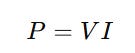
At the same power level, increasing voltage reduces current.
Conduction loss is:

Therefore, reducing current can significantly lower:
Copper loss;
Cable cross-sectional area;
Busbar size;
Heat generation;
Power distribution complexity.
This is the physical foundation of the 800 VDC architecture.
ROHM’s SiC can be applied in:
AC-DC conversion;
Solid-state transformers;
BBUs;
UPS systems;
800 VDC buses;
High-voltage DC-DC conversion;
Power shelves;
Data center energy storage.
ROHM has indicated that related 800 VDC and ±400 VDC systems are planned to begin mass production in the second to third quarter of 2026, with shipment volume expected to increase after 2027.
Fifth-Generation SiC MOSFETs
In 2026, ROHM announced its fifth-generation SiC MOSFETs, targeting applications including EVs, AI server power supplies, and industrial equipment.
Future competitive factors include:
Lower RDS(on);
Lower switching loss;
Lower gate charge;
Higher short-circuit withstand capability
Lower parasitic-inductance packaging;
Higher power density;
Module reliability;
Cost reduction for 8-inch SiC wafers.
Market Applications
In its 2026 PCIM exhibition press release, ROHM stated that it would showcase solutions for automotive electrification, covering traction inverters, onboard chargers, battery disconnection systems, EV thermal management, and embedded technologies.
In addition, ROHM also showcased high-efficiency power technologies for industrial applications, including SiC- and GaN-based solutions for renewable-energy systems, AI servers, data centers, and industrial power supplies.
This shows that ROHM is not only focused on automotive applications, but is also extending its power technologies into HPC and data center demand.
Future Development
As the world moves toward net-zero emissions, power devices such as SiC and GaN will be widely adopted in electric vehicles, charging stations, and energy storage systems.
ROHM continues to expand SiC wafer capacity and develop double-sided cooling packages.
For AI servers, power efficiency and high-current delivery are critical. ROHM’s SiC power modules can help reduce energy consumption and increase output power density.
The company is also investing in AI server power supply design and integration, emphasizing coordination between power delivery and control ICs.
Advanced Packaging and the 3D Fabric Ecosystem: Enabling the Scaling of AI Accelerators
AI models and HPC servers require higher-density integration of more chips and memory, driving the development of 2.5D / 3D packaging, chiplet designs, and high-bandwidth memory. Japan holds key positions in the global supply chain for package substrates, passive components, materials, and precision processing.
This section introduces the roles of IBIDEN, Shinko Electric, Kyocera, Murata Manufacturing, Resonac, TDK, and Taiyo Yuden in the advanced packaging ecosystem.
IBIDEN: A Core Supplier of ABF Substrates Behind High-End AI Processors
IBIDEN’s electronics business is centered on high-end IC package substrates.
IBIDEN mainly provides IC package substrates and printed circuit boards, while also possessing technologies in areas such as diesel particulate filters, or DPFs, and specialty carbon products. As demand for AI and HPC servers surges, the company has decided to make significant investments in capacity expansion.
High-end ABF substrates are used in:
CPUs;
GPUs;
AI ASICs;
Network switch chips;
HPC chips.
AI Server Investment Plan
In 2026, IBIDEN announced that its board of directors had resolved to invest approximately ¥500 billion from 2026 to 2028 to build new capacity at its Ogaki and Onomichi plants in Gifu Prefecture. The investment is intended to expand production capacity for high-performance IC package substrates in order to meet demand from AI servers and high-performance servers.
The plan is expected to begin operations in fiscal 2027, with the goal of supplying strong demand after 2027.
The press release also emphasized IBIDEN’s main businesses: its electronics business focuses on plastic packages, printed circuit boards, and related products, while its ceramics business focuses on diesel particulate filters and specialty carbon products, collaborating with global companies on technological innovation.
This investment shows IBIDEN’s commitment to supplying the large-size, high-layer-count package substrates required for AI servers, as AI accelerators require higher I/O counts and larger circuit areas.
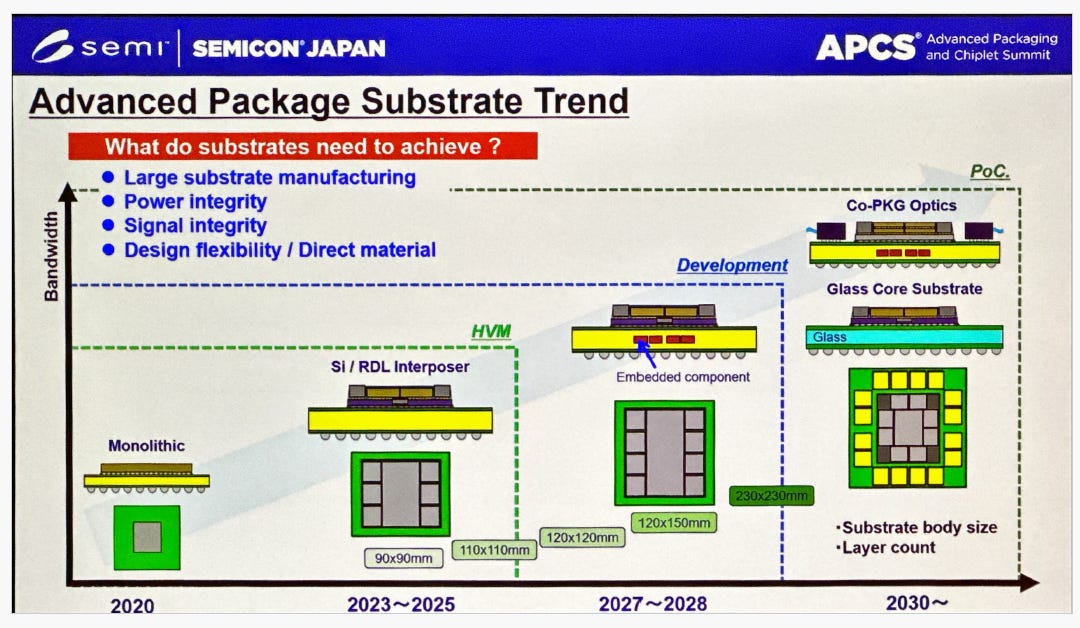
Why do AI GPUs need more advanced substrates?
As AI chip package sizes continue to increase, substrates must handle:
More power and ground connections;
More high-speed signals;
Larger package bodies;
Higher current;
Lower impedance;
Finer line width and spacing;
Higher layer counts;
Lower warpage.
An ABF substrate is not merely a carrier for chips. It connects:
Silicon interposers;
GPUs;
HBM;
PCBs;
VRMs;
External high-speed I/O.
Future Outlook
As AI models continue to scale rapidly, the layer count and size of package substrates will continue to increase.
IBIDEN’s capacity expansion is expected to strengthen its position in the high-end substrate market and support collaboration with global CPU and GPU vendors in the adoption of 2.5D interposers.
The company may also enter the field of organic interposers to address the future trend toward panel-level packaging.
Risks
Large-scale capacity expansion requires substantial capital investment;
Customer concentration risk;
Competition from Unimicron, Nan Ya PCB, Kinsus, and other Asian suppliers beyond IBIDEN;
If substrate-less architectures such as CoWoP mature, they may change long-term demand for traditional ABF substrates.
However, it is important to note that CoWoP does not mean all substrate demand will disappear immediately. In the short to medium term, large AI packages will still require high-end substrates. Even if some architectures connect directly to PCBs, demand for more advanced mSAP, HDI, and localized interposer-like structures is still likely to increase.

Shinko Electric: An Integrated Supplier of Packaging Technologies and Substrates
Shinko Electric is an important player in IC packaging and substrates, providing a broad range of packaging technologies from single-chip packaging to module assembly.
The company is committed to developing new interconnect technologies to support packaging requirements for high-end chips.
Its core technologies include hermetic sealing, ceramic processing, multilayer formation, IC assembly, photolithography / etching, plating, and mold fabrication.
Shinko’s product lineup includes:
•Device Embedded Package, or MEP: embeds chips inside printed circuit boards, reducing package thickness and shortening electrical paths.
•Flip-chip packages, or FC packages: including molded underfill and lids, used for high-power chips such as CPUs and GPUs.
•Power device packages: packaging solutions for power semiconductors.
•Optical chiplet assembly and co-packaged optics, or CPO: co-packaging optical chips and electronic chips for high-end servers and communication equipment.
Shinko’s optical chiplet and CPO page explains that optical chip packaging provides efficient optical interconnection between photonic integrated circuits, or PICs, and electronic integrated circuits, or EICs. CPO integrates optical communication into xPU packages, including CPUs, GPUs, and other processors.
Applications include high-end servers and networking equipment, providing solutions for 800G and higher-speed optical modules.
Compared with IBIDEN, Shinko’s key characteristic is that it extends beyond substrates into a broader range of packaging-related products.
Its AI opportunities come from:
HPC substrates;
High-end CPUs and GPUs;
HBM packaging;
Thermal structures;
Advanced packaging assembly.
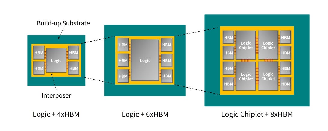
Future Value
Competition in AI packaging will not be determined by a single substrate alone. Instead, it will be shaped by the combined performance of:
Substrates;
Heat spreaders;
TIMs;
Stiffeners;
Underfill;
Lids;
Assembly.
Together, these factors determine yield and thermo-mechanical reliability.
If Shinko can integrate substrates, packaging, and thermal solutions, it can increase its system-level value within the AI packaging supply chain.

Market Position and Core Technologies
Shinko’s business page states that IoT, AI, and autonomous driving will make semiconductor applications more widespread. The company aims to cover the entire semiconductor packaging field, with products applied in devices, servers, home appliances, industrial machinery, automobiles, and other markets.
The company possesses core technologies including hermetic sealing, ceramic processing, multilayer formation, IC assembly, photolithography, and etching.
Looking ahead, Shinko will continue to develop new substrates and optical-electrical hybrid packaging, while collaborating with customers on the design of optical-electrical coupling devices to meet the needs of AI and high-speed communications.

Kyocera: From Traditional Ceramic Packaging to Core Substrates and High-Speed Optical Modules for AI
Kyocera is known for its fine ceramic technologies and holds an important position in electronic components, ceramic packages, and related modules. In recent years, as AI servers have driven demand for high-density chip packaging, Kyocera has also provided related solutions.
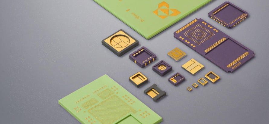
Kyocera’s semiconductor-related capabilities include:
Ceramic packages;
AlN substrates;
HTCC / LTCC;
High-reliability packaging;
Optical communication components;
Crystal devices;
High-frequency components.
In April 2026, Kyocera announced the commercialization of multilayer ceramic core substrates, targeting applications such as xPUs and switch ASICs for AI data centers.
This move is highly significant because it shows that Kyocera is moving from traditional high-reliability ceramic packaging into the market for large-scale AI semiconductor substrates.
New Ceramic Core Substrates
In April 2026, Kyocera announced that it had commercialized multilayer ceramic core substrates for advanced semiconductor packages used in xPUs and switch ASICs.
The substrate uses Kyocera’s proprietary high-rigidity fine ceramic material, which can reduce deformation in large packages and support high-density 3D routing.
The press release noted that the development of generative AI and large language models is driving demand for higher-performance xPUs and ASICs. These devices require larger and denser package substrates. Kyocera’s new substrate provides high rigidity, three-dimensional wiring, and customized design support, making it an essential material for 2.5D packaging.
Kyocera also provides thermal, electrical, and substrate-warpage simulation services, helping customers address potential issues from the design stage.
Ceramic materials may offer:
Higher modulus;
Higher dimensional stability;
Good heat resistance;
Adjustable CTE;
High insulation performance;
Good thermal conductivity;
Suitability for high-frequency and high-reliability applications.
Among these materials, AlN provides relatively high thermal conductivity, making it suitable for power devices and high-heat-flux applications.

Comparison with Glass Cores

If Kyocera’s multilayer ceramic core can solve challenges such as:
Large-area co-firing;
Interlayer alignment;
Via metallization;
Flatness;
Cost;
it could become a differentiated solution for AI ASICs, switch ASICs, optical-electrical packaging, or high-reliability HPC applications.
Characteristics of Ceramic Packaging
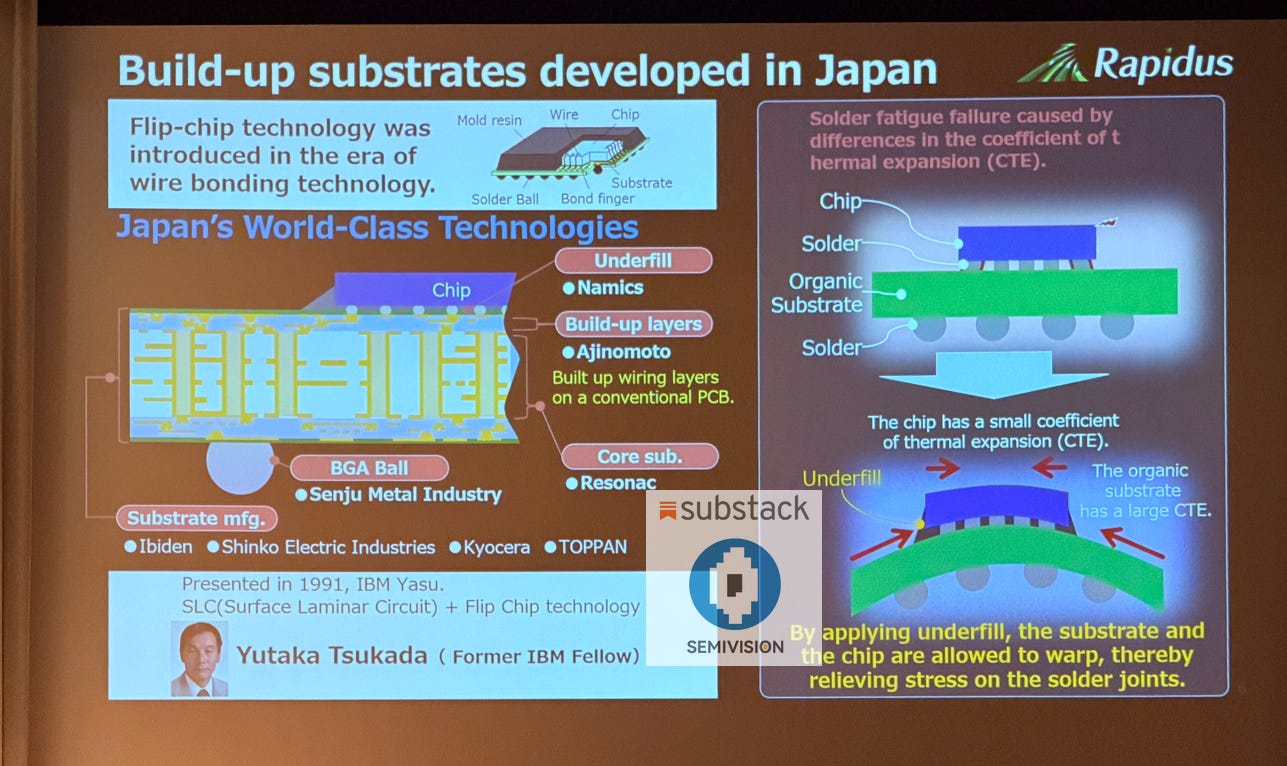
In its explanation of ceramic packaging, Kyocera states that ceramic packages are widely used in products requiring high reliability because of their high strength, high thermal conductivity, and design flexibility.
Ceramic packaging can support 3D packaging and miniaturization. A wide range of ceramic materials is available, and their thermal expansion coefficients can be well matched with semiconductor materials to ensure reliability.
Therefore, for the high power density and thermal requirements of AI servers, ceramic substrates can reduce warpage and provide excellent thermal management.
Optics and AI Data Centers
Kyocera also announced in 2026 a pluggable optical-electrical module supporting PCIe 6.0, showing that its strategy is not limited to passive packaging but is also extending into high-speed interconnects for AI data centers.
Future Outlook
Kyocera will further develop high-density ceramic substrates and integrate metallized wiring to support xPUs with trillions of transistors.
For 3D IC and chiplet designs, ceramic packaging may be used alongside organic substrates and silicon interposers to balance performance and cost.
The company may also expand ceramic thermal modules and modular power solutions to support AI servers and automotive electronics.

2025年10月27日
Murata Manufacturing
Murata Manufacturing is a global leader in passive components. Its products include multilayer ceramic capacitors, or MLCCs, inductors, filters, wireless modules, and power modules. The company holds important positions in fields such as AI, automotive electronics, and communication devices.

Passive Component Innovation and AI
Five of them, with rated voltages of 2.5 V to 4 V, are used in peripheral IC circuits for advanced driver assistance systems, or ADAS, and autonomous driving, or AD. The other two, with rated voltages of 25 V, are used in in-vehicle power lines.
Because ADAS and AD systems require stable power supply and miniaturized components, Murata has achieved high capacitance in compact sizes through materials technology and particle miniaturization. This helps reduce PCB area while stabilizing power delivery.
Another press release introduced Murata’s participation in Sensors Converge 2026. Murata is a global leader in the design, manufacturing, and sales of ceramic-based passive components, communication modules, and power modules. The company is committed to developing advanced electronic materials and high-density modules, and operates production and sales sites worldwide.
Murata also emphasizes innovation in sensing and connectivity technologies, supporting AI-driven smart mobility, healthcare, and industrial applications.
Role in AI Servers
AI servers require large quantities of high-capacitance MLCCs and inductors to handle high current and reduce noise.
As one of the largest MLCC suppliers, Murata’s products are widely used in server motherboards, GPU modules, and power modules.
At the same time, Murata is also developing power modules and wireless modules to support interconnectivity in AI servers and cloud infrastructure.
Looking ahead, Murata will continue to pursue higher capacitance density, smaller form factors, and high-reliability, high-temperature specifications to meet the needs of data centers and automotive electronics.
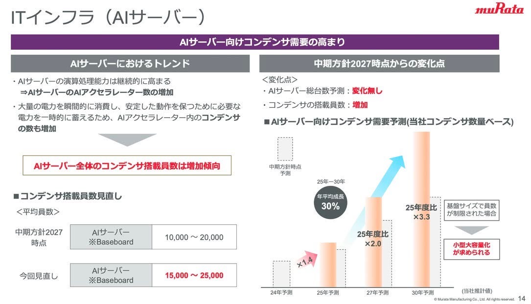
Murata highlights the rising capacitor demand in AI servers. As AI server computing performance continues to increase, the number of AI accelerators per server is also growing. To maintain stable operation under large and rapidly changing power loads, each accelerator requires more capacitors to temporarily store and deliver power. As a result, the total capacitor count per AI server is trending upward.
Murata has revised its estimate for capacitor usage on AI server baseboards. Its previous medium-term 2027 assumption was around 10,000–20,000 capacitors per baseboard, but the latest revision raises this to approximately 15,000–25,000 units.
The company also expects AI server unit shipments to remain largely unchanged, while capacitor count per server will increase. Based on Murata’s capacitor-volume forecast, AI server capacitor demand could grow at an average annual rate of around 30%, reaching 2.0 times 2025 levels by 2027 and 3.3 times by 2030.

6月15日
Resonac
Resonac was formed through the merger of Showa Denko and Hitachi Chemical. The company mainly provides semiconductor materials, including encapsulation materials and adhesives, as well as functional materials and chemicals.
Resonac emphasizes the use of materials innovation to enable advanced packaging and 3D packaging.
Panel-Level Packaging and the JOINT3 Alliance
In September 2025, Resonac announced the establishment of the JOINT3 alliance with 26 companies, targeting the development of next-generation semiconductor packaging technologies, particularly panel-level organic interposers.

Advanced packaging is critical for next-generation semiconductors. As data transmission volume and speed continue to increase, demand is shifting toward 2.xD packaging, where multiple chips are placed on an interposer.
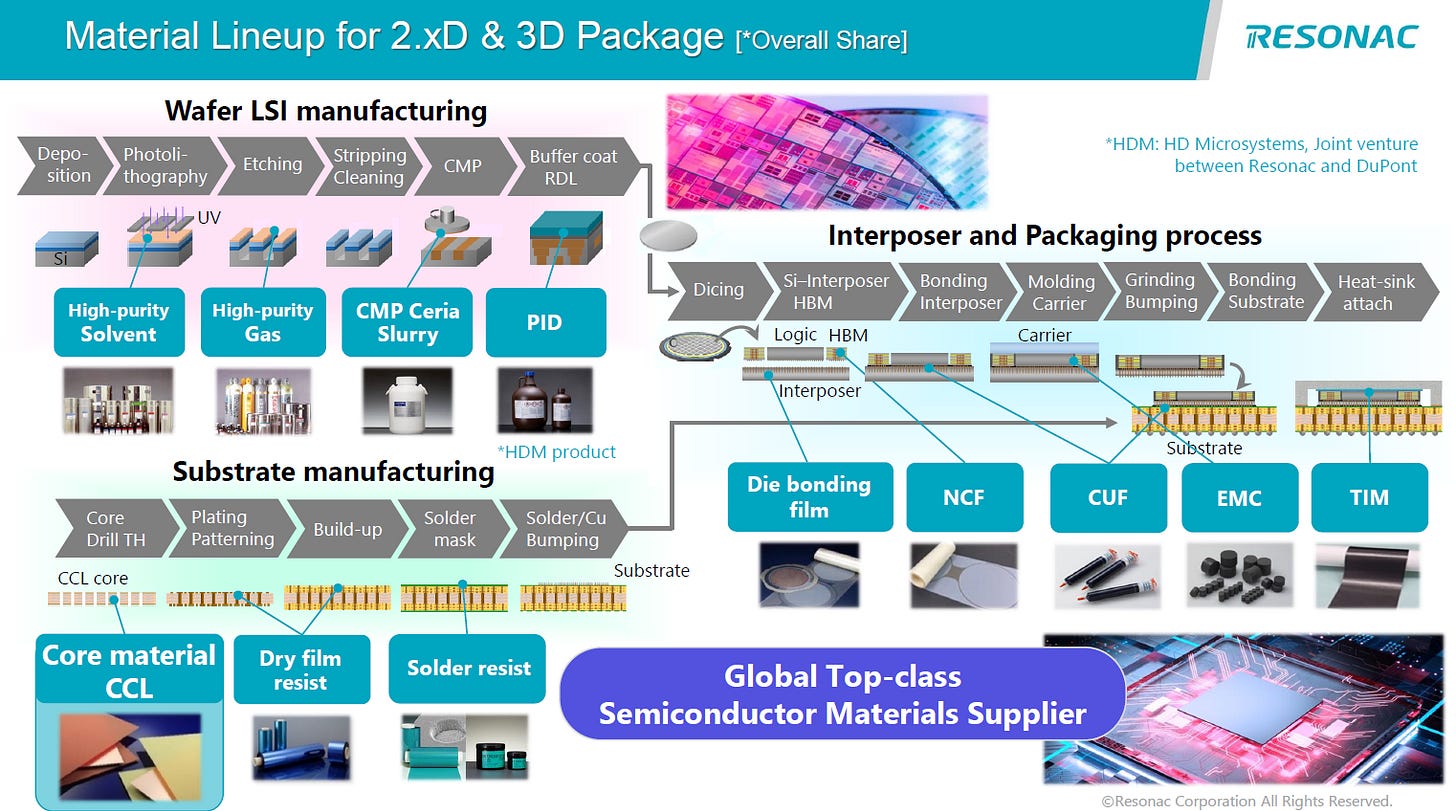
As a result, interposer sizes are becoming larger. The industry is shifting from silicon interposers to organic interposers, and from circular wafer-based manufacturing to square panel-based manufacturing, in order to improve production efficiency.
Resonac will establish the Advanced Panel-Level Interposer Center, or APLIC, at its Shimodate Plant. The facility is scheduled to begin operations in 2026 and will include a prototype production line.
Members such as Tokyo Electron have stated that advanced packaging requires miniaturization, high-speed signal transmission, and scaling. Through alliance-based collaboration, AI semiconductor technology can be advanced significantly.

2025年2月13日
Semiconductor Back-End Materials
Resonac’s product pages state that the company provides a wide range of semiconductor back-end process materials and holds large market shares globally.
Through its Packaging Solution Center and JOINT2, Resonac is jointly developing advanced technologies such as 3D packaging and working to accelerate the launch of next-generation packaging solutions.
Product categories include pre-applied packaging films, or FAL-F, magnetic molding compounds, dicing tapes, release films, and QFN map molding support tapes.
These materials are used for package sealing, inductor molding, chip dicing, and molded packaging, supporting the manufacturing of AI accelerators and complex modules.
Future Development
Resonac is actively developing panel-level packaging materials and engineering services to address the needs of chiplets and large interposers.
Through the JOINT3 alliance and the APLIC facility, the company aims to improve the performance of organic interposers and packaging materials, supporting large-scale AI accelerators and HPC demand.
Resonac is also promoting products such as low-temperature adhesive materials, thermal interface materials, and RF packaging materials to meet diverse application requirements.

2024年11月11日
TDK
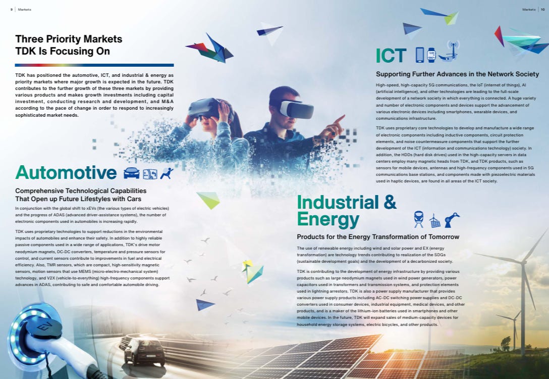
TDK is a global leader in electronic components and materials. Its products cover magnetic materials, passive components such as capacitors and inductors, sensors, energy devices, and more.
TDK emphasizes providing comprehensive solutions from edge devices to servers in an AI-driven society.
AI Ecosystem Strategy
A indusry report titled “How Electronic Components Support an AI-Driven Society” stated that TDK is committed to developing high-efficiency passive components and power products to reduce energy consumption in AI servers and data centers. Its goal is to reduce power loss while supporting massive data processing requirements.
TDK provides complete AI ecosystem solutions, including edge AI modules, or edge RX, ultra-compact full-color laser modules for AR glasses, as well as various sensors, batteries, and software.
For AI servers and optical transceivers, TDK pointed out that servers require stable power supply and noise suppression. The company uses VLBUC and ERUC series inductors, along with multilayer ceramic capacitors, or MLCCs, to provide voltage regulation and noise reduction. A single AI server may contain thousands of MLCCs and inductors.
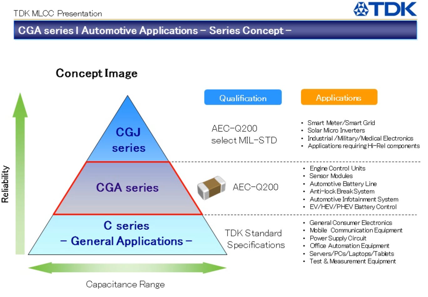
To improve performance, TDK is also developing compact power inductors and thin-film capacitors for optical transceivers.
The company also applies factory automation technologies to develop load ports and flip-chip bonding systems for semiconductor manufacturing equipment, supporting the broader AI ecosystem.
In addition, TDK integrates technologies such as sensors, imaging devices, batteries, and software to create innovation platforms for autonomous vehicles, smart homes, and healthcare. The company will continue improving electronic components to support an AI-driven society.
Future Outlook
As AI applications become more widespread, TDK will invest more resources in developing low-loss, high-frequency passive components, energy harvesting devices, and embedded modules.
The company will also expand collaboration in sensors and energy technologies, while using AI algorithms to improve component performance.
For wafer fabrication equipment, TDK can use its factory automation capabilities to provide chip handling and bonding equipment, further expanding its vertical integration.
Taiyo Yuden
Taiyo Yuden is a world-class passive component manufacturer and is known for producing some of the smallest MLCCs in the world. Its products are used in communication devices, data centers, automotive electronics, and other applications.
Its homepage states that the company is a global electronic component manufacturer that produces the world’s smallest MLCCs and contributes to electrification across various applications, including communication devices, through cutting-edge passive components such as capacitors and inductors.
Ultra-High-Capacitance MLCCs for AI Servers
A PR Newswire release in October 2025 stated that Taiyo Yuden had begun mass production of an embedded MLCC measuring 1.0 × 0.5 mm, or 1005M size, with a capacitance of 22 µF. The product is used for IC power decoupling in AI servers.
Because ICs in AI servers consume enormous amounts of power, compact, high-capacitance MLCCs must be placed close to the IC to reduce circuit loss and noise.
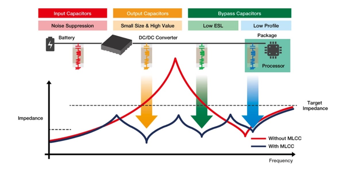
High-reliability and a reduced size can be achieved by utilizing multilayer ceramic capacitors with a lower ESR and ESL than electrolytic capacitors in power supply circuits.
To achieve this, Taiyo Yuden improved its external electrode formation technology and began mass production at its Tamamura Plant, while continuing to develop even higher-capacitance MLCCs.
The press release noted that embedded MLCCs can be placed close to ICs, reducing inductance and noise while providing a more stable power supply. They are indispensable components for AI servers.

Future Outlook
Taiyo Yuden will continue to develop MLCCs and inductors with higher capacitance and higher voltage ratings to support high-frequency applications such as AI and 5G.

The company is also expected to develop embedded passive device, or EPD, technologies, embedding passive components into substrates to provide shorter signal paths and better electrical performance.
For automotive electronics, Taiyo Yuden also provides high-temperature-resistant capacitors and sensors to meet the needs of electric vehicles.
Conclusion and Future Trends
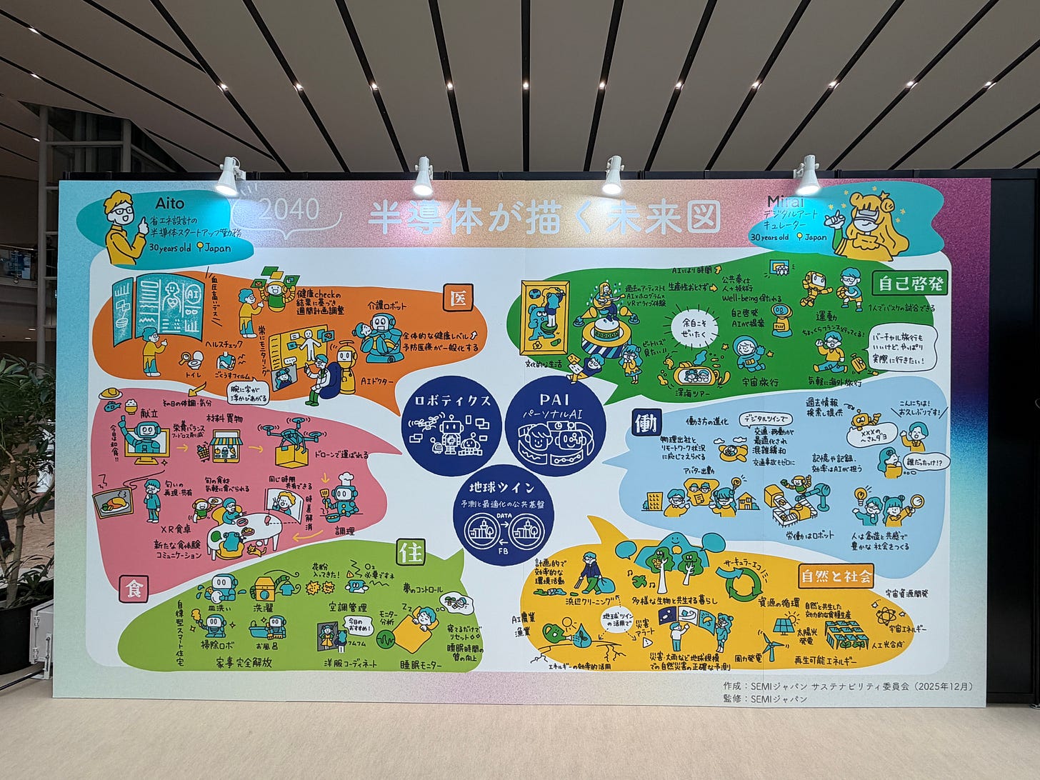
Strengths and Challenges of Japan’s Semiconductor Industry
Looking across the companies discussed above, Japan holds several key strengths within the semiconductor supply chain:
•Leadership in manufacturing equipment and materials: Companies such as Tokyo Electron, SCREEN, Kokusai Electric, Lasertec, Advantest, and Tokyo Seimitsu possess world-leading technologies in etching, deposition, cleaning, testing, and inspection. These tools are indispensable for advanced semiconductor manufacturing and support global fabs, especially in sub-3 nm process nodes and 3D packaging. Materials suppliers such as SUMCO and Resonac control core supplies of silicon wafers and packaging materials.
•Passive components and power semiconductors: Murata, Taiyo Yuden, TDK, and ROHM provide high-quality passive components and power devices that support AI servers, automotive electronics, and communication equipment. ROHM, a leader in SiC technology, provides high-efficiency power modules for electric vehicles, while passive component suppliers support global PCB and module demand and are difficult to replace.
•Package substrates and advanced packaging technologies: IBIDEN, Shinko Electric, and Kyocera have strong capabilities in substrates and packaging, while Resonac provides key materials, forming a comprehensive 3D packaging ecosystem. The establishment of the JOINT3 panel-level packaging alliance shows that Japan is collaborating with global companies to develop next-generation large-size interposers.
•Strength in automotive electronics and MCUs: Renesas and ROHM have captured strong positions in automotive and industrial markets, providing functional safety and power module solutions while benefiting from the growth of electric vehicles and autonomous driving.
However, Japan’s semiconductor industry also faces several challenges:
•Lagging advanced logic manufacturing: Compared with South Korea, Taiwan, and the United States, Japan lacks a domestic leading-edge logic foundry. Although Rapidus was established with the goal of mass-producing 2 nm process technology, it still requires substantial investment and international collaboration.
•Intensifying global competition: China, South Korea, Taiwan, and the United States are investing heavily to expand wafer fabrication capacity. Japanese companies must maintain competitiveness through collaboration, acquisitions, and technology differentiation.
•Talent and cost pressure: Japan’s declining birthrate and high-cost environment may affect investment. Continued government subsidies and industrial policy support will be necessary.
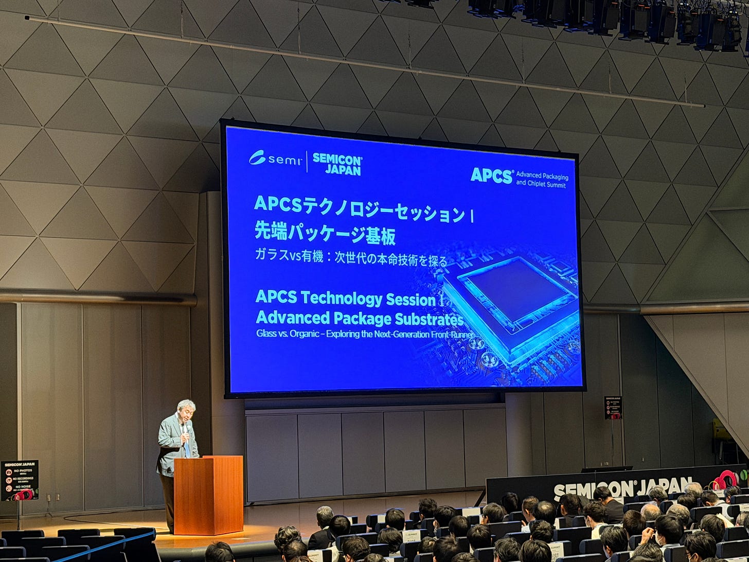
AI and Future Technology Outlook
AI, machine learning, IoT, and edge computing will continue to drive semiconductor demand. The following are key future trends:
2.5D / 3D Packaging and Chiplets
To improve computing power and reduce power consumption, chips will increasingly adopt chiplet architectures and use 2.5D or 3D packaging.
IBIDEN, Shinko Electric, and Kyocera are expanding capacity for high-end package substrates and ceramic core substrates, while Resonac is investing in panel-level interposers. These technologies are expected to support large-scale AI accelerators.
High-Bandwidth Memory and HBM
AI models require enormous memory bandwidth, driving an increase in the number of HBM stack layers. This will also increase demand for testing and dicing.
Advantest’s AI-driven test platforms and DISCO’s low-damage dicing technologies will become increasingly important.
Power Efficiency and Thermal Management
AI servers consume large amounts of power, making power efficiency and thermal management key system bottlenecks.
ROHM’s SiC modules, Renesas’ power management ICs, and passive components from TDK, Murata, and Taiyo Yuden collectively improve energy efficiency.
Kyocera’s ceramic substrates and Resonac’s packaging materials also provide better thermal management.
AI-Driven Process and Yield Management
Manufacturing equipment will increasingly adopt AI and machine learning for predictive maintenance, process optimization, and defect detection.
Examples include TEL’s digital twins, Advantest’s AI-driven testing, and Lasertec’s AI-based inspection analytics.
These technologies can reduce production costs and accelerate mass-production ramp-up.
Automotive and Edge AI
As autonomous driving and smart cities continue to develop, demand for automotive MCUs and power devices will remain strong.
Renesas and ROHM will expand their product lines toward L3 and L4 driving applications and collaborate with AI algorithm developers to optimize systems.
Edge AI requires low-power, miniaturized processors and passive components. Murata and Taiyo Yuden will provide high-reliability MLCCs, while TDK will support AR and IoT applications through edge RX modules.
Materials Innovation and Sustainability
To achieve carbon neutrality, semiconductor manufacturing processes must reduce energy and chemical usage.
For example, SCREEN’s SU 3200 and SU 3300 cleaning systems reduce consumables through optimized control. TEL and Resonac are also exploring recyclable materials and lower-energy processes.
In the future, solvent-free adhesives, low-temperature solders, and renewable materials will receive greater attention.

2025年7月19日
Final Remarks
Although Japan’s semiconductor companies are relatively weaker in leading-edge logic wafer fabrication compared with other regions, they possess irreplaceable strengths in equipment, materials, testing, packaging, and power devices.
This report has examined more than a dozen companies from the perspectives of technology, products, market positioning, and their roles in AI, outlining a panoramic view of Japan’s semiconductor industry.
As global demand for AI and high-performance computing continues to rise, the technological innovation and capacity investments of these companies will shape the future competitive landscape.
Through government policy, industry-academia collaboration, and international alliances, Japan is well positioned to maintain a critical role in the AI era and make significant contributions to the global semiconductor ecosystem.

6月11日


PreviousNext