Huawei’s “Tao Law”: τ Explains the Direction, Hi-ONE Faces the Physics
Huawei’s “Tao Law”: τ Explains the Direction, Hi-ONE Faces the Physics
- Source: SemiVision
- Author: SEMIVISION
- Published: 2026-05-30T11:40:57+08:00
- URL: https://tspasemiconductor.substack.com/p/huaweis-tao-law-explains-the-direction (1) Huawei’s “Tao Law”: τ Explains the Direction, Hi-ONE Faces the Physics


Huawei’s “Tao Law”: τ Explains the Direction, Hi-ONE Faces the Physics
Original Article By SemiVision Research [Reading time: 15 mins]

May 30, 2026
∙ Paid
Huawei’s “Tao Law”: τ Explains the Direction, Hi-ONE Faces the Physics
Huawei’s recent introduction of “Tao Law” naturally draws attention to the phrase “new law.” But from an engineering perspective, the most important part is not the symbol τ itself. What matters is how Huawei is using this symbol to reorganize several post-Moore technology directions into one unified narrative.

The semiconductor industry has always been optimizing time.
The critical path is time. RC delay is time. Memory latency is time. SerDes latency is also time. Over the past several decades, the industry has compressed different layers of time constants by shrinking transistors, increasing frequency, shortening signal paths, improving interconnect materials, and advancing packaging structures.
So the statement that “the next frontier is no longer only scaling transistor dimensions, but scaling system time constants” is not a completely new physical discovery. It is more like a new language framework that reorganizes several things already happening across the post-Moore landscape.
But that does not mean it has no value.
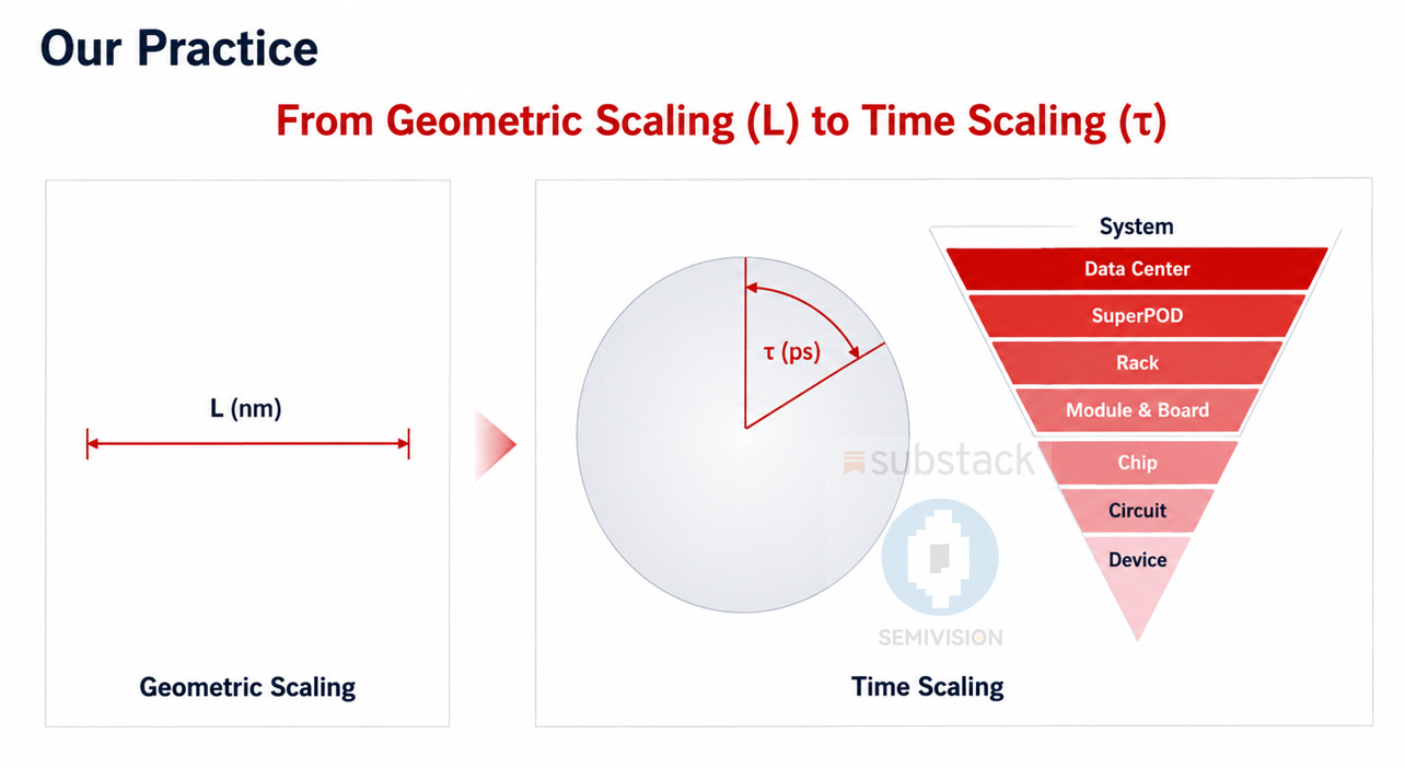
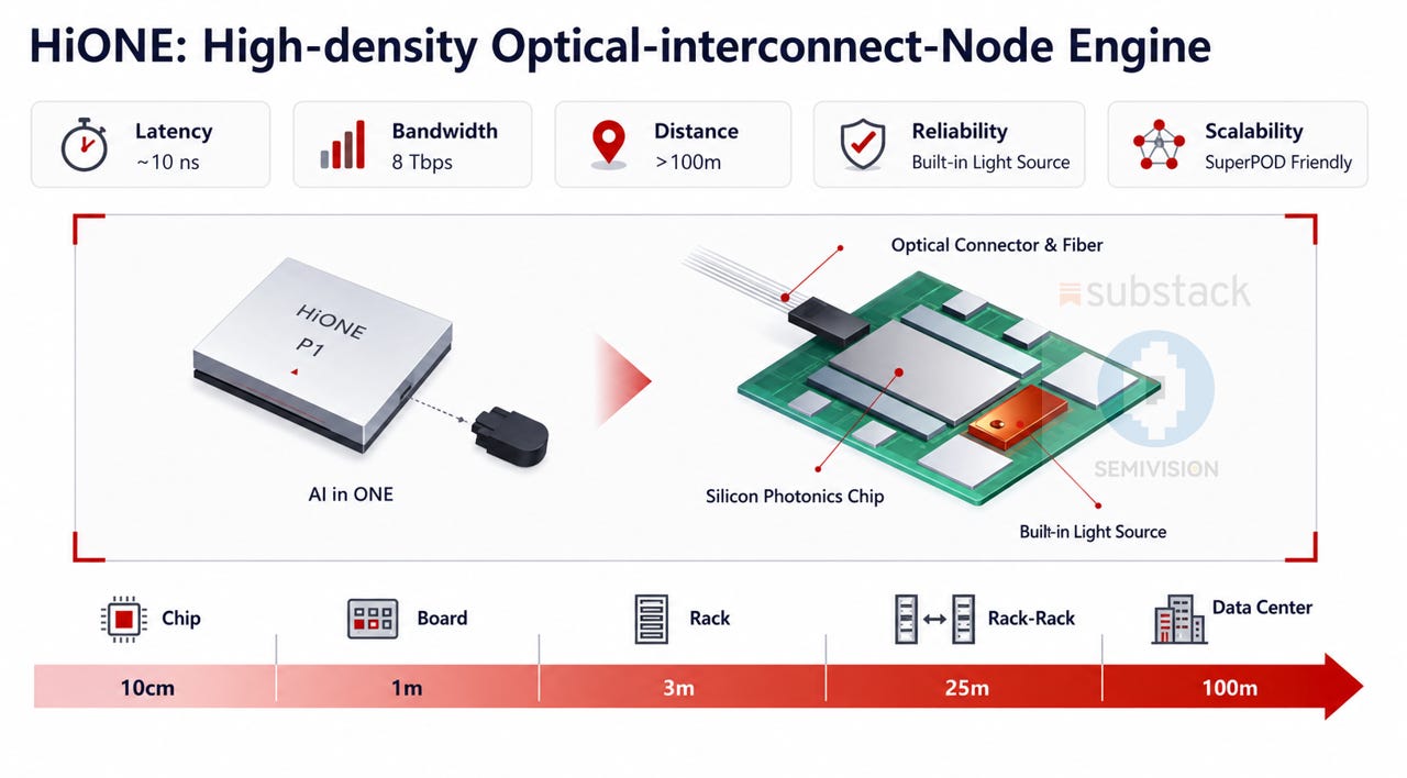
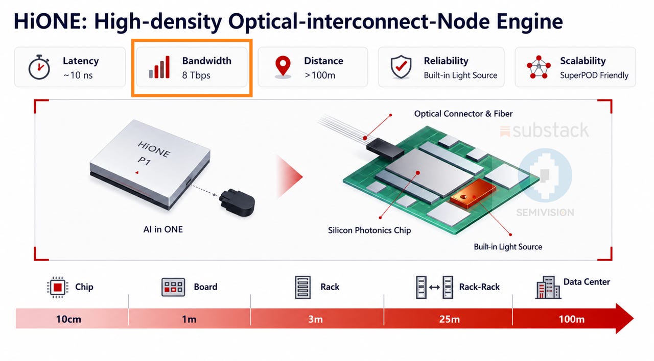
What makes Huawei’s proposal interesting is that it does not stop at the slogan level. In Huawei’s 2026 ISSCC presentation, the narrative moves from geometric scaling to time scaling, and then extends across device, circuit, chip, module, rack, SuperPOD, and data center levels. In the HiONE section, Huawei explicitly lists around 10ns latency, 8Tbps bandwidth, more than 100m distance, built-in light source, and SuperPOD-friendly characteristics. This means Hi-ONE is not an isolated optical module. It is a physical-layer answer to Huawei’s attempt to make an AI system behave more like one large machine.

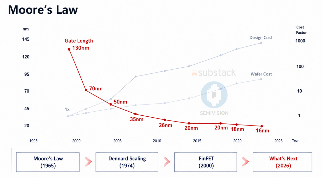
What is Moore’s Law?
Below we will share:
τ Is a Shared Language for the Post-Moore Era, Not a Huawei-Exclusive Physical Law
From Logic Folding to System Folding: Huawei Wants to Fold the System
The First Question for Hi-ONE: Is It CPO or NPO?
The Second Question: Why Put the Light Source Inside?
The Third Question: 8Tbps Is Not the Answer. pJ/bit Is the Answer
Hi-ONE’s Position in the Global Optical Interconnect Spectrum
τ Is a Shared Language for the Post-Moore Era, Not a Huawei-Exclusive Physical Law
Huawei defines “Tao Law” as a shift from geometric scaling to time scaling. At the industry-logic level, this direction is valid.
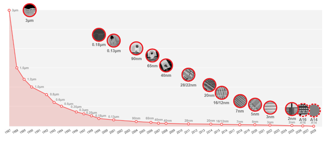
The core of traditional Moore’s Law was the coordinated scaling of transistor density, gate length, die cost, and performance per watt. But after advanced nodes entered 5nm, 3nm, and 2nm, the marginal benefit of geometric scaling has clearly declined. EUV cost, design cost, yield ramp, interconnect RC delay, the memory wall, power delivery, and thermal density have all become system-level bottlenecks.
5月14日
Therefore, post-Moore performance improvement is no longer just about making transistors smaller. More importantly, it is about:
Bringing data closer
Bringing memory closer to compute
Shortening the distance that electrical signals travel through copper
Reducing interconnect pitch inside packages
Lowering protocol-layer overhead
Treating multiple chips, racks, and nodes as one jointly optimized system.
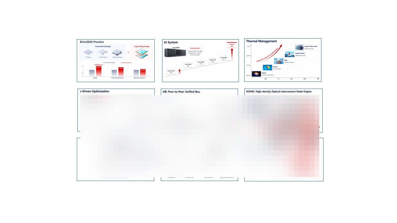
This is why Huawei’s presentation discusses logic folding, hybrid bonding, TSV, HBM, UnifiedBus, HiONE, SuperPOD, and thermal management at the same time. In AI infrastructure, the bottleneck is no longer a single transistor. It is the time, energy, and reliability cost of moving data across the entire system.
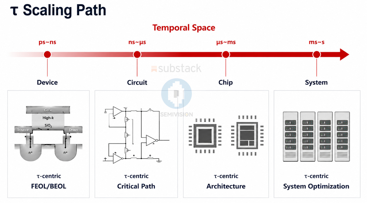
In other words, τ itself is not the answer. τ is a summarizing language.
It connects engineering problems originally scattered across device, circuit, chip, package, board, rack, and data center levels through the idea of “time constants.”
From Logic Folding to System Folding: Huawei Wants to Fold the System
If we only look at the name “Tao Law,” it is easy to think Huawei is proposing a new industrial law similar to Moore’s Law. But based on the technical content, it is closer to a system-engineering methodology for the post-Moore era.

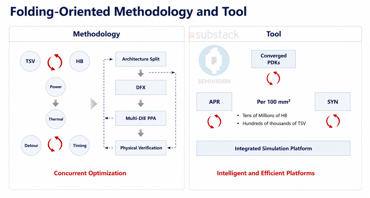
On the mobile application side, Huawei discusses Kirin logic folding. The core idea is that when planar 2D scaling becomes constrained, the critical path that was previously stretched horizontally can be folded vertically through 3D stacking, hybrid bonding, TSV, top metal, and vertical connection.

This is not magic. It is physics.
When physical distance is shortened, RC delay declines, the critical path becomes shorter, and both frequency and power efficiency can improve.
Huawei’s presentation also mentions folding-oriented device and process technologies, including hybrid bonding alignment, low-temperature bonding, TSV scaling, TSV yield, landing layers, and routing resources. These are all very concrete packaging and process problems. In other words, the difficulty of logic folding is not the concept. The difficulty lies in alignment precision, thermal budget, TSV yield, metal-layer redistribution, EDA flow, DFX, and multi-die physical verification.

At the AI system level, Huawei scales this logic into system folding.
Inside an AI SuperPOD, the number of chips may move from hundreds to thousands, while single-chip power consumption may move from the kilowatt level toward several kilowatts or even higher. At that point, the key question is no longer whether a single chip is fast enough. The real questions become:
How are chips connected?
How is memory brought closer to compute?
How is protocol overhead reduced across multiple nodes?
How is rack-to-rack latency reduced?
How is energy per bit reduced inside the data center?
When one node fails, how does the system maintain reliability?
This is the background behind Huawei’s UnifiedBus and Hi-ONE.
UnifiedBus answers the question of how the system communicates. Hi-ONE answers the question of how that communication actually runs in the physical world.

The First Question for Hi-ONE: Is It CPO or NPO?
Hi-ONE stands for High-density Optical interconnect-Node Engine.
According to Huawei’s presentation, HiONE offers 8Tbps bandwidth, around 10ns latency, more than 100m distance, and a built-in light source. The diagram also shows a silicon photonics chip, optical connector and fiber, and built-in light source. These details indicate that Hi-ONE is not a traditional pluggable optical module mounted on the front panel of a chassis. It is an optical engine positioned much closer to the AI compute node.
But whether it should be classified as CPO or NPO still requires careful interpretation based on more public information.
CPO, or co-packaged optics, places the optical engine and the switching ASIC or AI ASIC on the same package substrate. The advantage is extremely short distance, which can significantly reduce the length of high-speed electrical signaling through copper and therefore reduce SerDes power and channel loss. But the cost is also extremely high. The optical engine has to face the high thermal flux near the ASIC, field serviceability becomes difficult, and package yield plus single-point failure risks become much more severe.
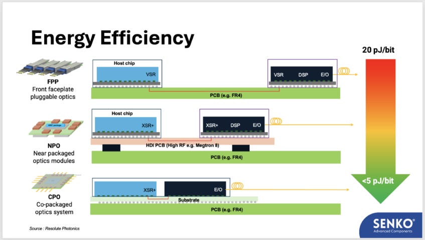
NPO, or near-packaged optics, places the optical engine around the ASIC at the board level, using very short electrical interconnects, fly-over cables, or high-density connectors to communicate with the ASIC. It is not as extreme as CPO, but the engineering difficulty is lower and serviceability is better.
Where Hi-ONE actually sits on this spectrum determines its true engineering envelope.
If it is closer to CPO, Huawei must answer a series of difficult questions around thermal coupling, package yield, field replaceability, laser lifetime, fiber attach, and optical alignment.
If it is closer to NPO, it may be easier to deploy, but the system will retain more SerDes power and latency than a true CPO implementation.
This is the first key issue to track for Hi-ONE.
The Second Question: Why Put the Light Source Inside?
Another very important detail is Hi-ONE’s built-in light source.
This is not the most conservative choice in the current global CPO and NPO technology landscape. Many mainstream optical I/O solutions for large-scale data centers and AI clusters tend to favor external laser sources.
The reason is simple: the thermal environment near an AI ASIC is extremely harsh.
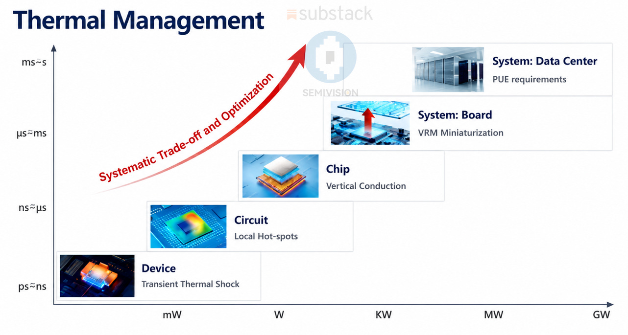
DFB lasers, EMLs, modulators, photodiodes, and TIAs are all sensitive to temperature, bias, aging, and optical power stability. The advantage of an external laser source is that the laser can be moved away from the high-temperature ASIC region, cooled separately, given separate redundancy, and maintained independently. When a laser degrades or fails, replacement is also easier.

But Hi-ONE uses a built-in light source. That means Huawei is choosing a harder path.
There are two possible explanations.
The first possibility is that Huawei has strong confidence in its optoelectronic packaging, thermal design, laser lifetime management, and system redundancy, and believes that an internal light source can deliver stronger advantages in system integration, latency, power, and modular deployment.
The second possibility is that supply-chain constraints prevent Huawei from fully relying on a standardized external laser source ecosystem, forcing the company to internalize more capabilities inside its own module.
The strategic meanings of these two possibilities are completely different.
The first is an active architectural choice. The second is an engineering reconstruction under supply-chain constraints.
Either way, the real test for Hi-ONE is not whether the demo can light up. The real test is whether, over a roughly eight-year data center lifecycle, it can maintain optical power, BER, thermal stability, serviceability, and large-scale deployment cost.
The Third Question: 8Tbps Is Not the Answer. pJ/bit Is the Answer
Hi-ONE’s 8Tbps bandwidth is an attractive headline number.
But for AI infrastructure, 8Tbps alone does not explain everything. Different lane configurations can produce the same aggregate bandwidth.
64 lanes of 128G can make 8Tbps.
40 lanes of 200G can make 8Tbps.
32 lanes of 250G can also make 8Tbps.
But these three architectures impose completely different requirements on optical modulators, drivers, TIAs, DSP, equalization, FEC, packaging density, test cost, and thermal design.
The real questions are not about aggregate bandwidth. The real questions are:
What is the per-lane data rate?
How many lanes are used?
Is DSP required?
Can pJ/bit be lower than traditional pluggable optical modules?
What is the effective bandwidth after FEC overhead?
What is the end-to-end latency?
How does BER behave under real workloads?
What are the optical engine yield and burn-in costs?
Can mass-production testing support such a high channel count?
After failure, do you replace the optical engine, replace the board, or scrap the entire core module?
AI cluster interconnect is not a laboratory benchmark game. It is a TCO game. When GPU, NPU, HBM, switch, NIC, optical engine, power module, and thermal system are all packed into a high-power, high-density, high-thermal-flux system, the final commercial result is not determined by one number. It is determined by the combined outcome of pJ/bit, availability, serviceability, yield, and deployment cost.
So if Hi-ONE wants to prove itself, it cannot only say “8Tbps.” It must show what price was paid to achieve that 8Tbps.
Hi-ONE’s Position in the Global Optical Interconnect Spectrum
From the perspective of the global optical interconnect landscape, Hi-ONE’s direction is not mysterious. Broadcom, TSMC, Ayar Labs, Lightmatter, Intel, Marvell, and NVIDIA’s supply chain are all pushing different forms of near-packaged or co-packaged optical I/O.

3月18日
Broadcom’s Bailly is more of a CPO commercialization path for switch ASICs.

2025年6月4日
TSMC’s COUPE is more like a wafer-level and package-level optical I/O ecosystem platform.

2025年4月8日
Ayar Labs’ TeraPHY is chiplet-based optical I/O that integrates optical I/O directly inside the package.
4月2日
Lightmatter’s Passage follows a photonic interposer route, turning optical interconnect into a high-speed networking layer between chip arrays.

1月29日
Hi-ONE does not look like a simple switch-chip CPO solution. It looks closer to system-level optical I/O, because it is not only serving one switch ASIC. It is embedded into Huawei’s broader narrative around UnifiedBus, SuperPOD, and Ascend AI systems.

This distinction matters.
If Hi-ONE is just another optical module, its value is the value of an optical module.
If Hi-ONE is part of the SuperPOD physical layer, its value becomes a foundational capability for Huawei’s AI cluster architecture.
The latter is much more strategic.
Huawei’s real goal is not merely to make one optical link run faster. It is trying to answer whether hundreds or thousands of Ascend chips can be connected so that the entire system behaves like one large machine.
UnifiedBus Is the Language. Hi-ONE Is the Physical World
Huawei’s description of UnifiedBus in the presentation is also important.
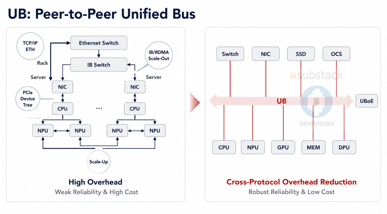
In traditional data centers, CPU, NIC, Ethernet switch, PCIe, RDMA, storage, memory, and accelerators are separated by multiple protocol layers. These protocols provide flexibility, but they also introduce latency, overhead, cost, and reliability challenges.
The direction of UnifiedBus is to reduce overhead between different protocols and make peer-to-peer communication more direct, allowing CPU, NPU, GPU, MEM, DPU, SSD, NIC, and switch to enter a more unified fabric.
This is the key to making the system behave like one machine.
But no matter how elegant the protocol layer is, it must eventually land on the physical layer. Data does not move by itself. It must pass through bumps, RDL, substrates, connectors, cables, fibers, lasers, modulators, photodiodes, retimers, switch fabrics, power delivery, and thermal systems.
Therefore, Hi-ONE’s role is very clear. It is not a replacement for UnifiedBus. It is a physical-layer tool that determines whether UnifiedBus can scale to larger distances.
If UnifiedBus is the language, Hi-ONE is the vocal cord and nervous system.
Without high-density optical I/O such as Hi-ONE, UnifiedBus will struggle to cross board, rack, rack-to-rack, and data center distances. Conversely, without a low-overhead system protocol such as UnifiedBus, Hi-ONE would only be a high-speed physical channel and would not automatically translate into effective AI workload throughput.
This is the most important part of Huawei’s current narrative. It is not a single-point breakthrough. It is an attempt to connect protocol, packaging, optics, thermal design, and system architecture into one route.
The Real Challenge Is Not Announcement, but Mass Production
The difficulty of near-packaged optical I/O has never been on PowerPoint slides. It is in mass production.
The first difficulty is optical coupling.
The alignment tolerance between a silicon photonics chip and a fiber array is extremely small. As channel count increases, coupling loss, reflection, polarization sensitivity, and temperature drift in any single channel can accumulate into system-level problems. To control coupling loss within 1 dB requires not only design capability, but also packaging equipment, active alignment, passive alignment, adhesives, reliability testing, and mass-production yield capability.
The second difficulty is thermal design.
The area near an AI ASIC may have the highest thermal flux density in the entire system. The closer the optical engine is to the ASIC, the more SerDes power can be reduced, but the more thermal stress increases. This is a classic trade-off: what you save electrically may be paid back through thermal design, reliability, and serviceability.
The third difficulty is testing.
High-channel-count optical engines are expensive to test. Wafer-level optical testing, known-good-die strategy, burn-in, BER testing, temperature cycling, fiber attach inspection, and optical power stability testing all affect production ramp speed.
The fourth difficulty is maintenance.
The advantage of traditional pluggable optical modules is that they can be removed and replaced when they fail. The problem with CPO and NPO is that once the optical engine moves closer to the package or the board-level core area, maintenance costs rise sharply. A data center is not a laboratory. When systems are deployed across thousands of racks, field failure handling directly affects TCO.
The fifth difficulty is supply chain.
Hi-ONE involves III-V light sources, silicon photonics chips, optoelectronic packaging, precision connectors, fiber arrays, substrates, test equipment, thermal management, and system software. If any one of these links is immature, the whole system can become constrained.
This is why the real test for Hi-ONE is not the demonstration sample. It is whether Hi-ONE can enter the real production design of Ascend SuperPOD.
Huawei Is Learning from NVIDIA, but the Road Is Harder
The core problem Huawei now faces is actually similar to NVIDIA’s: in the AI era, competition is no longer only chip competition. It is system competition.
NVIDIA’s strength is not only the GPU. It is the full-stack capability built from GPU, NVLink, NVSwitch, InfiniBand / Ethernet, CUDA, HGX, GB200 / GB300, rack-scale architecture, software ecosystem, and supply-chain integration.
If Huawei wants to build its own AI infrastructure route under a constrained environment, it cannot rely only on improving the performance of a single Ascend chip. It must build up the entire system layer, including:
Compute chips
HBM or alternative memory architectures
Chip-to-chip interconnect
Rack-scale interconnect;
UnifiedBus
SuperPOD
Optical I/O
Liquid cooling
Power delivery
Large-model training
Inference frameworks.
The real function of “Tao Law” is to provide a narrative shell for this route. It tells the market that when advanced manufacturing is constrained, performance growth will not stop. The battlefield simply shifts from transistor scaling to system scaling.
This direction is correct.
But a correct direction does not mean the engineering work is complete.
What Huawei truly needs to prove is whether, without full freedom across the global supply chain, it can use system engineering to recover part of the performance gap created by advanced-node constraints.
This is extremely difficult.
Because system-level optimization is not one single technological breakthrough. It requires every layer to work.

Conclusion: τ Is the Concept. Hi-ONE Is the Work.
Returning to the central point:
“Tao Law” clearly carries a strong strategic concept. It packages the survival problem of the post-Moore era into a new scaling law: the future is not only about shrinking L, but also about shrinking τ.
This idea is reasonable, but it should not be over-mythologized. The semiconductor industry has always been compressing time. In the past, we simply called it critical path optimization, RC delay reduction, memory latency reduction, SerDes power reduction, interconnect scaling, and system-level optimization.
What really matters is where Huawei anchors this narrative in concrete engineering tools.
Among all these tools, Hi-ONE is the one most worth tracking.
Because it directly faces the most brutal question in AI infrastructure: as chip counts continue to rise, how does data move? How is the system connected? How are latency and power reduced? Can optoelectronic packaging actually be mass-produced? How is failure handled? Can effective throughput be reflected in real large-model training and inference workloads?
τ is the concept. Hi-ONE is the real work.
The former explains the survival logic of the post-Moore era.
The latter confronts the hard reality of optoelectronic packaging, reliability, mass-production testing, protocol tolerance, and system deployment.
If Hi-ONE truly enters the actual system design of Ascend SuperPOD, and if it can close the engineering loop around built-in light source, 8Tbps optical I/O, low latency, high reliability, and serviceability, then it will not just be a PR term. It will become a critical piece of Huawei’s AI computing roadmap.
What we should wait for is not more naming of “laws.”
It is whether this piece can be physically installed into the system and actually work.
Thanks for reading SEMIVISION @_@! This post is public so feel free to share it.


PreviousNext