NVIDIA and Taiwan: Why the AI Revolution Is Turning the Island into the World’s AI Infrastructure Hub
NVIDIA and Taiwan: Why the AI Revolution Is Turning the Island into the World’s AI Infrastructure Hub
- Source: SemiVision
- Author: SEMIVISION
- Published: 2026-05-28T11:48:50+08:00
- URL: https://tspasemiconductor.substack.com/p/nvidia-and-taiwan-why-the-ai-revolution (1) NVIDIA and Taiwan: Why the AI Revolution Is Turning the Island into the World’s AI Infrastructure Hub


NVIDIA and Taiwan: Why the AI Revolution Is Turning the Island into the World’s AI Infrastructure Hub
Original Article By SemiVision Research [Reading time: 12 mins]

May 28, 2026
∙ Paid
NVIDIA and Taiwan: Why the AI Revolution Is Turning the Island into the World’s AI Infrastructure Hub
Jensen Huang has once again placed Taiwan at the center of the global AI map. His message was direct: Taiwan is not merely participating in the AI revolution; Taiwan is one of its epicenters.
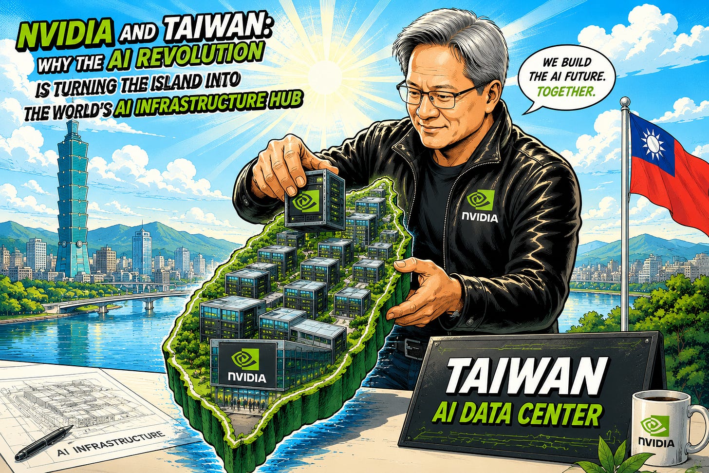
This statement should not be read only as a compliment. It is a strategic definition of Taiwan’s new role in the AI era. NVIDIA’s relationship with Taiwan is no longer just about chips, foundry services, or GPU assembly. It is about building the entire physical foundation of AI factories: silicon, advanced packaging, high-speed PCB, CCL materials, power delivery, thermal management, system integration, and data center infrastructure.

In other words, NVIDIA is not just buying components from Taiwan. NVIDIA is building the AI industrial stack with Taiwan.
From GPU Supply Chain to AI Factory Supply Chain
In the past, Taiwan’s semiconductor story was mainly centered on TSMC and advanced process technology. That story is still critical, but it is no longer sufficient.
The AI infrastructure cycle has expanded the boundary of value creation. A GPU is no longer just a chip. It is part of a rack-scale computing system. A rack is no longer just a server cabinet. It is becoming a high-density AI factory unit. As NVIDIA platforms move from GB200 and GB300 toward Rubin and Vera Rubin, the system boundary keeps expanding from chip to package, from package to board, from board to rack, and from rack to the entire data center power architecture.
This is why Taiwan matters so much. Taiwan is one of the few places in the world that can convert architecture into mass production at system scale.
1月31日
NVIDIA’s Taiwan Spending Is a Signal of Structural Dependency
According to Jensen Huang, NVIDIA’s annual procurement and spending in Taiwan has grown dramatically from roughly US$10–15 billion several years ago to around US$100 billion, and may move toward US$150 billion in the future. This is not just a larger purchase order. It is a reflection of how AI hardware value is being redistributed across the supply chain.
NVIDIA’s demand is no longer limited to wafers, GPUs, or accelerator cards. The company now needs full AI system manufacturing capacity. That includes advanced packaging, server platforms, high-speed networking, power modules, liquid cooling, rack integration, and eventually AI data center deployment.
This is the real meaning behind “Taiwan is booming.” Taiwan is no longer only a semiconductor manufacturing center. It is becoming the operating system of global AI hardware production.
EMC and ITEQ: Why CCL Materials Are Becoming AI Infrastructure Assets
The recent updates from Taiwan’s CCL leaders are particularly important. Elite Material Co., commonly referred to as EMC, and ITEQ, are both seeing strong demand from AI servers, 800G and 1.6T switches, high-speed computing platforms, and cloud data center infrastructure.
This matters because copper-clad laminate is not a glamorous component. It is not as visible as GPU, HBM, or CoWoS. But in the AI infrastructure era, CCL is becoming a performance-critical material.
As data rates move from 112G to 224G SerDes, the board is no longer just a passive carrier. It becomes part of the signal path. Material loss, dielectric stability, copper roughness, dimensional control, thermal reliability, and process consistency all directly affect system performance.
For AI servers and high-speed switches, low-loss materials are not optional. They are part of the architecture.

5月4日
Why “Full Capacity” at CCL Makers Is an Early Indicator
When EMC and ITEQ talk about strong demand visibility extending toward 2028, the market should pay attention. CCL suppliers sit upstream of PCB makers, ODMs, switch platform vendors, and system integrators. When material demand is locked in several years ahead, it often means the downstream platform roadmap is already being planned.
This is not a simple inventory restocking cycle. It is a platform migration cycle.
AI GPUs are becoming more powerful. HBM capacity is increasing. Switch bandwidth is moving to 800G and 1.6T. Rack power density is rising. PCB layer counts are increasing. Board sizes are becoming larger. Signal integrity requirements are becoming stricter.
All of these changes create structural demand for higher-end CCL materials.

2025年7月6日
The Real Bottleneck Is Moving from Compute to System Architecture
The first wave of the AI boom was defined by GPU availability.
The second wave is being defined by packaging capacity, especially CoWoS.
The next wave will increasingly be defined by system-level constraints: power delivery, thermal management, high-speed signaling, and data center infrastructure.
This is where Taiwan’s ecosystem becomes strategically important.
Taiwan does not only manufacture chips. It manufactures the full AI system. The island has TSMC for leading-edge silicon, ASE and SPIL for advanced packaging, major server ODMs for system integration, PCB and CCL companies for high-speed boards, thermal solution suppliers for liquid cooling, and power electronics companies such as Delta Electronics for power infrastructure.
This density of industrial capability is extremely difficult to replicate.
4月28日
NVIDIA’s 800V HVDC Roadmap Shows the Next Stage of AI Infrastructure
NVIDIA’s push toward 800V HVDC power architecture is one of the clearest signals that AI has entered a new phase. Traditional 54V rack power architectures were designed for kilowatt-scale systems. Future AI racks are moving toward hundreds of kilowatts and eventually megawatt-scale density.
This means AI infrastructure is no longer just a semiconductor problem. It is also an electrical infrastructure problem.
The industry now has to solve several problems simultaneously: how to deliver power efficiently into the rack, how to reduce conversion loss, how to minimize copper usage, how to manage heat, and how to keep the entire data center reliable under extreme power density.
This is why the AI supply chain is expanding from semiconductors into power semiconductors, power modules, busbars, liquid cooling, switchgear, and data center electrical systems.
AI workloads are growing exponentially, driving higher power demand in data centers. Traditional 54V in-rack power distribution was designed for kilowatt-scale racks and cannot support the megawatt-scale racks now entering modern AI factories.
Starting in 2027, NVIDIA is leading the transition toward 800V HVDC data center power infrastructure to support IT racks of 1MW and above. To accelerate adoption, NVIDIA is working with key partners across the data center electrical ecosystem, including:
Chip suppliers:Infineon, MPS, Navitas, ROHM, STMicroelectronics, Texas Instruments
Power system components:Delta, Flex Power, Lead Wealth, LiteOn, Megmeet
Data center power systems:Eaton, Schneider Electric, Vertiv
This initiative is designed to drive innovation and build a more efficient and scalable power delivery architecture for the next generation of AI workloads, while improving reliability and reducing infrastructure complexity.
Taiwan’s Role: Turning NVIDIA’s Architecture into Manufacturable Reality
NVIDIA designs the architecture, but Taiwan helps make it manufacturable.
This is the key point. NVIDIA’s AI roadmap is not only a chip roadmap. It is a system roadmap. Every new generation requires tighter coordination across foundry, packaging, substrates, PCB, CCL, power, cooling, mechanical design, and rack assembly.
Taiwan’s advantage lies in this coordination capability. Its suppliers are geographically close, technically experienced, and deeply integrated into each other’s development cycles. This allows NVIDIA to move faster from design concept to production ramp.
For AI hardware, speed of iteration is a competitive weapon. Taiwan gives NVIDIA that speed.
EMC, ITEQ, and the Second-Layer Revaluation of the AI Supply Chain
The market has already revalued the first layer of the AI supply chain: GPU, HBM, CoWoS, and AI server ODMs. But the second layer is still being repriced.
This second layer includes high-end CCL, low-loss materials, high-speed PCB, connectors, power modules, liquid cooling, busbars, and data center electrical infrastructure.
EMC and ITEQ are important because they represent this second-layer revaluation. Their products sit inside the physical highways that allow AI systems to move data at high speed and high reliability. As AI systems become larger and faster, these materials become more strategic.
In the 800G, 1.6T, and 224G SerDes era, material quality directly affects system feasibility. A lower-loss laminate can reduce design complexity. Better dimensional stability can improve yield. More reliable materials can reduce system failure risk.
This is why CCL is no longer just a cost item. It is becoming a strategic AI infrastructure material.

2025年10月27日
Taiwan Is Becoming an AI Industrial Island
Taiwan is becoming an AI industrial island. Its role is not limited to semiconductor fabrication. It is becoming the place where AI chips are transformed into deployable AI factories.
This includes wafer manufacturing, advanced packaging, high-speed substrates, CCL, PCB, server motherboards, switch boards, accelerator boards, rack integration, cooling systems, and power infrastructure.
The AI era is therefore expanding Taiwan’s strategic importance. In the smartphone era, Taiwan manufactured key components and devices. In the AI era, Taiwan is manufacturing the infrastructure layer of machine intelligence.
SemiVision View: NVIDIA and Taiwan Are Building the Physical Layer of AI
The key message is simple: NVIDIA cannot scale AI without Taiwan, and Taiwan’s semiconductor ecosystem is being reshaped by NVIDIA’s AI roadmap.
The first stage of the AI boom was about compute. The second stage is about infrastructure. This shift will continue to reprice the entire Taiwan supply chain.
TSMC remains the core. CoWoS remains critical. But the next layer of value will come from materials, boards, power, cooling, and system integration. EMC and ITEQ are early examples of this transition.
AI users do not only need tokens. They need electricity. AI servers do not only need GPUs. They need high-speed materials, reliable power delivery, advanced cooling, and manufacturable system architecture.
That is why NVIDIA’s Taiwan story is not just about procurement. It is about industrial co-development.
Taiwan is no longer only the world’s semiconductor foundry base. It is becoming the manufacturing backbone of the global AI factory.
5月14日
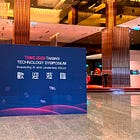
“Taiwan is booming!” NVIDIA CEO Jensen Huang repeatedly emphasized at the event.
He said he had been stressing Taiwan’s importance for many years and had long made clear that NVIDIA would continue increasing its investment in Taiwan. Around four to five years ago, NVIDIA’s annual spending in Taiwan was roughly US$10 billion to US$15 billion. Today, that figure has surged to around US$100 billion to US$150 billion.
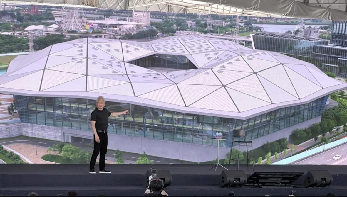
“Now I have been proven right, haven’t I?” Huang said with satisfaction. “A single company investing US$150 billion will inject enormous momentum into Taiwan’s ecosystem.”
This was the first time NVIDIA publicly revealed the design and timeline for its new Taiwan headquarters, NVIDIA Constellation. The campus will cover 700,000 square feet and is expected to break ground by the end of 2026, with completion and move-in scheduled for 2030. Huang said NVIDIA currently has around 1,000 employees in Taiwan, and the new headquarters will be able to accommodate up to 4,000 employees once completed.
“We want to become the first company in the world to replicate the design of our headquarters buildings across different parts of the world,” Huang said. He explained that NVIDIA’s new Taiwan headquarters will share the same design concept as the company’s next-generation headquarters building in the United States. Both projects are designed by renowned Taiwanese architect Kris Yao, who has worked with NVIDIA for more than a decade and is also one of the key architects behind NVIDIA’s global headquarters.
NVIDIA Constellation reflects the company’s core culture of transparency and openness. The building will feature a fully transparent exterior and will be composed of triangular and polygonal geometric elements.
Interestingly, the building will not include any elevators. Huang said frankly that he does not like elevators because elevators mean “waiting” — waiting to go up, waiting to go down, and wasting too much time. In addition, all parking will be placed underneath the building, allowing the entire site to maximize open space above ground.
The campus will also include skybridges, and one of the skybridges will even feature a bar. Huang jokingly said that, according to NVIDIA’s company culture, the bar is the most important facility in the entire building.
NVIDIA also added that it took 18 months to secure the land for this project, and the company expressed special gratitude to Taipei Mayor Chiang Wan-an and the Taipei City Government team for their strong support.
NVIDIA Constellation: An Architectural Proposal for an Open AI Campus in Taipei
From an architectural perspective, the four images present NVIDIA Constellation not simply as a corporate office, but as a low-rise, transparent technology campus embedded within Taipei’s urban landscape.
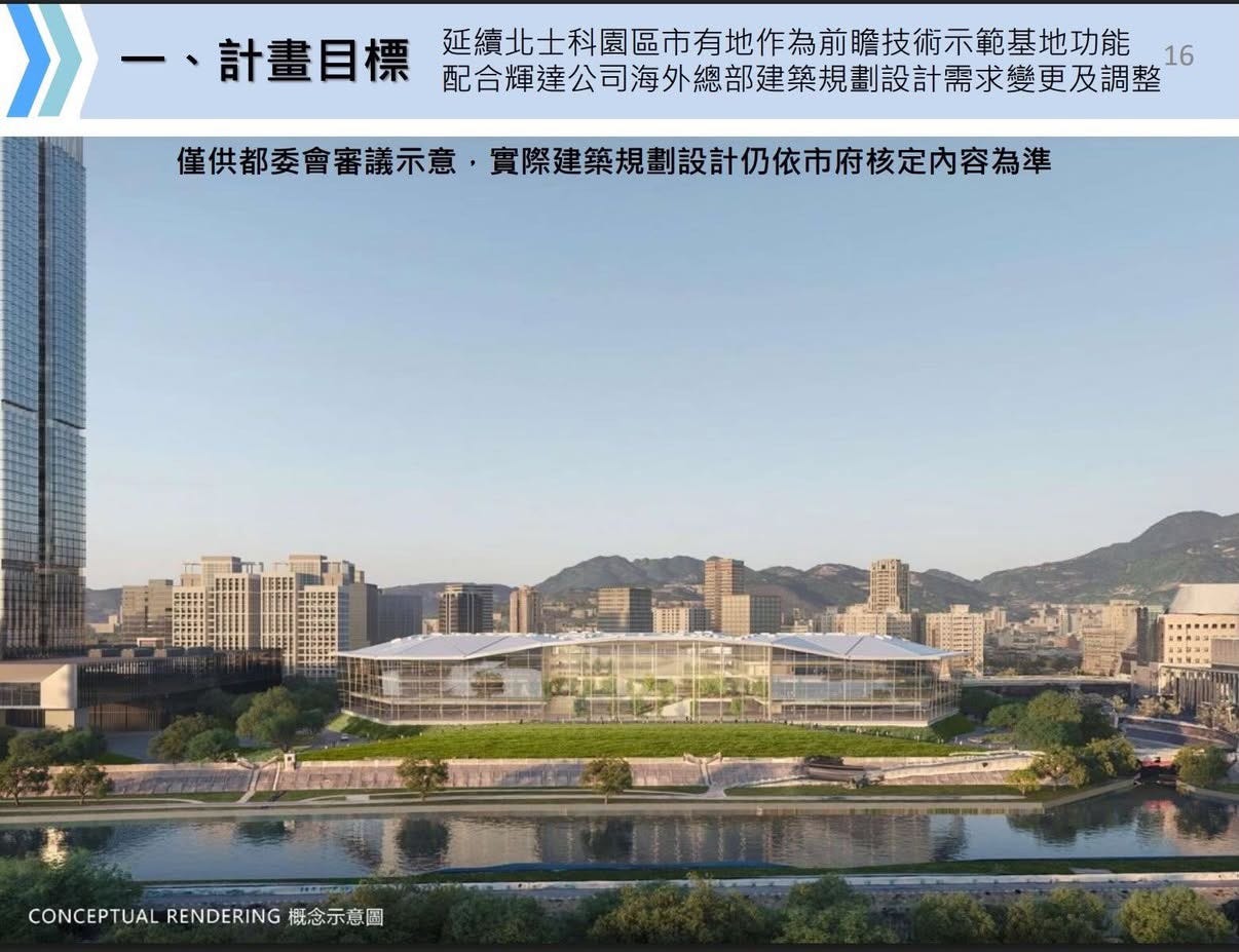
The building placed along the riverside, with mountains, city blocks, and public infrastructure forming the background. Instead of creating a dominant high-rise tower, the proposal adopts a horizontal and open campus form. The building appears light, transparent, and visually permeable, suggesting a workplace that is meant to connect with its surroundings rather than isolate itself from the city.
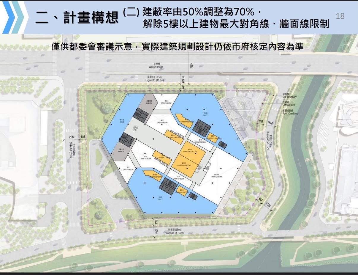
The building footprint is organized through a polygonal geometry, with multiple internal zones, courtyards, office areas, meeting spaces, connector spaces, and service cores. This layout creates a sense of movement and circulation. It is not a rigid rectangular office block; it is a spatial network designed for interaction, collaboration, and flexibility.

A building height of approximately35 to 45 meters, with around six above-ground levels and underground parking or service space below. The design keeps the building relatively low and broad, emphasizing horizontal connectivity. This is consistent with a campus-style headquarters model, where daily movement, visual connection, and open circulation are more important than vertical hierarchy.

NVIDIA Constellation sits beside the river and near existing urban landmarks, showing how the building may become part of the Beitou-Shilin Technology Park’s future skyline. The proposal also preserves generous setback areas and open space along the street, helping the project maintain a softer relationship with the surrounding public realm.
Overall, these four images suggest an architectural concept built around transparency, openness, geometry, and urban integration.
NVIDIA Constellation is presented as a new type of AI-era headquarters: not a sealed corporate tower, but a visible, accessible, and collaborative campus that reflects the company’s culture and Taiwan’s growing role in the global technology ecosystem.
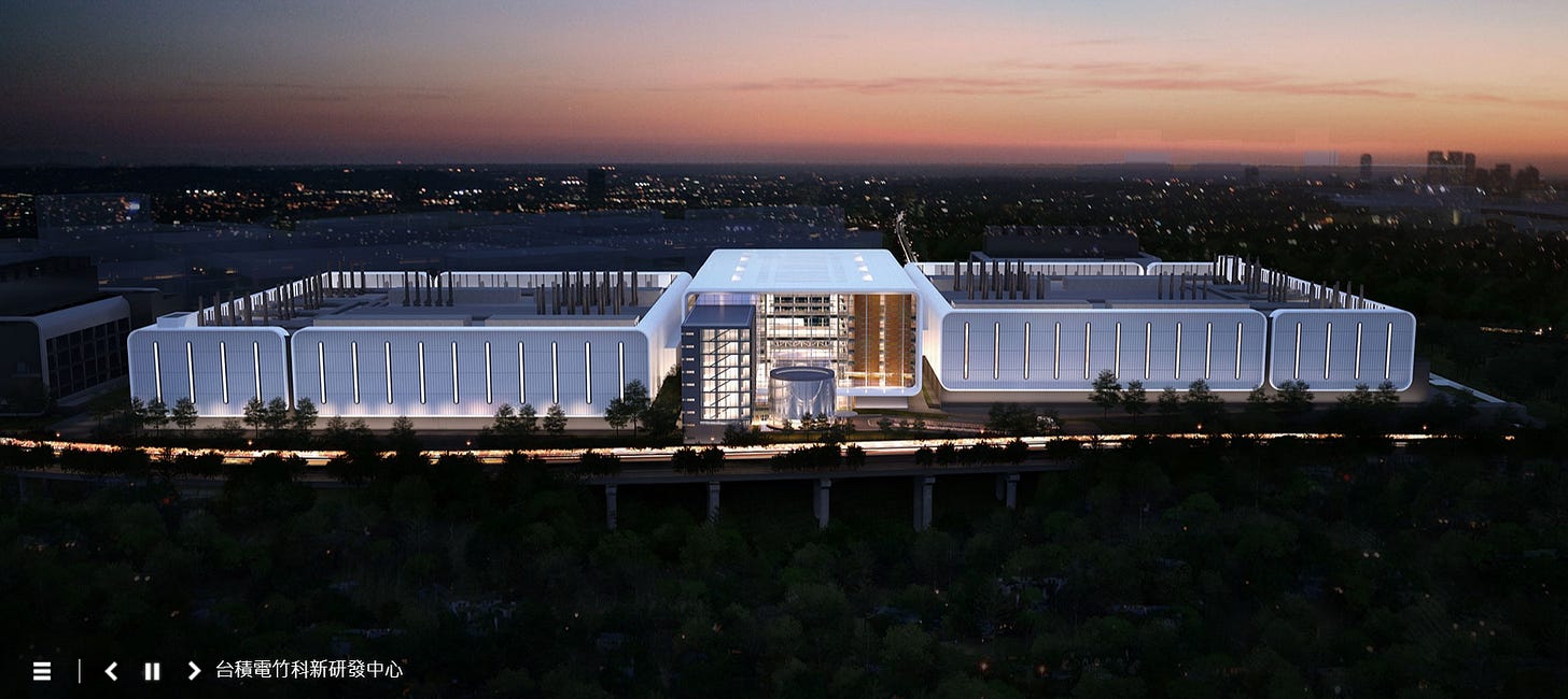
The TSMC Global R&D Center, located in Baoshan, Hsinchu Science Park, was designed by renowned Taiwanese architect Kris Yao and his firm, Kris Yao | Artech.
The building was inaugurated in mid-2023. For this major technology hub, which can accommodate more than 7,000 R&D engineers, Kris Yao introduced a strong sense of human warmth and spatial ingenuity.
One key feature is its transparent interactive space. Instead of reinforcing the cold separation traditionally associated with cleanrooms and office areas, Yao designed the enclosed wafer transport tracks as glass corridors. This allows employees and executives moving through the bright central atrium and surrounding walkways to see one another’s activities, creating a stronger sense of shared purpose and collective R&D spirit.
The building also emphasizes natural lighting and ecological design. It meets green building standards and uses the atrium to bring in natural daylight, water features, and a more relaxed spatial atmosphere. Even the basement cafeteria is equipped with light wells, creating a more harmonious and human-centered working environment.
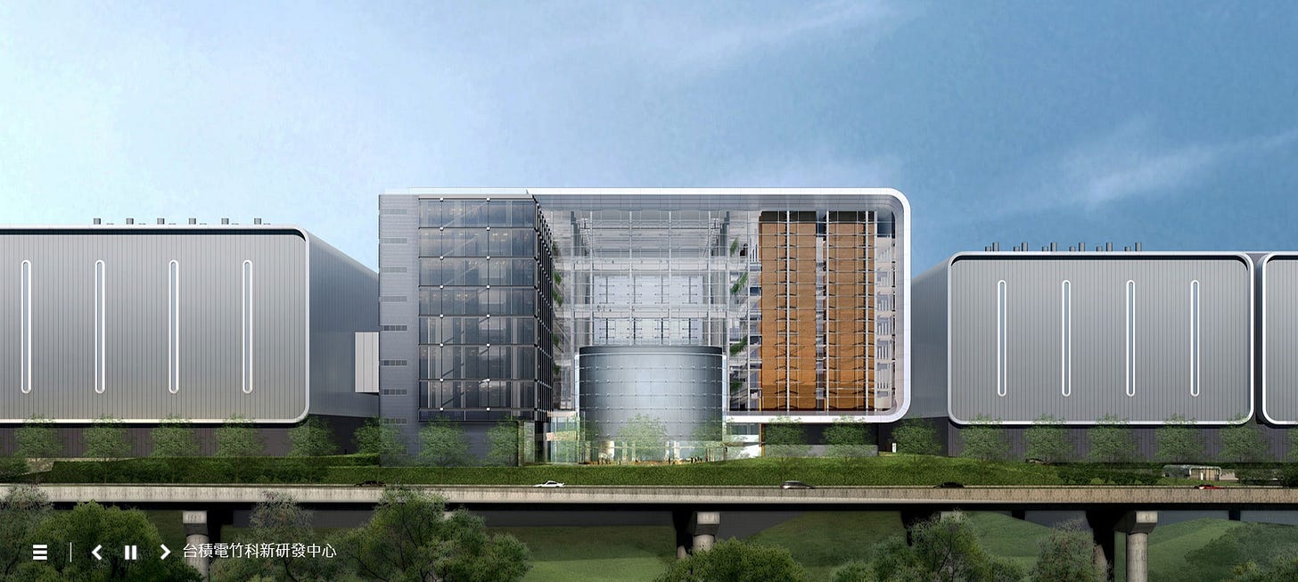
Kris Yao is highly regarded for his work in technology facility design. In addition to TSMC’s Global R&D Center, he has also been involved in the design of TSMC’s Arizona fab in the United States, its Nanjing fab, and the new NVIDIA headquarters in Beitou-Shilin Technology Park, known as NVIDIA Constellation.
Thanks for reading SEMIVISION @_@! This post is public so feel free to share it.


PreviousNext