ASML’s EUV Power Strategy: More Wafers per Kilowatt-Hour, Not Just Smaller Nodes
ASML’s EUV Power Strategy: More Wafers per Kilowatt-Hour, Not Just Smaller Nodes
- Source: SemiVision
- Author: SEMIVISION
- Published: 2026-05-28T09:24:46+08:00
- URL: https://tspasemiconductor.substack.com/p/asmls-euv-power-strategy-more-wafers (1) ASML’s EUV Power Strategy: More Wafers per Kilowatt-Hour, Not Just Smaller Nodes


ASML’s EUV Power Strategy: More Wafers per Kilowatt-Hour, Not Just Smaller Nodes
Original Article By SemiVision Reserach [Reading time: 21 mins]

May 28, 2026
∙ Paid
ASML’s EUV Power Strategy: More Wafers per Kilowatt-Hour, Not Just Smaller Nodes

The semiconductor industry is entering a new constraint in capacity expansion: power.
In the past, when the industry discussed advanced process technology, the core issues were yield, capacity, mask layers, equipment lead times, and capital expenditure. But in the AI era, another more fundamental bottleneck is emerging: electricity.
AI servers, HBM, advanced packaging, and high-end logic chips are driving a new global investment cycle in wafer fabs. The problem is that a fab does not expand simply because it has land, capital, and equipment. When the power demand of an advanced fab approaches that of a small city, and when EUV, etching, deposition, metrology, cleanrooms, and utility systems are all added together, energy is no longer just an operating cost. It becomes a precondition for capacity expansion.
This is why ASML’s recent sustainability briefing in Taiwan may appear to be about ESG and energy saving, but its deeper significance is tied to the systemic bottlenecks of advanced process expansion.
Grace Wang, General Manager of ASML Taiwan, stated that semiconductors are a critical foundation for digitalization and AI development, which means the industry must assume greater responsibility in energy and sustainability. ASML will continue to support the long-term development of the semiconductor industry through technology innovation, manufacturing efficiency improvements, and close collaboration with customers and supply chain partners.

The key word here is not only “sustainability,” but “technology innovation.”
For wafer fabs, meaningful energy saving does not come merely from using less air conditioning in offices or sourcing more renewable power for buildings. The real issue is whether the most critical process equipment can produce more wafers under the same power conditions.
ASML’s numbers are important: EUV energy consumption per wafer is expected to fall from 12.8 kWh in 2018, during the NXE:3400 era, to 2.8 kWh by 2031 with the NXE:4600. In other words, the EUV energy consumed per wafer will be reduced to around 22% of the 2018 level — almost one-fifth.
This is not simply about making the machine “more power efficient.” It is about redesigning the efficiency logic of the entire lithography system.
The Real Issue Is Not How Much Less Power the Tool Uses, but How Many Wafers It Can Produce with the Same Power Budget
To understand ASML’s EUV energy roadmap, one cannot look only at the total power consumption of the machine. Two indicators must be examined together: Absolute Power, meaning the tool’s power consumption as a percentage of the 2018 baseline, and Energy per Wafer, meaning how much energy is allocated to each wafer.
These two numbers do not move in exactly the same direction. That difference is the key to the entire roadmap.

The NXE:3400 in 2018 serves as the baseline. At that time, the tool’s absolute power was set at 100%, energy consumption per wafer was 12.8 kWh, and throughput was around 112 wafers per hour. By 2031, with the NXE:4600, ASML expects absolute power to decline to 77%. In other words, the total power consumption of the tool itself will fall by only about 23%. If we look only at this number, the improvement may not appear dramatic.
But during the same period, energy per wafer falls from 12.8 kWh to 2.8 kWh. The reason is that NXE:4600 can process around 400 wafers per hour, nearly 3.6 times the 2018 level.
This means ASML is not simply turning EUV into a “low-power machine.” It is enabling one machine to process far more wafers within a similar power budget. For wafer fabs, this has far greater strategic significance than simply reducing the rated power of a tool.
When fabs plan capacity expansion, power applications are usually based on the combined load of equipment, facilities, and utility systems. But the real manufacturing economics depend on how much power cost is allocated to each wafer. When the same EUV tool can process more wafers per hour, electricity consumption no longer rises in direct proportion to wafer output. This creates new flexibility in capacity expansion.
This is also why High-NA EUV tools can still reduce energy per wafer even though they are physically larger, more complex, and consume more power. The NXE:4200G and NXE:4200H have absolute power ratios of 94% and 96%, respectively, almost returning to the 2018 power level. But because their throughput rises to around 300 and 330 wafers per hour, their energy consumption per wafer can still be reduced to roughly one-third of the 2018 level.
In other words, against the backdrop of AI-driven demand for advanced process capacity, the key energy-saving question for EUV is not “how much less electricity does one tool consume?” but “how many wafers can one kilowatt-hour expose?”

Below we will share:
Sleep Mode: Stopping EUV from Burning Power When It Is Not Actually Working
Hydrogen Recycling and 32°C Cooling Water
The Real Energy Value of High-NA EUV Is Not That Each Tool Uses Less Power, but That the Whole Fab Runs Fewer Multiple-Patterning Steps
Taiwan’s Role: EUV Energy Reduction Is Not a European Sustainability Topic, but a Real Constraint in Taiwan’s Advanced Process Expansion
EUV Energy Reduction Will Reshape the Cost Structure of the AI Chip Supply Chain

Sleep Mode: Stopping EUV from Burning Power When It Is Not Actually Working
The first engineering measure issleep mode.
An EUV tool is not truly exposing wafers every second. Wafer exchange, alignment, stage movement, intervals between exposures, and optical system preparation all take time. These are not effective exposure periods. If all subsystems inside the tool continue running at full power during these gaps, a large amount of energy is wasted.
Starting from NXE:3600, ASML gradually turned questions such as “which subsystems can rest,” “when power can be reduced,” and “whether the system can quickly return to a stable state after resting” into an engineering control logic.
The NXE:3600 introduced RF Sleep Mode in 2021. An EUV tool contains multiple radio-frequency power systems that require continuous power. In the past, even during wafer exchange or non-exposure intervals, these systems still had to maintain relatively high power states. RF Sleep Mode allows these systems to enter a low-power state during short idle periods, reducing ineffective energy consumption.
This step reduced absolute power from 100% to 86%, lowered energy per wafer from 12.8 kWh to 7.7 kWh, and increased throughput to around 160 wafers per hour.

By 2023, the NXE:3800E added more granular control on top of sleep mode. One improvement was Reduced Fire Between Exposures, meaning fewer laser shots during intervals between exposures. EUV light is generated by using a CO2 laser to strike high-speed tin droplets, producing 13.5 nm EUV light. If the laser continues firing at high frequency during non-exposure periods, it creates unnecessary energy consumption and thermal load. Reducing laser output between exposures cuts this ineffective energy use.
The second improvement was LSM Sleep Mode, which allows specific optical subsystem modules to enter a low-power state during non-exposure periods. This type of energy saving is not a simple switch. It requires coordination among the light source, optical modules, vacuum environment, thermal stability, and exposure cadence.
Together with a High Brightness Source that improves light-source brightness and exposure efficiency, NXE:3800E increased throughput to around 230 wafers per hour, reduced absolute power to 79%, and further lowered energy per wafer to 5.2 kWh.
The planned NXE:3800F in 2026 will add H2 Sleep Mode. EUV tools require hydrogen to maintain cleanliness in the source and optical path. In traditional designs, the hydrogen system often maintains a relatively stable continuous flow. H2 Sleep Mode allows the hydrogen system to reduce operating intensity during non-critical periods, further cutting unnecessary consumption.
More importantly, by 2031, the NXE:4600 will move beyond putting selected modules to sleep. ASML’s logic will shift toward “System ON when needed,” meaning full-machine-level, demand-based activation.
This means EUV power management will evolve from “the system is always on, with partial load reduction” to “the system enters a high-power state only when it is truly needed.” This is not conventional energy saving. It is a change in equipment control philosophy.
Hydrogen Recycling and 32°C Cooling Water: The Savings Are Not Only on the Tool’s Bill, but Across the Entire Fab Utility System
The second and third engineering measures are hydrogen recycling and higher cooling-water temperature.
These two measures may not appear to be part of EUV exposure itself, but they matter greatly to total fab energy cost. An advanced EUV tool does not operate in isolation. It is connected to hydrogen supply, cooling water, vacuum systems, fab utilities, and safety systems. Real energy consumption occurs not only inside the equipment, but also in the facility infrastructure around it.
First, hydrogen.
The basic mechanism of an EUV light source is to use a CO2 laser to hit high-speed tin droplets, turning the tin into hot plasma and generating EUV light at a wavelength of 13.5 nm. But this process produces tin debris, residues, and contamination risks. To protect optical components, hydrogen must be continuously introduced into the system to help remove residues and keep the optical path clean.
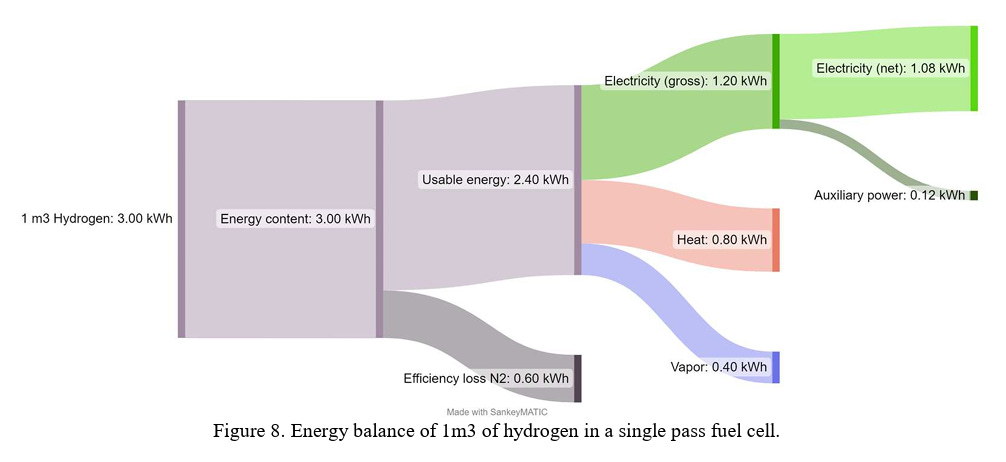
Traditionally, hydrogen is discharged after use. This means the fab must continuously supply high-purity hydrogen. Starting from NXE:3800F, ASML will introduce hydrogen recycling, allowing used hydrogen to be purified and reintroduced into the system, thereby reducing the need for fresh hydrogen supply.
What is saved here is not only the gas itself. It also includes the energy required for high-purity gas supply, compression, processing, safety management, and emission handling. In other words, hydrogen recycling reduces the load on the fab utility system.

Now consider cooling water.
EUV tools generate substantial heat during operation, which must be removed by cooling water. Many high-precision tools traditionally require low-temperature cooling water in the 12°C to 15°C range, which usually depends on energy-intensive chillers. Chillers are among the most power-hungry parts of a fab’s utility system. This is especially true in high-temperature or high-humidity regions such as Taiwan, Singapore, and Arizona, where cooling systems themselves become major power loads during fab expansion.
The NXE:3800F raises the cooling-water temperature specification to 32°C. On the surface, this looks like a simple change in cooling-water temperature. In reality, it opens up more infrastructure options for fabs. In many conditions, 32°C cooling water can be supported by cooling towers or lower-energy cooling solutions, rather than relying fully on high-power chillers.
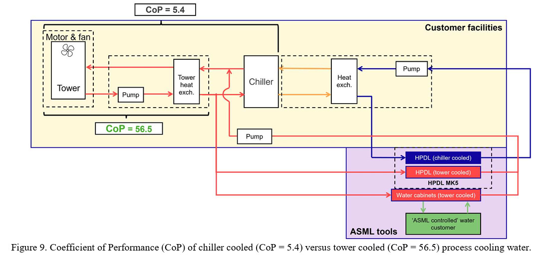
The electricity saved here may not appear directly on the EUV tool’s own power meter, but it will show up on the utility bill of the entire fab. For fab operators, this is closer to actual operating reality than tool-level power saving alone, because the capacity of the utility system often determines whether a fab site can support more equipment.
Therefore, the significance of NXE:3800F is not a single-point improvement. It reduces both tool-side and facility-side load. ASML’s reduction of energy per wafer from around 5.2 kWh on NXE:3800E to roughly 4.2 kWh on NXE:3800F is enabled by the combined effect of sleep mode, hydrogen management, and cooling-system optimization.

4月9日
The Real Energy Value of High-NA EUV Is Not That Each Tool Uses Less Power, but That the Whole Fab Runs Fewer Multiple-Patterning Steps
If one looks only at the individual tool, High-NA EUV may not intuitively appear energy efficient. It is larger, more complex, and more expensive, and it places higher demands on fab utilities, vibration control, thermal management, and service support.
But the energy-saving logic of High-NA EUV does not sit at the single-tool level. It sits at the level of the full fab process flow.
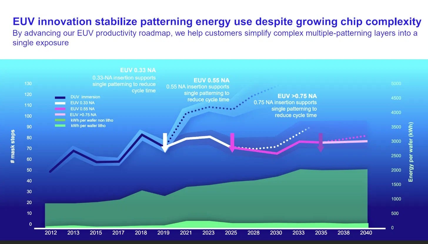
The complexity of advanced logic processes continues to rise. Each new node requires more mask layers, higher pattern density, and tighter linewidth control. Before EUV became widely adopted, many critical layers had to be produced through DUV immersion lithography combined with multiple patterning. In other words, the same circuit layer might need to be split into multiple exposures, etch steps, and alignment cycles before the required pattern could be defined.
This creates three problems.
First, tool count increases. Multiple patterning means more DUV tools and more exposure steps. Second, process cycle time becomes longer. Each additional exposure adds alignment, metrology, and process risk. Third, total fab energy consumption rises, because every exposure step comes with equipment, utility, and cleanroom loads.
The greatest value of 0.33 NA EUV was that it compressed some layers previously requiring multiple DUV exposures into single EUV exposures. It did not simply replace one DUV tool. It compressed multiple tools, multiple process steps, and multiple waiting periods into a shorter and cleaner process flow.
High-NA EUV extends this logic. When 0.33 NA EUV begins to require multiple exposures for certain denser patterns, 0.55 NA High-NA EUV provides higher resolution, allowing more critical layers to return to single-exposure patterning.
Therefore, the energy-saving nature of High-NA EUV lies in process compression. It allows one high-end tool to replace the workload previously handled by multiple tools, multiple exposures, and multiple process segments. Although the power consumption of a single High-NA EUV tool is not low, if it can reduce total exposure steps, shorten process cycle time, reduce rework, and improve yield, overall energy consumption may still decline.
This is why ASML emphasizes that the introduction of High-NA EUV can simultaneously improve yield, shorten production cycle time, and lower both unit wafer manufacturing cost and energy consumption. That statement captures the core logic of semiconductor manufacturing: energy saving is not an isolated metric. It is tied to yield, cycle time, mask steps, equipment count, and capacity efficiency.

The more complex AI chips become, the less meaningful it is to look only at the power consumption of a single tool. The real question is how much energy the entire process line consumes to produce one qualified wafer.
Taiwan’s Role: EUV Energy Reduction Is Not a European Sustainability Topic, but a Real Constraint in Taiwan’s Advanced Process Expansion
ASML’s decision to discuss sustainability in Taiwan is not coincidental.
Taiwan is one of the world’s most important EUV user bases and the core hub for AI chips, advanced logic, HBM-related processes, and advanced packaging. As TSMC continues expanding 2 nm, A16, A14, A12/A13, and advanced packaging capacity, Taiwan faces not a simple capacity issue, but a combined pressure from land, water, power, talent, equipment service, and supply chain density.
ASML plans to recruit around 1,000 new employees in Taiwan this year, covering customer support, manufacturing, and supply chain roles. This indicates that ASML’s role in Taiwan is no longer just that of an equipment supplier. It has become part of the advanced process mass-production system.
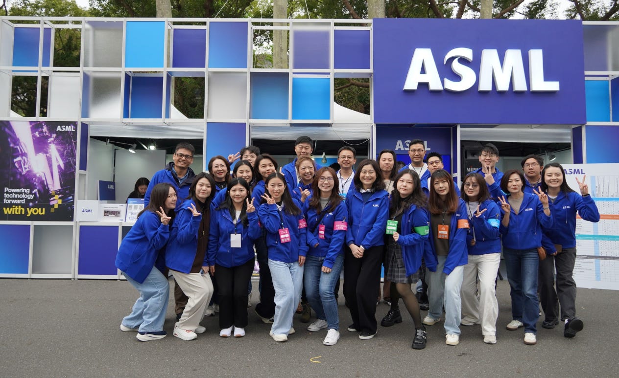
ASML’s 2026 campus recruitment officially kicked off today! The first stop in March will be the NTU Campus Recruitment Fair.
First, extending the life of installed equipment is itself a form of resource efficiency. Semiconductor equipment is not a consumer product that can simply be discarded after use. Each EUV, DUV, metrology, or inspection tool contains large numbers of high-value components and precision systems. Whether these tools can be refurbished and extended directly affects capital efficiency and supply chain pressure.
This is especially important for Taiwan, where advanced process capacity density is extremely high and new fab sites cannot expand power, water, land, and environmental approvals without limits. Under these conditions, improving output efficiency per tool, per kilowatt-hour, and per square meter of fab space will become a critical metric for the next stage of wafer-fab competitiveness.
EUV Energy Reduction Will Reshape the Cost Structure of the AI Chip Supply Chain
From a supply chain perspective, ASML’s reduction of EUV energy consumption per wafer to one-fifth of the 2018 level is not merely an ESG achievement. It is part of the AI chip cost structure.
AI chip costs are rising across the board. Advanced-process wafer prices are increasing. HBM prices are rising. CoWoS and advanced packaging capacity remain tight. Substrates, interposers, materials, and thermal solutions are all upgrading simultaneously. If lithography energy consumption does not fall, the electricity cost and utility investment required for fab expansion will be further added to chip costs.
Conversely, if EUV energy per wafer continues to decline, fabs can support higher output under the same power conditions. This produces three outcomes.
First, unit manufacturing cost at advanced nodes can decline. EUV energy is only one part of the cost structure, but when equipment depreciation, masks, materials, electricity, utilities, and cycle time are all added together, lower energy per wafer still has real economic significance.
Second, fab expansion becomes more flexible. If the same power allocation can support more wafer output, fabs reduce some of the pressure tied to local power supply and infrastructure constraints.
Third, the economic case for High-NA EUV becomes easier to justify. High-NA EUV tools are extremely expensive, and the industry has long focused on their return on investment. But if High-NA EUV can reduce multiple patterning, improve yield, shorten cycle time, and lower energy per wafer, the economic calculation should not be based only on the price of one tool. It must be evaluated at the level of the entire process module.
This is why SemiVision believes that future advanced-node competition will not revolve only around the question of “who introduces High-NA first.” It will evolve into a broader question: who can turn High-NA adoption into a system-level advantage through process compression, energy efficiency, yield improvement, and faster capacity ramp-up?

4月17日
Conclusion: In the AI Era, Advanced Process Competition Is Entering the Age of “How Much Compute Can Be Produced per Kilowatt-Hour”
From NXE:3400 to NXE:4600, ASML is using thirteen years to reduce EUV energy consumption per wafer from 12.8 kWh to 2.8 kWh. The significance of this curve is not just equipment-level energy saving. It means the capacity model of advanced process manufacturing is being rewritten.
In the past, the semiconductor industry often measured technological progress by transistor cost per square millimeter. In the AI era, another hidden metric may become increasingly important: how much effective wafer output can be supported by each kilowatt-hour of electricity, and ultimately how much AI compute can be produced from that energy.
The three engineering measures behind EUV energy reduction — sleep mode, hydrogen recycling, and higher cooling-water temperature — may look like equipment details. But in reality, they correspond to three levels of efficiency improvement: energy saving along the time axis, reuse of consumable resources, and lower load on fab utility systems. Together with the process compression enabled by High-NA EUV, ASML is turning lithography from a single process tool into a core control point for fab energy efficiency.
For Taiwan, this is especially important. Taiwan is not only home to major EUV customers, but also the global hub for AI chip manufacturing and advanced packaging. Whether Taiwan can continue to absorb advanced process expansion in the AI era depends not only on TSMC’s process capability, but also on whether the entire equipment, utility, energy, materials, and service ecosystem can improve efficiency together.
In other words, semiconductor competition in the AI era is no longer only about who can achieve smaller linewidths. It is about who can use less energy, shorter cycle time, and higher yield to produce more high-value wafers at scale.
ASML’s EUV energy curve is one of the most easily underestimated but most important underlying signals in this competition.

4月28日

- Improving EUV Source Efficiency: Generating More EUV Light with the Same Energy Input
One of the largest sources of energy consumption in an EUV lithography system is the light source. EUV light is not generated like conventional light. Instead, a high-power CO₂ laser strikes high-speed tin droplets, turning the tin into plasma and generating EUV light at a wavelength of 13.5 nm.
The challenge is that EUV light loses energy as it passes through the optical system. After multiple reflections, only a very small portion of the originally generated EUV light actually reaches the wafer surface. This means that the higher the source efficiency, the faster the system can expose wafers without significantly increasing total power consumption.
ASML improves this by enhancing the efficiency of the CO₂ laser and tin droplet system. This includes increasing the repetition rate of the laser and droplet generator, optimizing the pre-pulse to shape the tin droplet for better infrared absorption, and improving the drive laser architecture. As a result, EUV source power increased from around 200W in 2016 to around 600W in 2022, while energy consumption remained nearly constant. This improved source efficiency by roughly 280% from NXE:3400 to NXE:3800.
Simply put: the goal is not only to make the tool consume less electricity, but to generate more usable EUV light from the same amount of power, thereby increasing wafer output per hour.
- Sleep Mode: Reducing Power Consumption When the Tool Is Not Exposing Wafers
An EUV tool is not exposing wafers every second. Wafer exchange, lot scheduling, alignment, and process waiting time all create short idle periods. In the past, even when the tool was not actively exposing wafers, many subsystems still operated at high power, wasting energy.
ASML’s Sleep Mode allows the tool to reduce power consumption during idle periods without affecting wafer output. This requires close coordination between the fab automation system and the EUV tool control system to determine when the tool can enter sleep mode and when it needs to wake up.
The most important subsystem is the CO₂ drive laser. RF electrodes can be switched off and restarted relatively quickly. After a short calibration, stable EUV output can be restored within a few minutes. The more difficult part is the turbo blower and other thermally sensitive components. Turning them off and on can create thermal gradients and mechanical deformation, affecting laser alignment and pump efficiency. ASML therefore has to improve mechanical design and inline calibration to reduce wake-up time to the level of only a few minutes.
Simply put: Sleep Mode is not about shutting the tool down for a long time. It is about quickly reducing load during short idle windows and rapidly recovering, so the EUV system does not waste power while waiting.
- Hydrogen Recovery / Reuse: Reducing the Energy Burden of Gas Supply and Vacuum Systems
The tin plasma inside an EUV light source generates high-energy ions and tin debris. If not properly managed, these particles can contaminate the collector mirror and vessel walls. To reduce contamination, EUV systems use hydrogen as a buffer gas to slow down high-energy particles and carry contaminants toward the exhaust system.
This hydrogen supply and exhaust treatment system itself consumes significant energy. According to ASML’s data, hydrogen generation and the vacuum system required to remove contaminated hydrogen account for around 20% of total EUV system energy consumption.
Hydrogen recovery can take two paths. One is to recover the energy contained in hydrogen through a fuel cell. The other is to purify the hydrogen and feed it back into the EUV system, reducing net hydrogen consumption. However, the fuel-cell option is affected by nitrogen mixing, single-pass operation, and pump losses for pressurization, resulting in an overall system efficiency of around 36%. By comparison, hydrogen recycling more directly reduces the burden of high-purity gas supply and exhaust treatment in the fab.
Simply put: hydrogen recovery saves more than just hydrogen itself. It reduces the energy consumed across high-purity gas production, delivery, compression, vacuum exhaust, and contamination treatment.
- Using 32°C Cooling Water: Shifting Part of the Cooling Load from Chillers to Cooling Towers
EUV tools require substantial cooling, but not every subsystem needs low-temperature cooling water at 10°C to 18°C. Traditional low-temperature cooling water usually depends on energy-intensive chillers, which are among the most power-hungry parts of a fab’s utility system.
ASML’s approach is to cool less temperature-sensitive subsystems, such as large parts of the drive laser, with water at temperatures up to 32°C. This allows the fab to use cooling towers instead of relying entirely on chillers. According to ASML, when the drive laser cooling water temperature is raised to 32°C, total cooling power, including pumps, can be reduced by around 75%.
In addition, the electronics cabinets in High NA systems have been shifted from air exhaust cooling to indirect water cooling using 32°C cooling water, reducing cabinet cooling energy consumption by about 50%.
Simply put: 32°C cooling water is not merely a relaxed specification. It allows fabs to reduce reliance on power-hungry chillers and use more efficient cooling towers, saving electricity at the fab utility level.
- Reducing Multiple Patterning: Lowering Fab-Level Energy Consumption Through Process Flow Simplification
EUV energy savings do not only happen inside a single tool. They also occur across the entire process flow. As semiconductor nodes advance and patterns become finer, conventional DUV lithography often requires multiple exposures and repeated process iterations to define a single layer. Each additional exposure means another tool run, another alignment step, another metrology step, and often additional etch or cleaning processes. All of this consumes more energy.
The value of EUV and future High NA EUV is that higher resolution can compress some patterns that previously required multiple exposures into fewer exposures, or even a single exposure. ASML notes that improving lithography resolution and adopting EUV can reduce process steps, thereby lowering the lithography-related and process-related energy needed to manufacture devices.
Simply put: EUV itself may be a high-power tool, but if it can replace multiple DUV exposures and process steps, the total energy consumption of the fab can decline.
- Using Recycled Materials and Equipment Refurbishment: Reducing the Carbon Footprint of Hardware Itself
In addition to energy consumed during tool operation, the hardware itself also carries an embedded carbon footprint. EUV systems are composed of a large number of components involving materials, manufacturing, and transportation. In a pilot study on the EUV base frame, ASML found that material was one of the largest contributors to carbon footprint. If recycled aluminum is used instead of virgin aluminum, the carbon footprint of that module can be reduced by around 86%.
This means ASML’s energy-saving and carbon-reduction strategy is not limited to tool operation. It also extends to equipment manufacturing, component materials, refurbishment, repair, and reuse. For wafer fabs, extending equipment life and reusing parts are also important paths to reducing resource consumption.
Simply put: energy saving should not be measured only by electricity consumption after the tool is plugged in. It should also include the full lifecycle of the equipment, from materials and manufacturing to transportation, maintenance, and reuse.
ASML’s EUV energy-saving methods can be divided into three levels. The first is internal tool efficiency improvement, such as source efficiency and Sleep Mode. The second is reduction of fab utility load, such as hydrogen recovery and 32°C cooling water. The third is process flow compression and lifecycle carbon reduction, such as reducing multiple patterning, equipment refurbishment, and recycled materials.
The real point is not simply how much less electricity a single tool consumes. The real question is how much effective wafer output each kilowatt-hour can support.
Thanks for reading SEMIVISION @_@! This post is public so feel free to share it.


PreviousNext