VIS’s AI Moment: Why Mature-Node Specialty Processes Are Becoming Strategic Again
VIS’s AI Moment: Why Mature-Node Specialty Processes Are Becoming Strategic Again
- Source: SemiVision
- Author: SEMIVISION
- Published: 2026-05-27T11:32:43+08:00
- URL: https://tspasemiconductor.substack.com/p/viss-ai-moment-why-mature-node-specialty (1) VIS’s AI Moment: Why Mature-Node Specialty Processes Are Becoming Strategic Again


VIS’s AI Moment: Why Mature-Node Specialty Processes Are Becoming Strategic Again
Original Article By SemiVision Research [Reading time: 25 mins]

May 27, 2026
∙ Paid
VIS’s AI Moment: Why Mature-Node Specialty Processes Are Becoming Strategic Again
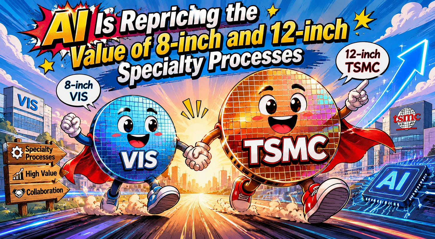
In Taiwan’s semiconductor map, TSMC is usually understood as the global leader in advanced process technology, while Vanguard International Semiconductor Corporation, or VIS, is often categorized as a mature-node foundry. This classification is directionally correct, but it is not sufficient.

VIS is not simply a smaller version of TSMC. Nor is it merely another 8-inch wafer foundry competing in the low-growth mature-node market. Its strategic position is much more specific: VIS is a long-standing TSMC-affiliated company, an independent foundry, and a key platform for preserving and monetizing mature-node value within Taiwan’s semiconductor ecosystem.
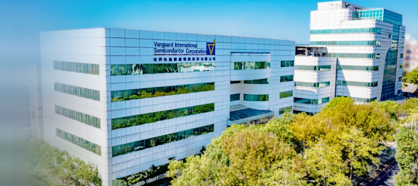
The relationship between TSMC and VIS cannot be explained by the simple language of parent and subsidiary. Legally and operationally, VIS is not a TSMC subsidiary. TSMC has long been its largest single shareholder, with a stake around the high-20% range, but it does not hold majority control. VIS is independently listed, has its own board, its own management team, and its own capital allocation discipline.
However, it would also be inaccurate to describe VIS as just another unrelated foundry. Its history, technology roots, customer trust, and strategic role are closely tied to TSMC. The better way to understand VIS is this: it is TSMC’s non-subsidiary ally in mature and specialty processes. It sits outside TSMC’s direct operating structure, but inside the broader strategic logic of Taiwan’s semiconductor division of labor.
This distinction matters. As TSMC moves deeper into 3nm, 2nm, A16, CoWoS, SoIC, and next-generation AI infrastructure, it must continuously reallocate capital, talent, cleanroom space, and management attention toward the highest-value frontier. But the semiconductor world does not run only on advanced logic. Power management ICs, display drivers, MOSFETs, IGBTs, analog ICs, mixed-signal devices, MEMS, sensors, protection devices, and interposer-related processes remain essential to every system.
That is where VIS becomes strategically important.
TSMC defines the height of Taiwan’s semiconductor industry. VIS helps support its thickness.
From DRAM Policy Mission to Mature-Node Foundry Platform
To understand VIS properly, we need to go back to Taiwan’s semiconductor industrial history in the 1990s.
At that time, Taiwan had already built strong capabilities in PC manufacturing and electronics assembly, but key memory components were still heavily dependent on imports. To address this weakness, Taiwan’s Industrial Technology Research Institute promoted the Submicron Project, which aimed to build domestic capabilities in advanced manufacturing technology. VIS was established in 1994 under this broader industrial policy framework.
In its early years, VIS was closely associated with Taiwan’s DRAM ambition. TSMC was one of its major founding shareholders, and Morris Chang played an important role in its early development. The company’s original mission was not to become a specialty foundry, but to help Taiwan enter the DRAM manufacturing field.
But DRAM quickly became one of the most brutal markets in semiconductors. By the late 1990s, global DRAM pricing collapsed, and the industry turned into a capital-intensive battlefield dominated by players with massive scale and aggressive cost structures. For VIS, continuing to compete in standard DRAM would have meant entering a red ocean against larger memory giants from Korea, Japan, and the United States.
The decisive turning point came around 2000, when VIS exited standard DRAM and transformed itself into a foundry business focused on 8-inch specialty processes. This decision did not just save the company; it reshaped its identity. VIS moved away from being a policy-driven DRAM company and became a critical mature-node foundry platform inside Taiwan’s semiconductor ecosystem.
This historical pivot explains why VIS should not be viewed as a low-end foundry. It was born from Taiwan’s effort to internalize semiconductor technology, but it survived by finding a more sustainable position: specialty process manufacturing, where long product cycles, customer-specific process tuning, high-voltage capability, and manufacturing reliability matter more than transistor scaling.
VIS Is Not TSMC’s Subsidiary, but It Is Not an Ordinary Peer Either
One of the most common market misunderstandings is whether VIS is a TSMC subsidiary. The answer is no.
TSMC has long been the largest single shareholder of VIS, but it does not own more than 50% of the company. VIS has independent corporate governance, independent management, and its own capital market identity. This independence is not just a legal detail; it is strategically necessary.
In the foundry business, customer trust is everything. Customers care deeply about data confidentiality, process know-how, product roadmaps, and competitive neutrality. If VIS were viewed as a directly controlled subsidiary of TSMC, some customers might worry about information boundaries and conflict of interest. By maintaining operational independence, VIS can serve customers as a neutral specialty foundry while still benefiting from historical technology roots and strategic trust with TSMC.
TSMC focuses on the most capital-intensive frontier: advanced logic, advanced packaging, AI accelerators, HPC chips, and high-end mobile SoCs. VIS focuses on processes where maturity, reliability, voltage handling, customization, and cost stability matter more than leading-edge scaling.
This is why VIS should not be called a “small TSMC.” It is a different type of asset. TSMC is a technology ceiling company. VIS is a mature-process value-floor company.

Below we will share:
The Semiconductor Industry Does Not Only Move Toward Smaller Nodes
AI Demand Is Changing VIS’s Revenue Logic
PMIC: The Hidden Power Architecture Behind AI and High-Performance Electronics
8-inch Capacity: Less About Total Volume, More About Value Mix
VSMC: From a 12-inch PMIC Expansion to an AI-Relevant Specialty Process Platform
VIS Continues to Focus on Specialty Mature Processes, While Leaving the Door Open for 22nm
Taiwan’s Semiconductor Strength Is Not Just One Company, but Layered Specialization
TSMC recently announced two major divestment plans related to its subsidiary, Vanguard International Semiconductor (VIS)
The Semiconductor Industry Does Not Only Move Toward Smaller Nodes
A common mistake in semiconductor analysis is to assume that all process value moves toward smaller geometries. This is true for leading-edge logic, but it is not true for the whole industry.
AI GPUs, CPUs, advanced networking ASICs, and flagship smartphone SoCs require the most advanced nodes. They need transistor density, power efficiency, and performance scaling. But many other chips do not benefit from moving to 3nm or 2nm. Power management ICs, display drivers, MOSFETs, IGBTs, analog ICs, MEMS, sensors, and many mixed-signal products are governed by a different logic.
For these chips, the critical metrics are not just density. They include voltage tolerance, device reliability, noise performance, analog precision, thermal stability, long-term supply, qualification history, customer-specific process tuning, and cost predictability.
This is exactly where VIS has built its moat.
Its core value is not to chase the smallest linewidth. Its value is to make mature process technology deeper, more stable, and more differentiated. In power management and high-voltage applications, customers are not simply buying wafer capacity. They are buying a process platform that can support different voltage domains, different power densities, different end-market requirements, and long product lifecycles.
This distinction is becoming more important in the AI era. AI systems need cutting-edge compute chips, but they also need increasingly sophisticated power delivery, voltage regulation, sensing, control, display, and protection circuits. These components do not sit at the glamorous center of the AI narrative, but they are indispensable to system-level reliability.
In other words, AI does not only reprice advanced nodes. It is also beginning to reprice mature and specialty nodes.
AI Demand Is Changing VIS’s Revenue Logic
VIS’s latest business update sends a clear message: the mature-node cycle is improving, and AI-related demand is becoming a structural driver rather than a marginal add-on.
The company indicated that AI demand in mature processes remains strong enough to offset part of the weakness in consumer electronics. This is important because the market’s two main concerns about VIS had been clear: first, PC, smartphone, and display-related demand remained uneven; second, the future depreciation burden from the Singapore VSMC 12-inch fab could pressure margins.
The latest signals directly address both concerns. Order visibility has extended to around four months. From 2Q26 onward, VIS expects utilization rate to improve to 85–90% and remain at that level through year-end. This means the company’s operating logic is shifting from a simple consumer electronics recovery cycle to an AI-infrastructure-driven mature-node growth cycle.
This is the key point. AI infrastructure does not only create demand for GPUs, HBM, CoWoS, and advanced logic. Every AI server requires a large number of power management ICs, analog chips, mixed-signal controllers, drivers, protection devices, MEMS, and supporting components. These chips do not need 2nm or 3nm, but they do require reliable mature and specialty process platforms.
VIS is positioned directly on this demand curve.
1Q26: Stable Headline, Improving Structure
VIS reported 1Q26 revenue of NT$12.53 billion, down 0.5% quarter-on-quarter but up 4.9% year-on-year, broadly in line with market expectations. On the surface, the quarter looked stable rather than spectacular. But underneath the headline number, the structure was improving.
Wafer shipments increased, and NT dollar depreciation provided a positive foreign-exchange effect. These factors helped support revenue. However, the decline in one-time LTA revenue and lower ASP offset part of the benefit.
Gross profit reached NT$3.67 billion, up 6% quarter-on-quarter and 2.1% year-on-year. Gross margin was 29.3%, up 1.8 percentage points quarter-on-quarter. The margin improvement was supported by the reduction of one-off earthquake impact, foreign-exchange benefits, and relatively stable utilization. However, lower LTA contribution and an unfavorable product mix continued to limit further upside.
Operating profit was NT$2.09 billion, up 15.5% quarter-on-quarter but down 6.8% year-on-year. Operating margin reached 16.7%, up 2.3 percentage points quarter-on-quarter. Net income attributable to the parent was NT$2.25 billion, up 28.5% quarter-on-quarter but down 6.9% year-on-year. EPS was NT$1.18, better than market expectations.
The most relevant operating data point was wafer shipment volume. VIS shipped 642,000 wafers in 1Q26, up 2.5% quarter-on-quarter and 5.8% year-on-year. Utilization rate was around 80%. ASP declined 4% quarter-on-quarter, mainly due to LTA expiration and unfavorable mix. However, this ASP decline looks more like a transitional effect from contract structure and product mix, rather than a sign of long-term deterioration in mature-node pricing power.
The 2Q26 outlook confirms this. VIS expects shipments to increase 11–13% quarter-on-quarter, ASP to rise 2–4%, and gross margin to improve to 31–33%. That is a classic combination of volume recovery, price improvement, and utilization leverage.
If utilization can remain at 85–90% through 2H26, VIS’s 8-inch profitability should continue to improve.
PMIC Is No Longer Just a Consumer Electronics Story
VIS’s revenue structure remains highly concentrated in power management ICs. In 1Q26, PMIC accounted for 76% of revenue, LDDIC 13%, M&SDDIC 7%, and other products 4%. Display driver ICs benefited from customer inventory restocking, while PMIC was affected by seasonal weakness in communications and consumer products.
But the more important story is not the short-term product fluctuation. It is the structural change inside PMIC demand.
The company expects shipments of AI server PMIC, smartphone PMIC, and wearable MEMS to increase meaningfully in 2Q26. Among these, AI server PMIC is the most strategically important. In 2025, AI server revenue contribution was still in the low single-digit range. In 2026, VIS expects this contribution to roughly double and reach low double digits.
This is an important inflection.
AI server power architecture is far more complex than traditional server power architecture. GPUs, CPUs, HBM, networking chips, accelerators, and high-speed I/O all create higher power density, faster transient current demand, stricter voltage regulation, and greater thermal-management complexity. As AI rack power increases, PMIC is no longer a low-value peripheral component. It becomes part of system efficiency, reliability, and total cost of ownership.
This changes the way investors should think about VIS. It should not be analyzed only through the lens of smartphone PMIC or consumer IC cycles. AI servers are creating a new valuation logic for high-voltage, BCD, analog, and mixed-signal mature processes.
This is why the expected utilization increase to 85–90% matters. Mature process demand is not simply returning to the old cycle. It is entering a new phase driven by AI system architecture expansion.
PMIC: The Hidden Power Architecture Behind AI and High-Performance Electronics
Power Management ICs, or PMICs, are becoming a critical building block in modern electronic systems because power is no longer a passive support function—it is now part of system-level performance engineering. A PMIC integrates power conversion, distribution, sequencing, monitoring, and protection into a compact device, enabling processors, memory, sensors, and peripheral components to receive the precise voltage and current they require.
This is especially important as electronic systems become more heterogeneous, from smartphones and tablets to industrial equipment, data centers, AI accelerators, MPUs, FPGAs, and edge computing platforms. One of the key advantages of PMICs is their multi-output capability, allowing a single device to supply multiple voltage rails for different system blocks. This reduces the number of external components, simplifies board design, improves power efficiency, and helps optimize thermal behavior without sacrificing layout flexibility. High-density PMICs are particularly valuable for high-current digital loads such as FPGAs and processors, where power integrity, voltage accuracy, and startup/shutdown sequencing directly affect system reliability.
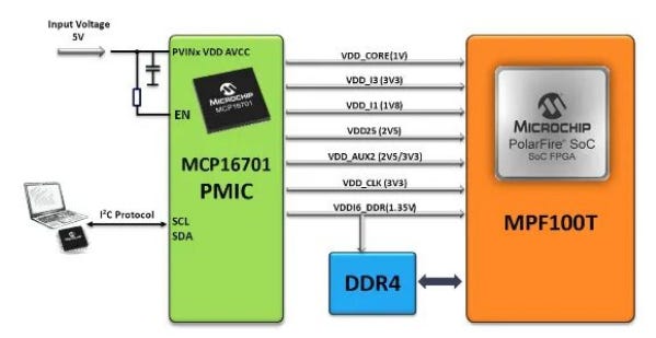
Microchip’s recently introduced MCP16701 and MP164GX1000 PMICs reflect this trend: they integrate eight parallel-capable 1.5A buck converters, four 300mA internal LDOs, and a controller for driving an external MOSFET, enabling up to a 48% board-area reduction and cutting component count to less than 60% compared with discrete solutions. These devices also support dynamic output-voltage adjustment in 12.5 mV or 25 mV steps, allowing fine-grained power tuning to improve efficiency and performance. For advanced sensors and MPU process nodes, output-voltage accuracy below ±1% across the full operating temperature range is increasingly important. Packaged in a compact 8 mm × 8 mm VQFN form factor, these PMICs show why power management is becoming a strategic design layer for future AI, industrial automation, and high-performance embedded systems: as compute density rises, the ability to deliver clean, precise, efficient, and thermally manag

8-inch Capacity: Less About Total Volume, More About Value Mix
VIS expects 2026 8-inch capacity to reach 3.306 million wafers, down 4% year-on-year. The decline is mainly due to the conversion of coarse-linewidth capacity into finer-linewidth capacity. At first glance, lower capacity may look negative. But for specialty foundries, total wafer capacity is not the only metric that matters.
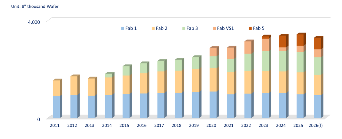
VIS operates a total of five 8-inch wafer fabs, including four in Taiwan and one in Singapore. Its annual capacity in 2026 is expected to be approximately 3.3 million 8-inch wafers.
The more important question is whether capacity is being shifted toward higher-value products.
VIS expects 2Q26 monthly capacity to increase 4% quarter-on-quarter to 277,000 8-inch wafers due to more working days and debottlenecking. Fab 5 is expected to expand to 30,000 wafers per month by the end of 2026, with another 10,000 to 20,000 wafers of cleanroom space potentially available. Singapore VS1 also has several thousand to around 10,000 wafers of expansion space.
However, the company made an important point: additional expansion will only proceed when customers provide clear capacity commitments. This indicates a more disciplined capital allocation model.
In the past, mature-node foundries often expanded capacity in response to cyclical demand, only to face utilization pressure when the cycle turned. VIS now appears more focused on capacity expansion backed by LTA, customer commitments, or customer-consigned equipment. This approach is structurally better for gross margin and return on invested capital.
In this sense, VIS’s 8-inch business is not merely recovering. It is becoming more selective.
VSMC: From a 12-inch PMIC Expansion to an AI-Relevant Specialty Process Platform
The most strategically important update is the adjustment of the VSMC production plan.

VIS and its customers have reached new agreements, and VSMC will no longer be positioned only as a 12-inch platform for PMIC, analog, and mixed-signal products. It will also include interposer production. This changes the meaning of the project.
VSMC is expected to produce 40nm to 130nm products, with technology coming from TSMC. This is critical. It means the Singapore 12-inch fab is not being built from scratch as an isolated mature-node facility. Instead, it extends TSMC-rooted mature process technology into an international manufacturing platform with a broader product mix.
Originally, VSMC was expected to reach full capacity of 55,000 wafers per month by 2029. Under the revised plan, full capacity is adjusted to 44,000 wafers per month, mainly due to higher process complexity and product mix changes. At first, this looks like a capacity downgrade. But that interpretation is too simple.
If interposer and more complex specialty processes carry higher value per unit of capacity than traditional PMIC products, then lower physical capacity does not necessarily mean lower economic value. At the same time, customer-consigned equipment and stronger capacity commitments reduce VIS’s capital burden. Expected capex falls from US$7.8 billion to US$6.7 billion.
This is the core of the revised VSMC investment case: lower capacity, but higher product value; lower capex, but stronger customer commitments; still some depreciation pressure, but a better path to earlier breakeven shipment volume.
For VIS, this is more attractive than building a conventional 12-inch PMIC fab.
Latest Progress at VSMC’s Singapore Fab: AI Customers Rush to Secure Capacity as VIS Begins to Evaluate a Second 12-inch Fab
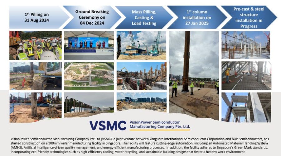
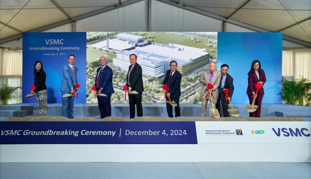
The VSMC 12-inch fab in Singapore has become one of the most closely watched indicators for Vanguard International Semiconductor’s next phase of growth amid rising AI-related demand. According to VIS Chairman Fang Leuh, the fab broke ground roughly 18 months ago, and overall construction progress remains on schedule, with some parts even running ahead of plan. Civil engineering work was completed about five months ago, and more than 200 pieces of equipment have already entered the cleanroom for large-scale installation.
Under the current plan, VSMC is expected to begin customer sample delivery in July this year, while the schedule for mass production in the first quarter of 2027 remains unchanged, with the possibility of further acceleration. VIS originally planned to complete the full capacity ramp by 2029, but based on current customer demand and fab construction progress, full loading could potentially be pulled forward to 2028.
More importantly, the capacity of the first fab has already been almost fully reserved by customers, with part of the demand supported by long-term agreements. Fang acknowledged that a number of customers are continuing to request additional capacity, which has led the company to seriously evaluate whether the second 12-inch fab, or P2, should be launched earlier than originally planned.
However, he also emphasized that VIS will maintain its historically prudent approach to capacity expansion. The foundry industry has experienced multiple cyclical reversals in the past. Once new capacity comes online, a demand downturn could dilute gross margin and overall operating performance. Therefore, the company will continue to assess long-term demand visibility and the degree of customer commitment before deciding the next step in its investment pace.
A notable development is that VSMC’s product mix is also beginning to evolve. In addition to its original focus on PMIC, mixed-signal, and analog processes, part of the fab’s capacity has now been allocated to interposer-related business.
Since the interposer is a critical component in AI advanced packaging platforms such as CoWoS, the market is interpreting this as a sign that VIS is gradually moving deeper into the higher-value segments of the AI supply chain through its Singapore fab.
Fang said that interposer demand has already been agreed upon with customers and is now underway. This should help improve capacity utilization, shorten the time to breakeven, and further support gross margin performance. However, because many of the related customers are covered by confidentiality agreements, VIS has not disclosed specific partners or shipment scale.
As for the cost structure of the Singapore fab, Fang admitted that Singapore, compared with Taiwan, is a high-cost location. Labor costs and depreciation pressure are both higher, and the heavier equipment depreciation associated with a new fab means that overall manufacturing costs will certainly be above those of VIS’s Taiwan fabs.
Nevertheless, he believes that as global geopolitical risks continue to rise, customers are no longer evaluating foundry partners based solely on unit cost. Instead, they are placing greater emphasis on overall supply chain security, service capability, and risk diversification. For many international customers, Singapore offers a certain geopolitical advantage, making the higher cost still acceptable and manageable.
On the talent front, VSMC’s first fab has already recruited around 700 employees. As capacity gradually ramps, the workforce could exceed 1,000 people between 2028 and 2029. Given the limited local pool of technical talent, the company is also recruiting globally, bringing in semiconductor professionals from Malaysia, China, and other regions.
VIS Continues to Focus on Specialty Mature Processes, While Leaving the Door Open for 22nm
Regarding process strategy, Fang once again emphasized that VIS will not chase the most advanced process-node race. Instead, the company will continue to focus on specialty mature processes and application-specific markets, including PMIC, BCD, automotive, and industrial control. He acknowledged that VIS is a relatively late entrant in the 12-inch foundry market, making it more important for the company to extend its accumulated strengths in 8-inch specialty processes rather than blindly invest in leading-edge Moore’s Law nodes.
However, when asked whether the future P2 fab could move further into more advanced processes such as 22nm, Fang left a meaningful response: “Never say never.”
LTA and Customer-Consigned Equipment Reduce VSMC Risk
The market’s main concern about VSMC has always been depreciation. A new 12-inch fab requires heavy upfront investment, and once depreciation begins, gross margin can come under pressure if utilization is not high enough.
The latest update reduces this risk in three ways.
First, the Fab 1 line is already fully booked, and all capacity is supported by LTA.
Second, customers will consign part of the equipment, lowering VIS’s own capital expenditure.
Third, because interposer production is now part of the plan, the company expects the timeline to full loading to move forward, shortening both the duration and magnitude of gross-margin pressure.
This is not a typical build-it-and-hope-the-demand-comes expansion model. It is closer to a shared-investment model backed by actual customer demand, equipment support, and long-term capacity commitments.
In other words, VIS is not bearing the entire VSMC risk alone. Part of the capital risk is being transferred to customers who genuinely need the capacity.
The company also indicated that under the revised plan, it has greater confidence in achieving the goals proposed in 2024, including full loading by 2029 and revenue doubling, with the possibility of achieving them earlier. This is one of the most positive signals from the latest update.
5月8日
Interposer Brings VIS Closer to the AI Infrastructure Supply Chain
The inclusion of interposer production is strategically meaningful because it brings VIS closer to the AI infrastructure supply chain.
Historically, VIS has been viewed mainly as a PMIC, DDIC, and mature-node foundry. Interposer changes that perception. Interposers are important elements in advanced packaging and high-performance computing systems. VIS will not become a CoWoS provider because of this, but its role moves closer to the peripheral process layer of AI packaging infrastructure.
This matters because the boundary between mature process and advanced packaging is becoming less clear. AI chips require advanced logic, but the broader package and system also require many mature-node capabilities: interposer-related processes, power management, controllers, sensors, protection devices, and mixed-signal circuits.
None of these are transistor-scaling races. But without them, AI systems cannot function reliably.
Therefore, VIS should not be described only as a mature-node foundry. More precisely, it is becoming a specialty process platform supporting AI infrastructure.
This also explains why interposer is viewed as positive for gross margin. It is not just an additional product. It is an entry point into a higher-value product mix.
5月14日
Compound Semiconductors: GaN and SiC as Long-Term Optionality
Beyond 8-inch and VSMC, VIS’s compound semiconductor roadmap also deserves attention.
The company has indicated that low-voltage GaN on QST and GaN on silicon are already in production, and both can meet data center product requirements. The latest GaN on QST product has completed qualification and started taking orders. The 650V GaN on silicon technology transferred from TSMC is currently in transition and is expected to enter mass production in 2H27.
For SiC, VIS currently has a pilot line and expects mass production by the end of 2026, with IDM customers as the first wave.
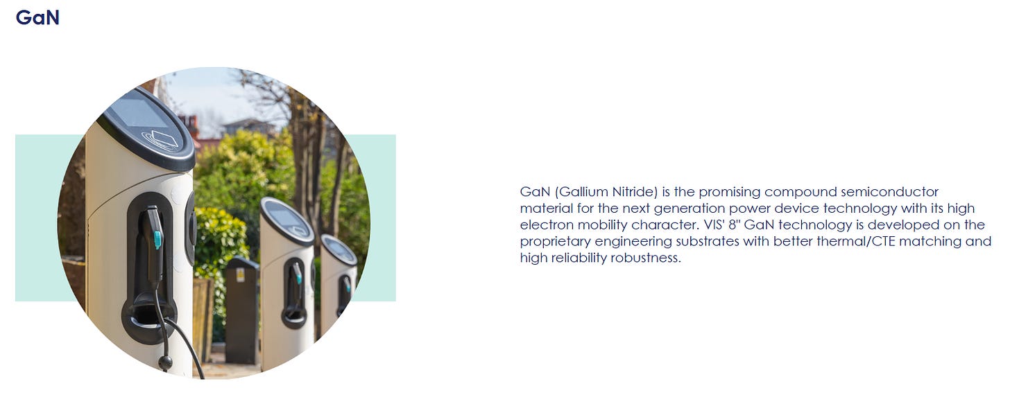
These businesses may not contribute significantly to near-term revenue, but they represent important medium- to long-term optionality. As AI data center power consumption increases, power conversion efficiency becomes increasingly important. Future demand will not only come from PMIC on server boards. It will also come from power supplies, rack-level power delivery, voltage conversion, cooling systems, and high-efficiency power devices.
If VIS can establish stable manufacturing capability in GaN and SiC, it may extend from traditional PMIC foundry services into higher-power-density compound semiconductor applications.
This could become an important growth layer in the next stage of AI infrastructure buildout.

The device's outstanding figure of merit (FOM) surpasses silicon-based transistor under high switching frequency that makes the GaN becomes the optimum solutions for high power efficiency products in high performance computing and electrical vehicle applications.
Equipment Transfer and the Logic of Capital Efficiency
The TSMC-VIS relationship is also visible in equipment transfer and mature-node capacity redeployment.
As TSMC increasingly concentrates resources on advanced logic and advanced packaging, some older 6-inch and 8-inch assets become less strategic inside TSMC’s own capital allocation system. These assets may still have industrial value, but they no longer represent the highest-return use of TSMC’s cleanroom space, engineering bandwidth, and management attention.
For VIS, however, these assets can be highly useful. Acquiring mature-process equipment from TSMC allows VIS to expand capacity at lower cost, support customer demand, and preserve continuity for mature-node products.
The key is not simply equipment purchase. The key is process continuity.
Mature-node customers are highly sensitive to requalification. Moving a product from one foundry to another can require validation of process parameters, yield behavior, reliability, packaging compatibility, and end-customer certification. This takes time and money. If the switching cost is too high, customers prefer to stay with the original supply chain.
Because VIS shares technology lineage and equipment familiarity with TSMC, it can become a relatively smoother landing point for mature-node orders that TSMC no longer wants to prioritize. This is the so-called “painless transfer” logic.
For TSMC, it is asset optimization. For VIS, it is low-cost capacity expansion. For customers, it is supply chain continuity.
This is capital efficiency at the ecosystem level.
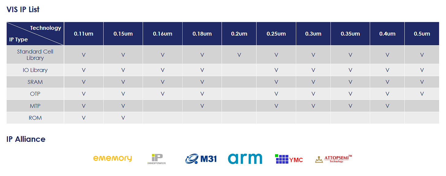
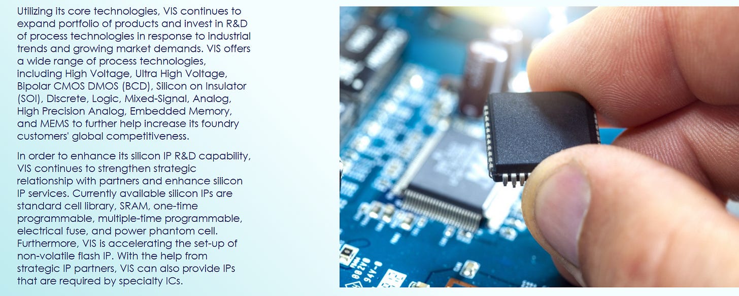
VIS provides the best-in-class foundation IPs (Std. Cell Library, GPIO, and Memory) that are optimized to VIS technology platforms with silicon-proven record to support customer's design and on-time production. The table below presents the released libraries and qualified IPs from VIS and the alliance of the 3rd-party IP vendors.
Taiwan’s Semiconductor Strength Is Not Just One Company, but Layered Specialization
The broader strategic lesson is that Taiwan’s semiconductor strength does not come only from TSMC’s leading-edge dominance. It also comes from layered specialization.
TSMC pushes the frontier of compute performance. VIS supports the mature and specialty process base. ASE, SPIL, and other OSATs support packaging and test. Substrate, PCB, materials, equipment, and component suppliers form the surrounding manufacturing network. This layered structure is why Taiwan’s semiconductor ecosystem has resilience.

In the AI era, this structure becomes even more important.
AI infrastructure is not a single chip story. It is a system architecture story. A GPU needs HBM. HBM needs advanced packaging. Advanced packaging needs interposers, substrates, thermal materials, bonding processes, and test capacity. The server board needs PMIC, power stages, controllers, retimers, sensors, and protection devices. The data center needs power conversion, cooling, optics, networking, and system-level integration.
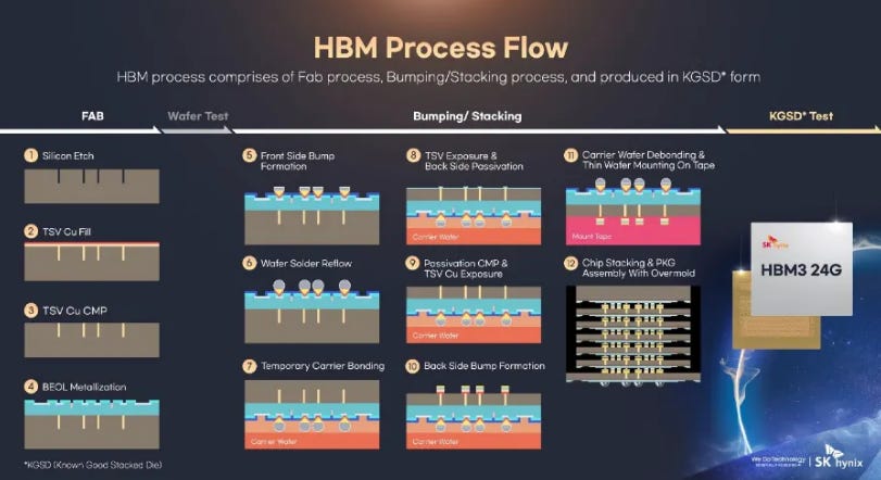
Therefore, mature process is not old technology in the negative sense. It is foundational technology.
When AI clusters become larger, power-hungrier, and more complex, the value of reliable mature-node supply increases. This is where VIS becomes strategically more relevant than before.

5月18日
Conclusion: VIS Is Entering a Mature-Node Structural Improvement Cycle
VIS’s latest message is clear: mature-node supply and demand are entering a structurally better phase. Consumer electronics remain uneven, and PC and smartphone demand are still affected by capacity allocation and end-market uncertainty. But AI demand is strong across both advanced and mature processes, supporting VIS’s visibility into 2H26.
In the short term, VIS is benefiting from a synchronized improvement in shipments, ASP, utilization, and gross margin. The expected rise of utilization to 85–90% from 2Q26 onward is the key driver of 8-inch profitability recovery.
In the medium term, the revised VSMC plan reduces the risk profile of the Singapore 12-inch project. Interposer production, 100% LTA coverage for Fab 1, customer-consigned equipment, and lower capex all improve the probability that the project reaches breakeven shipment volume earlier than previously expected.
In the long term, GaN, SiC, and 12-inch specialty processes provide VIS with optionality in high-efficiency power, data center infrastructure, automotive, and industrial applications.
The most important change is not simply that the cycle is recovering. The real change is that the market is beginning to understand the value of mature processes differently.
AI does not only drive advanced nodes. AI also requires mature nodes for power delivery, control, sensing, protection, display, and reliability. As AI systems become larger and more power-intensive, mature and specialty processes are no longer just low-growth legacy technologies. They are part of the foundation of next-generation computing infrastructure.
VIS’s story is therefore changing. It is no longer just an 8-inch PMIC and DDIC foundry. It is becoming a key node in the AI infrastructure supply chain, positioned at the intersection of mature process, specialty process, interposer-related manufacturing, power management, and compound semiconductors.
TSMC determines how high Taiwan’s semiconductor industry can go. VIS helps determine how deep and resilient the industry foundation can become.
That is why VIS deserves to be re-understood: not as TSMC’s subsidiary, not as a smaller TSMC, but as a non-subsidiary ally in the mature-node layer of Taiwan’s semiconductor strategy.

Thanks for reading SEMIVISION @_@! This post is public so feel free to share it.
TSMC recently announced two major divestment plans related to its subsidiary, Vanguard International Semiconductor (VIS):
First, in May 2026, VIS announced that it would sell up to 152 million ordinary shares of Vanguard International Semiconductor Singapore through block trades to financial institutional investors, equivalent to approximately 8.1% of VIS’s stake. After the transaction, VIS’s shareholding in the Singapore subsidiary will decline from 27.1% to around 19%. The company emphasized that there are currently no further plans to sell additional shares and that this move is mainly intended to optimize capital allocation and focus resources on its core business. It will not affect existing strategic cooperation, including foundry outsourcing and gallium nitride technology licensing.
Second, in May 2025, VIS’s board approved the disposal of a batch of unused machinery and equipment to its Singapore subsidiary, VSMC, with a total transaction value of approximately US$71–73 million, or around NT$2.2 billion. This transaction was mainly aimed at improving asset utilization and supporting the development of the Singapore subsidiary.

5月5日


PreviousNext