From Electrons to Photons: CPO Test Interfaces Become the Next AI Infrastructure Battleground
From Electrons to Photons: CPO Test Interfaces Become the Next AI Infrastructure Battleground
- Source: SemiVision
- Author: SEMIVISION
- Published: 2026-05-25T21:26:52+08:00
- URL: https://tspasemiconductor.substack.com/p/from-electrons-to-photons-cpo-test (1) From Electrons to Photons: CPO Test Interfaces Become the Next AI Infrastructure Battleground


From Electrons to Photons: CPO Test Interfaces Become the Next AI Infrastructure Battleground
Original Article By SemiVision Research [Reading time: 20 mins]

May 25, 2026
∙ Paid
From Electrons to Photons: CPO Test Interfaces Become the Next AI Infrastructure Battleground

CPO (Co-Packaged Optics) is heating up fast and becoming one of the hottest topics in the semiconductor and AI industry right now.
Driven by the explosive demand for massive bandwidth and ultra-low power in next-generation AI factories, SiPh/CPO has emerged as the critical enabling technology for both today’s scale-out networking and tomorrow’s scale-up xPU fabrics. Major players are moving quickly: Intel is pushing Optical Compute Interconnect (OCI), NVIDIA has unveiled its Quantum-X and Spectrum-X Photonics platforms, TSMC, GlobalFoundries, Broadcom, Marvell, and Ayar Labs are all rolling out new products and manufacturing platforms. The market momentum is unmistakable — CPO is no longer just a promising concept, but a rapidly commercializing solution that the entire industry is racing to adopt.
The Critical Shift from Electrons to Photons: How CPO Test Interfaces Are Becoming a New Battleground for AI Infrastructure
AI infrastructure is entering a critical inflection point. In the past, when the semiconductor industry discussed computing power, the focus was mostly on GPUs, ASICs, HBM, advanced process nodes, and advanced packaging. Today, however, the real bottleneck limiting system performance is gradually shifting from “whether chips can compute” to “whether data can move efficiently.”
This is why CPO, or Co-Packaged Optics, has become one of the most closely watched technologies in the industry. CPO is not merely about making optical modules smaller, nor is it simply about increasing transmission speed by one generation. More importantly, it represents a new stage in AI system architecture, where traditional electrical interconnects are gradually moving toward deeper optoelectronic integration.
From WinWay’s CPO technology forum, it is clear that the challenges of CPO do not lie only in optical engines, silicon photonics chips, or packaging integration. They also lie in mass-production testing. When optics, electrical signals, thermal management, mechanical alignment, and high-speed signaling all converge within the same package, the test interface is no longer just a supporting role in the semiconductor manufacturing process. It becomes a critical factor determining whether CPO can truly move into commercial deployment and volume production.
5月14日
The Real Bottleneck in the AI Era Is Not Only Computing Power, but Data Movement
The core challenge of AI servers is shifting from single-chip performance competition to system-level competition in bandwidth, latency, and power consumption.
In large model training and inference, GPUs or ASICs do not operate in isolation. They must continuously exchange massive amounts of data with HBM, switches, NICs, optical modules, and the broader data center network. As model size, parameter count, and token traffic continue to grow, data movement itself becomes a major cost.
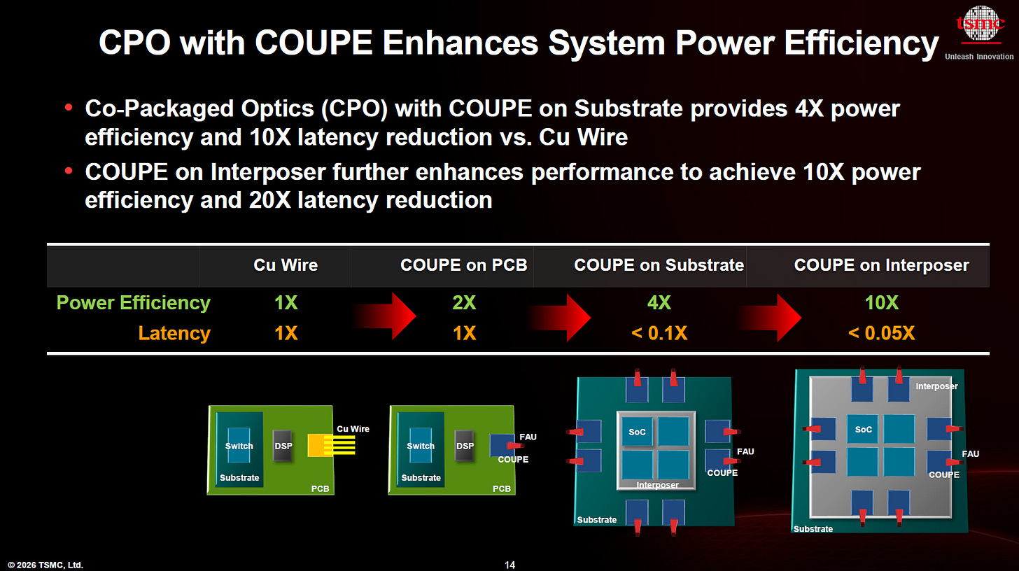
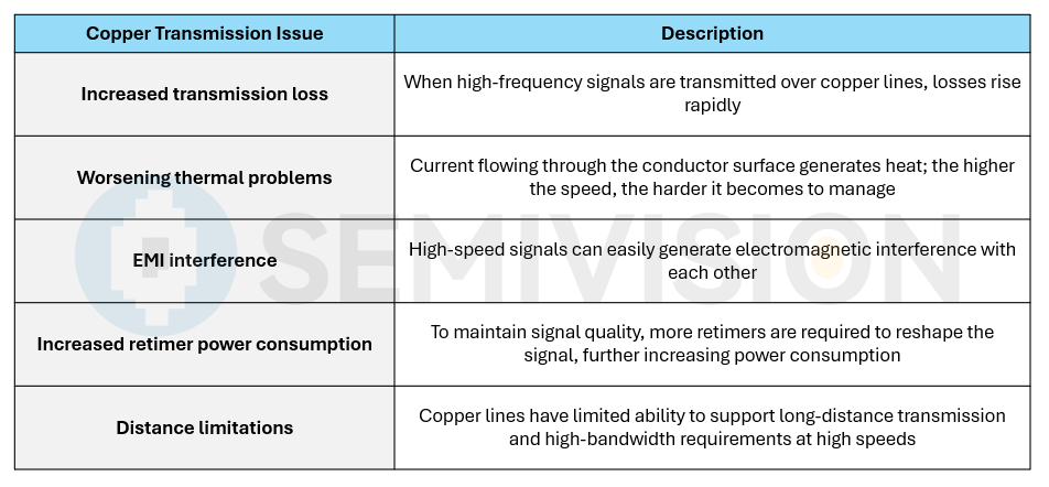
Traditional copper wires or PCB traces face clear limitations under high-speed transmission. When signal speeds move into the 112 Gbps, 224 Gbps, and eventually 448 Gbps range, electrical signals transmitted through copper face three major challenges: higher loss, higher power consumption, and shorter transmission distance.

2025年7月8日
This is not a problem that can be fully solved simply by switching to better materials. It is a sign that physical limits are approaching. High-speed electrical signals in copper are affected by skin effect, dielectric loss, reflection, crosstalk, and package parasitics. The higher the speed, the shorter the viable transmission path, the tighter the design tolerance, and the higher the overall system cost.
Therefore, what AI infrastructure needs is not only faster chips, but also more efficient data channels. This is where optical communication creates value. Optical signals offer low loss, long-distance transmission, high bandwidth, and immunity to electromagnetic interference. They can redefine how chips, switches, and networks are connected inside the data center.
Below we will share:
The Core Meaning of CPO: Bringing Optical Engines Closer to Computing Chips
The Hardest Part of CPO Is That It Pushes Testing to the Physical Limit
WinWay’s Role: From Electrical Test Interfaces to CPO Optoelectronic Integration Test Platforms
Thermal Management Is Becoming a Core Battleground for Test Interfaces
Before CPO Reaches Volume Production, CPC May Serve as a Transitional Solution
Glass Substrates and Standardization Will Determine the Speed of CPO Scaling
AI Chip Shipments Drive Demand for Testers
Global Semiconductor Test Consumables Vendors Are Entering a Volume-and-Value Growth Cycle

2025年8月20日
The Core Meaning of CPO: Bringing Optical Engines Closer to Computing Chips
However, as AI clusters scale rapidly, pluggable optics are also beginning to encounter bottlenecks. The issue is not only the optical module itself. The more important problem is that there is still a high-speed electrical signal path between the chip and the optical module. The longer this distance becomes, the higher the power consumption and the more difficult the signal integrity challenge.

The basic logic of CPO is to place the optical engine directly beside the switch chip, ASIC, or advanced package. This allows the electrical signal to travel only a very short distance before being converted into an optical signal for external transmission.
In other words, CPO is not simply about shrinking the optical module. It is about moving the location of optical-electrical conversion from the edge of the system board to the side of the chip. This change will reshape the architecture of AI servers and data center networks.
CPO brings three important benefits.
First, it shortens the high-speed electrical signal path, reducing loss and power consumption.
Second, it increases bandwidth density inside and outside the package, enabling more data to be transmitted within limited space.
Third, it brings optics and advanced packaging into deeper integration, meaning that future AI systems will no longer be only a chip design problem, but a system engineering problem involving electrical, optical, thermal, mechanical, and material co-optimization.
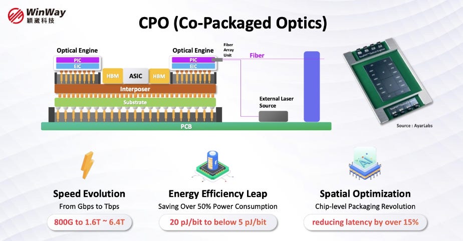
This is why CPO is viewed as an important direction for the next stage of AI infrastructure. As 800G, 1.6T, and even higher-speed interconnects become standard, optics will no longer be limited to transmission between data center racks. Light will gradually move closer to the chip and may even become part of the internal packaging architecture.
The Hardest Part of CPO Is That It Pushes Testing to the Physical Limit
The theory behind CPO is clear, but mass production is extremely difficult. One of the biggest challenges is testing.

Traditional semiconductor testing mainly deals with electrical signals. The core task of test sockets, probe cards, and test carriers is to enable test equipment to make stable contact with chips or packages for electrical measurement. CPO is different. It requires both electrical testing and optical testing, and the precision requirement for optical alignment is extremely high.
The core diameter of the single-mode fiber used in CPO is only about 9 micrometers. This means that during testing, the fiber, optical engine, coupler, and optical waveguide on the chip must be aligned with extreme precision. Even a displacement of a few micrometers can significantly reduce optical coupling efficiency and distort the test result.
This creates a major challenge for mass-production testing. Semiconductor testing is not a laboratory demonstration. It must perform repeated, stable, and measurable testing on large volumes of wafers, chips, packages, or modules within limited time. If every fiber requires long active alignment, test time and cost will rise quickly, directly affecting the commercialization speed of CPO.
Therefore, the core challenge of CPO testing is not “whether it can be tested,” but “whether it can be tested stably under mass-production conditions.” This is exactly where test interface companies such as WinWay create value.

2025年8月10日
WinWay’s Role: From Electrical Test Interfaces to CPO Optoelectronic Integration Test Platforms
According to WinWay’s CPO technology forum, the company has proposed a comprehensive CPO testing solution. As leading silicon photonics companies define higher specifications for CPO transmission, including 400G bandwidth and high-speed signaling at 224 Gbps / 448 Gbps, CPO testing is no longer just an extension of traditional electrical testing. It is entering a new stage of joint validation across optics, electronics, thermal management, mechanics, and packaging.
At the Wafer / Chip Level, WinWay provides WLCSP wafer-level probe cards for wafer-level and chip-level testing. At the Wafer Level, this solution can support an “electrical input from the top, optical output from the bottom” testing architecture, where electrical contact is made from above and optical signal measurement is performed from below. This design is highly important for CPO and silicon photonics testing because it allows optical-electrical conversion capability to be verified at the wafer stage, rather than waiting until packaging or module assembly is completed before discovering potential issues.
At the Chip Level, WinWay provides an “optical input from the top, electrical output from the bottom” solution, allowing the test system to be flexibly configured according to different chip architectures, optical engine layouts, and signal paths. This shows that CPO testing is no longer a one-directional or single-interface contact problem. It must simultaneously handle optical paths, electrical paths, mechanical compression, and thermal paths in three-dimensional space.
At the Package Level, the challenge becomes even more difficult. In a CPO package, the optical engine, switch chip, substrate, fiber array, and high-speed electrical interface must be highly integrated. The test system must also be able to handle signals from both the top and bottom sides of the package. To address this, WinWay has introduced its proprietary micro-pitch alignment double-sided probing system total solution, specifically designed for CPO testing at the Package Level. The key value of this double-sided probing system is not merely that it can test from both sides, but that it can balance micron-level optical alignment, high-speed electrical contact, and package warpage control.
At the Module Level, CPO testing becomes closer to the real system environment. The test object is no longer just a single chip or package, but a complete system that includes the optical engine, electrical connection, thermal structure, and module-level signal integrity. WinWay’s cross-generation HyperSocket™ test socket is a key solution designed for Module Level testing requirements. Facing large AI packages, high pin counts, high power consumption, and high current density, HyperSocket™ can further improve contact stability, load-bearing capability, and test reliability.
From this perspective, WinWay’s CPO strategy is not simply about launching a single test product. It is about building a complete test path from wafer, chip, and package to module. This is exactly the capability CPO needs as it moves toward mass production: not a single-point breakthrough, but the ability to validate, screen, and industrialize the entire optoelectronic packaging system at every stage of manufacturing.
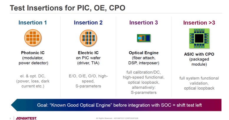
This shows that CPO testing is no longer a single-interface problem. It has become a three-dimensional integration problem. The test system must simultaneously consider the top side, bottom side, side access, optical path, electrical path, thermal path, and mechanical compression structure. In the future, the competitiveness of test interface suppliers will extend beyond contact materials and processing precision to full system integration capability.

2025年7月16日
AI chip packages are becoming larger, I/O counts are increasing, and power consumption is rising. When package size exceeds 100 mm and the number of contact points reaches tens of thousands or more, traditional test sockets face multiple challenges, including contact stability, pressure distribution, warpage compensation, and high-current carrying capability.
WinWay’s HyperSocket is designed precisely for this type of advanced AI and CPO package testing demand.
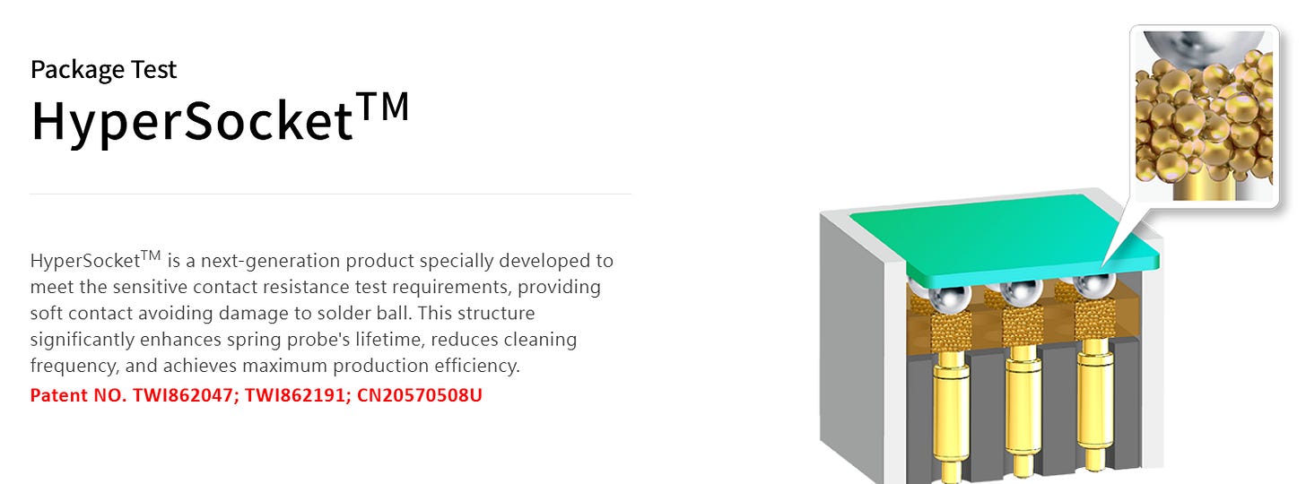
Its core concept is to combine the advantages of carbon pins and conductive elastomer. Carbon pins provide sufficient travel to compensate for package flatness variation and warpage, while conductive elastomer provides surface contact, enabling more uniform current distribution and reducing localized contact pressure and contact resistance.

This is especially important for advanced packaging. AI chip packages are not only becoming larger in area; they may also experience warpage due to material stacking, coefficient of thermal expansion mismatch, and process-induced stress. If the test interface cannot maintain uniform contact, it may cause false failures, poor contact, solder ball damage, and even affect yield analysis.
Therefore, the significance of HyperSocket is not merely an improvement in test socket design. It is a response to the structural needs created by the scaling of AI packaging. As CPO, CoWoS, SoIC, 2.5D / 3D IC, and future glass substrates continue to evolve, test interfaces must also move toward higher precision, higher reliability, and higher load-bearing capability.
Thermal Management Is Becoming a Core Battleground for Test Interfaces
Another critical challenge in CPO testing is heat.
AI chip power consumption is rising rapidly. High-end GPUs, ASICs, and switch chips generate enormous heat during testing. If this heat cannot be removed immediately, test results may become unstable, chips may throttle, and the test socket itself may suffer thermal damage.
In the past, cooling was mostly viewed as a system-level or server-level issue. But in AI chip testing, thermal management has already moved into the test interface. Testing is not a low-power scenario. In many cases, it must simulate the real operating condition of the chip under high load. This means the test socket itself must have stronger cooling capability.
WinWay has proposed introducing non-conductive engineering liquid into the test socket and using liquid cooling to remove heat. This reflects an important trend: future test interfaces will not merely be signal contact tools. They must also serve as platforms for electrical connection, mechanical support, thermal management, and optical alignment.
As AI chip power consumption continues to rise, liquid-cooled testing may no longer be a niche solution for extreme cases. It could become a necessary requirement for advanced AI package testing.

Before CPO Reaches Volume Production, CPC May Serve as a Transitional Solution
It is also worth noting that before CPO becomes fully mature, the market has begun discussing CPC, or Co-Packaged Copper, as a transitional solution.
This shows that AI interconnect technology will not follow a single path. In the future, multiple solutions may coexist, including pluggable optics, LPO, CPO, CPC, AEC, and ACC. Each will be selected based on distance, power consumption, cost, serviceability, and system architecture.
From SemiVision’s perspective, CPO remains the long-term direction, but CPC reflects the industry’s pragmatic strategy in the short to medium term. Customers will not simply pursue the most advanced technology. They will choose the solution that best matches system cost, reliability, and deployment timing.

3月6日
Glass Substrates and Standardization Will Determine the Speed of CPO Scaling
For CPO to truly enter large-scale production, two key conditions are still required: new material platforms and standardization.
The first is the glass substrate. Glass has a low coefficient of thermal expansion, high dimensional stability, and excellent flatness, making it an important candidate material for next-generation advanced packaging. In CPO architecture, glass substrates may even integrate optical waveguides, allowing optical signals to travel inside the substrate and further increasing optoelectronic integration density.
This means that future package substrates will not only carry electrical signals. They may also become part of the optical signal path. Once the substrate evolves from a circuit carrier into an optoelectronic hybrid platform, materials, processing, alignment, testing, and reliability will all be reshaped.
The second is standardization. If every company uses different optical engines, package interfaces, fiber arrangements, and test specifications, the cost of CPO mass production will be extremely high. Only when switch chips, optical engines, package interfaces, and test specifications gradually become standardized can CPO move from customized engineering to scalable industrialization.

This is also why leading companies such as NVIDIA are pushing CPO switch specifications. Standardization does not restrict innovation. Instead, it allows the supply chain to invest collaboratively and enables optical engines, test interfaces, packaging materials, and system vendors to form a reproducible mass-production architecture.

Conclusion: The Success of CPO Depends Not Only on Optics, but on the Test Interface
CPO is viewed as an important technology for the AI era not because it sounds advanced, but because AI infrastructure is approaching the limit of electrical interconnects. When data movement becomes the system bottleneck, optics must move closer to the chip.
But CPO cannot succeed through optical engines or silicon photonics chips alone. The real difficulty lies in integrating optics, electronics, thermal management, mechanics, and packaging into a system that can be mass-produced, tested, serviced, and accepted by data center customers.
Future CPO competition will not only be about who can build a faster optical engine. It will also be about who can turn optical packaging into a manufacturable, verifiable, and scalable industrial platform. For Taiwan, this represents a new opportunity. Beyond foundry manufacturing and advanced packaging, test interfaces, materials, substrates, optical alignment, and thermal management will all become new value coordinates in the semiconductor supply chain of the AI era.
AI Chip Shipments Drive Demand for Testers
The continued growth in AI chip shipments, combined with increasingly complex designs, is rapidly driving up demand for semiconductor testing. According to the latest industry report, global data center AI chip shipments are expected to increase from 23.8 million units in 2024 to 53.4 million units by 2030.
This data center AI chip category includes high-end and mid-range GPUs, dedicated AI chips such as Google’s TPU, AI server CPUs, and networking/interconnect-related chips, including switch ASICs, rack-level interconnect chips, DPUs, and NICs.
In general, as transistor counts increase, testing complexity grows almost exponentially, as chips require more test patterns and longer test times. Testing protocols must cover high-speed interconnects, stress conditions, thermal conditions, and multiple operating modes.
AI chips are highly complex in design, and the stacked architecture used in CoWoS advanced packaging further extends overall testing time. Wafer-level testing time for AI chips is expected to increase by more than 50% compared with conventional chips, while final test time may be extended by two to three times. Longer test times are likely to push existing testing capacity toward full utilization, thereby driving demand for additional test equipment purchases.
Innovation in semiconductor technology, including advances in high-performance computing (HPC), nanoscale silicon process nodes, and silicon photonics, is requiring automatic test equipment (ATE) to evolve at an unprecedented pace.
As chip complexity continues to increase, the challenges involved in design, manufacturing, and testing are also multiplying. To achieve the performance gains required for high-performance computing and edge computing, the industry continues to push process scaling forward, with chip process nodes now entering the angstrom era.

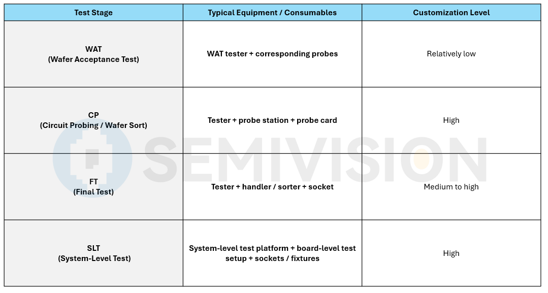
Test Consumables Are Expected to See Continued Growth in Both Volume and Value
Test consumables are also expected to benefit from rising demand and higher average selling prices. As semiconductor process technology advances toward 2 nm and below, and as advanced packaging technologies such as chiplets and 3D stacking enter large-scale adoption, chip pin counts, test density, and signal complexity are increasing exponentially. This is driving probe cards to evolve toward higher density, higher frequency, greater current-carrying capability, and better thermal dissipation performance.
Taking high-end probe cards for AI chip testing as an example, pin counts have already increased from the traditional level of several hundred pins to thousands or even tens of thousands. Over the next few years, the number of pins on a single probe card is expected to move toward 400,000 to 500,000. Rising technical barriers are making MEMS probe cards the mainstream solution in the high-end market, directly increasing product unit prices and added value.
At the same time, AI servers, GPUs, HBM, and related chips not only require longer test cycles, but also feature high power consumption and large package sizes. These characteristics impose stringent requirements on the thermal stability and signal integrity of test interfaces, further driving market demand for high-end probe cards as well as supporting test load boards and test sockets.
Global Semiconductor Test Consumables Vendors Are Entering a Volume-and-Value Growth Cycle

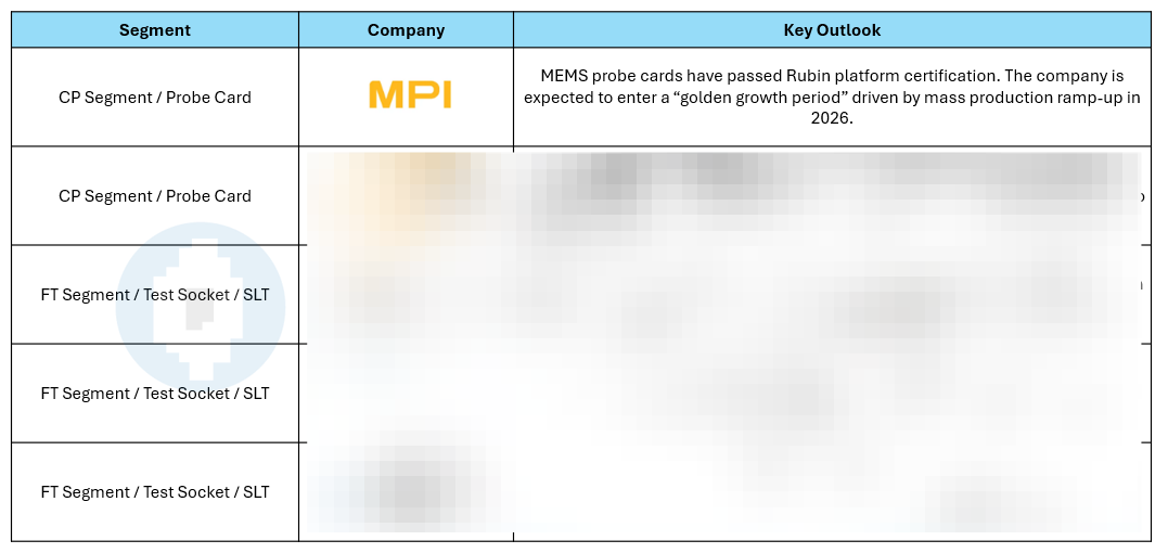
In the CP, or chip probing, segment, MPI Corporation is one of Taiwan’s key probe card suppliers, offering a broad portfolio that includes fine-pitch cantilever probe cards, high-speed vertical probe cards, and MEMS-based solutions. MPI also provides an integrated probe card solution covering probe heads, substrates, and PCBs, positioning the company as a full-solution provider for wafer-level testing. Its MEMS probe cards have reportedly passed Rubin platform certification, which could support both volume growth and ASP expansion as AI/HPC platforms move toward mass production.

MJC, or Micronics Japan Co., Ltd., remains a major global probe card supplier with strong exposure to memory testing. The company has been expanding production capacity for memory-related applications, including through its Aomori facilities, as HBM demand continues to rise. As next-generation HBM becomes increasingly important for AI accelerators, MJC’s technology roadmap and memory customer base position it to benefit from the structural expansion of DRAM and HBM testing demand.

In the FT, or final test, segment, WinWay Technology is benefiting from rising demand for AI chip test interfaces. The company has stated that it plans to double its probe capacity in 2026 to support strong demand from AI applications and servers. WinWay is also expanding its global footprint, including plans for an Arizona facility, as customers increasingly require localized and geopolitically diversified test interface capacity.
Smiths Interconnect is leveraging its DaVinci Gen V platform to provide ready-to-use test interface solutions for advanced ASICs. For leading-edge AI ASICs, where development cycles are compressed and yield learning is critical, turnkey test interface solutions can help customers shorten qualification time, reduce engineering complexity, and accelerate volume ramp-up.
Cohu is also accelerating its exposure to the AI data center market. The company reported third-quarter 2025 net sales of US$126.2 million and highlighted demand from Neon HBM inspection and Eclipse test-handler solutions. Its Neon platform is used for inspection and metrology of HBM devices, while the Eclipse handler with active thermal control is positioned for high-power AI processors, where thermal stability during test is becoming increasingly critical.
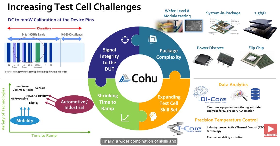
Overall, 2026 could mark a “golden growth period” for the semiconductor test consumables industry. AI compute demand, HBM scaling, advanced packaging adoption, and process-node migration are all increasing test complexity, test time, pin count, thermal requirements, and signal-integrity challenges. These factors should drive both shipment growth and ASP expansion across high-end probe cards, test sockets, load boards, and advanced test handlers.
Market Risk Factors Analysis
Risk of lower-than-expected capital expenditure by major customers
If capital expenditure by global cloud service providers, AI leaders, and major semiconductor manufacturers falls short of market expectations, or if the pace of spending growth slows, the semiconductor test consumables industry could face downside pressure. This may be caused by slower-than-expected commercialization of AI applications, weak recovery in consumer electronics, or a high-interest-rate environment that increases corporate financing costs.
Under such circumstances, upstream test consumables such as test sockets and probe cards may face reduced order volumes and lower capacity utilization. This would directly pressure the revenue and profitability of companies in the sector and could force the overall industry growth trajectory to slow.
Risk of intensifying technology competition
Competition among global technology leaders in AI chips, compute infrastructure, and other strategic semiconductor fields is becoming increasingly intense. On the technology side, faster iteration of chip architectures and process nodes is raising the performance and process-compatibility requirements for semiconductor test consumables. Companies in the industry must continue increasing R&D investment to support advanced nodes, high-end packaging, high-pin-count devices, and high-power testing requirements.
This creates the risk of rising R&D costs and potential technology lag for companies that fail to keep pace with next-generation testing demands. On the market side, price competition and local substitution trends are also becoming more visible. As companies compete more aggressively for market share, gross margins may face continued pressure, which could affect the stability of overall profitability.
Geopolitical risk
Geopolitical disruption caused by great-power competition, trade friction, export controls, and regional policy barriers could have a significant impact on the semiconductor test consumables industry, which is deeply embedded in global supply chains. Various geopolitical restrictions may limit companies’ access to critical components, increase cross-border logistics and trade costs, and create additional barriers to regional market entry. These factors could constrain overseas expansion, weaken supply chain stability, and introduce greater uncertainty into the global operating strategies of companies in the sector.
Thanks for reading SEMIVISION @_@! This post is public so feel free to share it.


PreviousNext