When HBM Becomes “Luxury Real Estate for Compute” How to Rebuild AI Memory Architecture
When HBM Becomes “Luxury Real Estate for Compute” How to Rebuild AI Memory Architecture
- Source: SemiVision
- Author: SEMIVISION
- Published: 2026-05-18T09:13:49+08:00
- URL: https://tspasemiconductor.substack.com/p/when-hbm-becomes-luxury-real-estate (1) When HBM Becomes “Luxury Real Estate for Compute” How to Rebuild AI Memory Architecture


When HBM Becomes “Luxury Real Estate for Compute” How to Rebuild AI Memory Architecture
Original Article By SemiVision Research [Reading time: 13 mins]

May 18, 2026
∙ Paid

When HBM Becomes “Luxury Real Estate for Compute” How to Rebuild AI Memory Architecture
In today’s AI compute race, the spotlight seems fixed on GPUs vs. TPUs, model size, and inference speed — an arms race measured in TOPS, parameters, and latency. But if we zoom out, the real choke point in the industry is not algorithms or silicon design.
It is the physics and supply chain structure of memory.
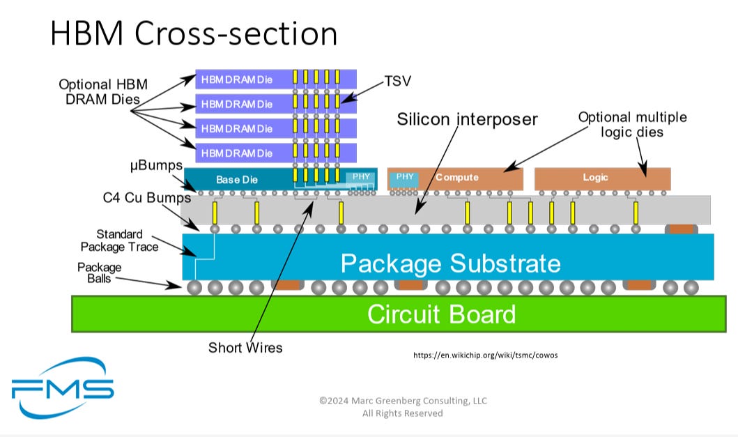
Driven by the success of NVIDIA’s system-level architecture, HBM (High Bandwidth Memory) has effectively become thedefault memory configurationfor high-end AI accelerators. In today’s AI infrastructure, memory is no longer a secondary component — it is a performance-defining element.
You can think of HBM as the most premium real estate in a megacity. The location is unbeatable: it sits extremely close to the compute die, connected through an interposer with thousands of ultra-wide data paths. The infrastructure is top-tier: 3D die stacking, TSV vertical interconnects, and advanced packaging technologies such as CoWoS enable unprecedented bandwidth density.
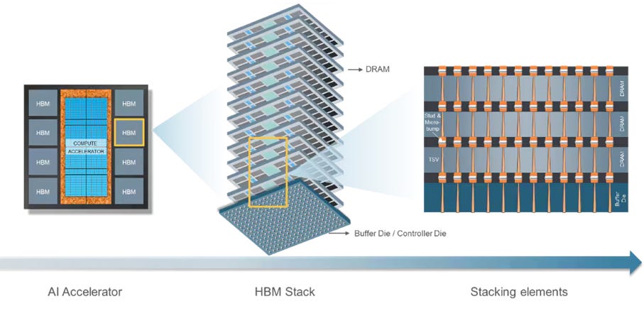
Source: AMAT
But premium real estate comes with structural consequences.
Prices are astronomical because manufacturing HBM is not just a matter of producing DRAM wafers. It involves:
High-yield TSV formation
Wafer thinning and precise stacking
Thermal management for multi-die stacks
Interposer-based advanced packaging
CXL (Compute Express Link): Making Memory Coherent
Whether vendors want to sell, how much capacity they allocate, and to whom — is not entirely in the hands of the AI chip designer.
This dynamic transforms memory from a technical specification into a strategic dependency.
Below we will share:
Why HBM Turned Into a Strategic Bottleneck
The Core Idea: Decoupling Memory from the Compute Die
Why “Closer is Better” Is Breaking Down
Google’s Architectural Reframe
OCS (Optical Circuit Switching): Memory on Demand

Not All DRAMs Are the Same
While HBM dominates AI/HPC discussions, it represents only one branch in the broader DRAM ecosystem. Different application domains drive fundamentally different DRAM architectures, interfaces, and packaging choices.
Despite their differences, these DRAM types still share a common foundation: most rely on the 1T1C (one-transistor, one-capacitor) cell to store data. The divergence happens at the system interface and packaging level, where physical constraints, power budgets, and bandwidth requirements drive different engineering trade-offs.

HBM represents the extreme end of this spectrum — optimized for bandwidth per square millimeter rather than raw capacity per dollar.
As AI models scale toward trillions of parameters, memory architecture becomes as critical as compute architecture. The question is no longer justhow fast a chipcan compute, but how effectively it can be fed with data.
HBM solved the bandwidth problem, but in doing so it concentrated power in a narrow part of the supply chain. That concentration is now pushing hyperscalers and chip designers to explore alternative memory-system architectures — not necessarily to replace HBM outright, but to regain architectural flexibility and reduce single-point dependencies.
In this sense, memory is evolving from a component choice into a strategic infrastructure decision.
This dynamic became increasingly pronounced between 2023 and 2026. AI chip companies are no longer just “technology buyers.” They have, in many ways, become hostages of the memory supply chain.
CNBC: AI memory is sold out, causing an unprecedented surge in prices
Why HBM Turned Into a Strategic Bottleneck
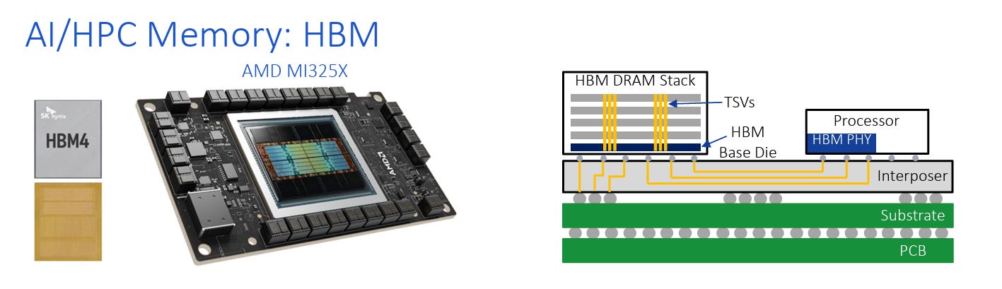
HBM’s dominance is not accidental. Technically, it achieves extreme performance through three core elements:
3D stacking– multiple DRAM dies vertically stacked to shorten internal data paths
TSVs (Through-Silicon Vias)– vertical electrical interconnects drilled through silicon
Ultra-close integration with logic dies(via advanced packaging such as interposers)

This combination enables memory bandwidth measured in terabytes per second, which is critical for large-scale AI model training. But the trade-offs are structural:
TSV fabrication is complex, yield-sensitive, and expensive
Thermal management worsens as stacks grow taller
Capacity expansion is slow due to process bottlenecks
Supply is concentrated among very few manufacturers
HBM is an architecture optimized for peak performance, not for scalable infrastructure elasticity.
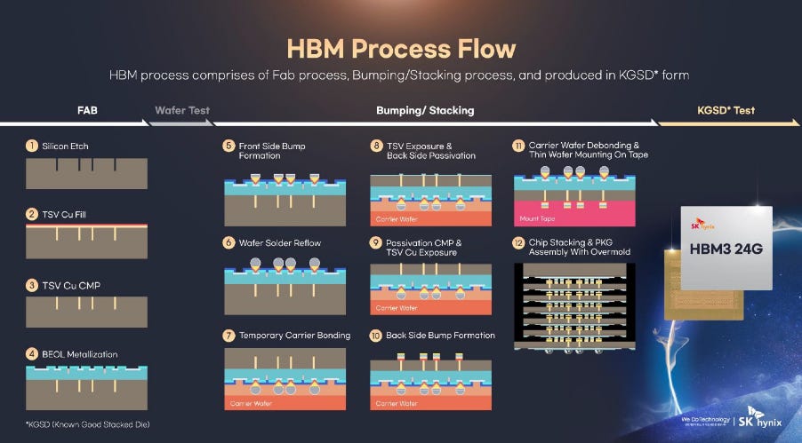
The production of HBM combines advanced wafer fabrication, 3D stacking technology, and high-end packaging engineering, making it significantly more complex than conventional DRAM manufacturing. The overall process can be divided into three main stages: front-end wafer fabrication (Fab) → bumping and stacking → final testing (KGSD Test).
During the Fab stage, memory circuits are first fabricated on the silicon wafer. This includes TSV (Through-Silicon Via) processes such as silicon etching to form vertical holes, copper filling of the TSVs, and chemical mechanical polishing (TSV CMP) to ensure planar surfaces and reliable vertical electrical connections. BEOL (Back-End-of-Line) metallization is then completed to form the signal and power interconnect network of the DRAM devices.
In the Bumping and Stacking stage, micro-bumps are first formed on the front side of the wafer, followed by solder reflow. The wafer is then bonded to a temporary carrier to enable backside processing. Subsequent steps include backside thinning and TSV exposure, passivation and CMP to reveal TSV terminals, and formation of backside bumps. These steps give each DRAM die electrical connectivity on both sides. The carrier is then removed, a thin-wafer mounting tape is applied, and the process moves into multi-die stacking and package assembly. Typically, 8–12 DRAM dies are vertically stacked and integrated with a logic interposer.
Finally, in the KGSD (Known Good Stacked Die) testing stage, the stacked HBM memory is electrically and functionally tested to screen usable products. Because failure in any single DRAM layer can scrap the entire stack, HBM demands extremely high yield control and test precision.
Overall, the key challenges in HBM manufacturing include high-density TSV processing, wafer thinning control, multi-die alignment accuracy, and thermal management. These technical barriers make HBM a capital-intensive, high-entry-barrier product, which is also the fundamental reason why its supply chain remains highly concentrated.

4月15日
When we talk about Google’s sense of “suffocation” around AI memory, this is not dramatic market storytelling — it reflects the real anxiety of a large-scale infrastructure operator facing a single-point dependency.
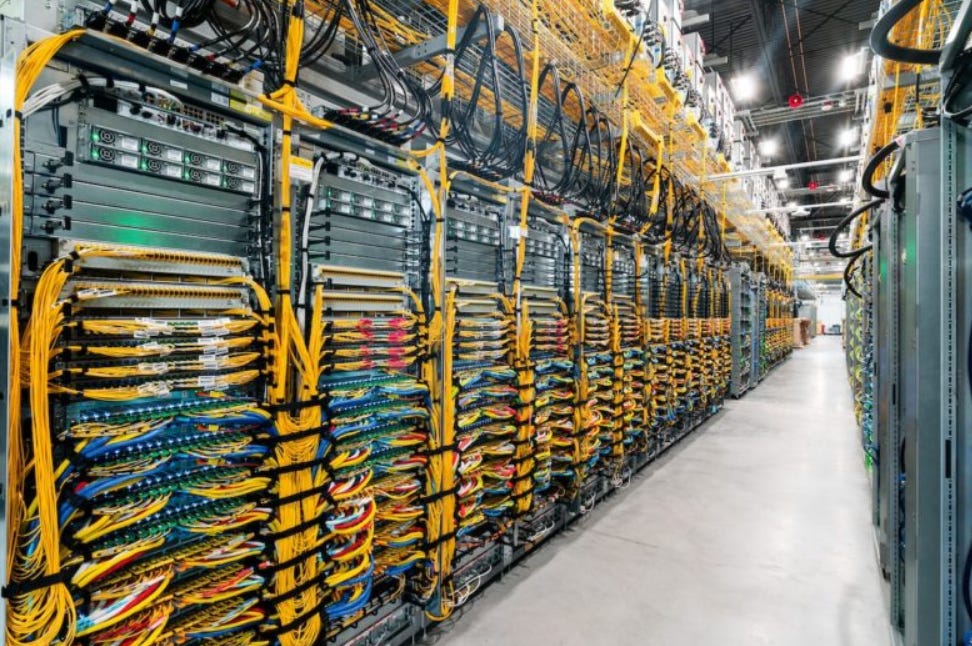
There have indeed been market rumors suggesting that Google’s internal planning around HBM procurement did not perfectly align with supply realities, creating pressure on resource allocation and deployment timelines. The specific details may not be fully public, but one fact is hard to dispute:
Even one of the world’s most capitalized, technologically advanced, and largest AI compute users cannot dictate the supply cadence of HBM.
This reveals a deeper truth about the semiconductor industry:
HBM is not a standardized commodity — it is a process-bound, capacity-concentrated form of infrastructure-in-a-component.
For Google, the role is not merely to “buy chips and run models,” but to build an AI infrastructure platform that is scalable over the long term, with predictable cost curves and controllable risk. When memory supply becomes an external variable — and that variable:
Expands capacity slowly
Is controlled by a small number of vendors
Exhibits significant price volatility
Is locked into a specific technology roadmap
— it ceases to be a procurement issue and becomes a system-architecture-level structural risk.
Consider the implications: you design your data center rack density, power distribution, cooling systems, and TPU deployment schedule — only to have expansion delayed because memory supply falls short. For a company whose core advantage is scale, this is equivalent to handing growth control to external actors.
Under such pressure, engineering teams tend to respond in a very characteristic way:
If the supply chain cannot be optimized, redesign the system so it no longer depends on it.
This is the real meaning behind the statement:
“If the building materials aren’t available, change the architectural blueprint.”
It is not an emotional reaction, but a rational systems-engineering decision. When a component shifts from being a technical option to a supply-chain bottleneck, it will be reclassifi
The Core Idea: Decoupling Memory from the Compute Die
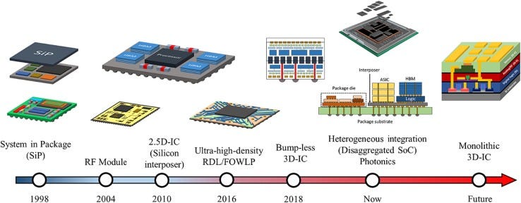
For decades, high-performance processor design followed a simple rule:
The closer the memory is to the compute core, the better the performance.
This principle drove the evolution from off-board DRAM → on-board DIMMs → on-package memory → finally HBM stacked directly beside the processor die. Each step shortened electrical distance, reduced latency, and increased bandwidth density.
But in AI systems, that rule has started to collide with physical and economic limits.
Why “Closer is Better” Is Breaking Down
Keeping memory physically adjacent to the compute die brings three structural consequences:

Package Real Estate Becomes the Bottleneck
Interposer area, bump pitch, and routing density limit how much HBM can be placed next to the processor. Bandwidth scales with proximity, but capacity does not scale proportionally.
Thermal Coupling Intensifies
AI accelerators already operate near power-density limits. Stacked HBM shares thermal paths with the logic die, creating heat concentration zones that complicate cooling.
Supply Chain Rigidity Increases
When memory is package-bound, every system expansion depends on advanced packaging capacity (TSV, interposers, stacking yield). Memory ceases to be modular infrastructure and becomes a fixed component of silicon.
At this point, “closer” begins to mean “tighter constraints.”
Google’s Architectural Reframe
Google is investigating a radical shift:
Move memory from the package level to the data-center level.
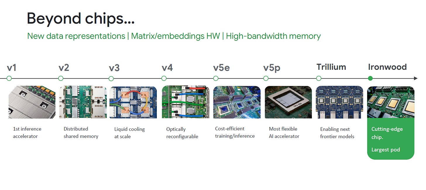
Instead of treating memory as an extension of the chip, the idea is to treat memory as a shared infrastructure resource, similar to how storage evolved from local disks to networked storage arrays.
Large DRAM pools would reside in dedicated memory racks, physically separated from the TPU. Compute nodes would access memory over high-speed optical interconnects rather than copper traces on an interposer.

Turning Disaggregated Memory into a First-Class Compute Resource
As AI models grow beyond the physical limits of on-package HBM, system architects are rethinking a long-standing assumption: memory must sit next to the compute die. The emerging alternative is memory disaggregation—pooling large amounts of DRAM outside the accelerator and accessing it optically, while preserving near-local performance semantics.
Making this viable requires three tightly coupled technologies: CPO, CXL, and OCS
CPO (Co-Packaged Optics): Breaking the Copper Wall
What it does
CPO integrates optical engines directly into the compute package (TPU/GPU/ASIC), converting electrical signals to optical signals at the chip boundary. This eliminates long copper traces, which are increasingly limited by signal loss, power consumption, and reach at 800G–1.6T speeds.
Why it matters for memory
Enables meter- to rack-scale reach without retimers
Delivers higher bandwidth density per watt than copper
Makes external memory latency predictable and scalable
In a remote-memory architecture, CPO is what allows memory trays to exist outside the accelerator chassis without collapsing power efficiency.

CXL (Compute Express Link): Making Memory Coherent

What it does
CXL provides the memory-coherency protocol that allows external DRAM to behave like an extension of system memory rather than a slow I/O device.
Why it matters for AI systems
External memory is cache-coherent, not copied
Enables load/store semantics, not DMA-style access
Allows large DRAM pools to be shared across accelerators
Without CXL, remote memory would look like storage. With CXL, it looks like RAM that happens to be far away.


Marvell Structera CXL devices effectively allow cloud operators and system designers to add extra memory, memory bandwidth, and/or computing cores to servers by transforming an open PCIe interface into a memory channel. A first-of-its kind device, the Structera A memory accelerator provides a path for adding up to 16 server CPU cores, 200Gb of memory bandwidth and 4TB of memory for offloading the processing of deep learning recommendation models (DLRM) and other tasks for CPUs.
OCS (Optical Circuit Switching): Memory on Demand
What it does
OCS dynamically establishes optical paths between compute nodes and memory pools—without packetization or electrical switching. Paths are circuit-level, low-latency, and power-efficient.
Why it matters
Memory resources can be allocated dynamically
Idle DRAM can be reassigned across workloads
The data center becomes reconfigurable, not static
With OCS, the system starts to resemble a distributed supercomputer, where topology adapts to workload needs in real time.


3月19日
3月26日
System-Level Impact: From Servers to Memory Fabrics
When CPO + CXL + OCS are combined:
Memory is no longer fixed to a single accelerator
Capacity scales independently from compute
Utilization improves dramatically
AI clusters shift from server-centric to fabric-centric design
Hyperscalers such as Google and Microsoft are already exploring variations of this model in next-generation AI infrastructure.
This architecture is not just about memory expansion—it represents a philosophical shift in data-center design:
Compute becomes elastic. Memory becomes a pool.
And the data center starts to behave like one giant, reconfigurable machine.
“Remote memory that feels local” is no longer a theoretical idea—it is rapidly becoming a cornerstone of next-generation AI systems.
Performance vs. Capacity: A Strategic Trade-off
This approach is not free. Optical conversion and protocol encapsulation introduce small latency and efficiency penalties — perhaps a few percent.
But the gain is transformative: memory capacity freedom.
Instead of being limited to a few hundred gigabytes per accelerator, effective addressable memory could scale far beyond what local HBM stacks allow. For inference workloads involving trillion-parameter models, “fit” can be more economically valuable than marginal speed gains.

3月16日
Not a Rejection of HBM — But Leverage
Google has not abandoned HBM. For extreme training scenarios, its bandwidth advantage remains unmatched. But developing an alternative architecture changes the power dynamic.
If a hyperscaler can demonstrate that it has a credible path to decouple from HBM, it is no longer just a buyer in line for supply — it becomes a negotiating force.
This is less about defeating HBM and more about reclaiming architecturalchoice. Control over AI infrastructure increasingly depends not just on who designs the fastest chips, but on who controls the memory architecture those chips rely on.
In that sense, the future of AI hardware may be decided not only in fabs and model labs, but in how we rethink the relationship between compute, memory, and the data center as a unified system.
SemiVision Viewpoint
From SemiVision’s perspective, the next phase of AI infrastructure will not be defined by compute density alone, but by memory elasticity, interconnect architecture, and supply-chain optionality. HBM will remain indispensable for the highest-performance AI training systems, but its cost structure, packaging complexity, and concentrated supplier base mean that hyperscalers cannot rely on HBM scaling as the only path forward. The strategic direction is clear: AI systems are moving from chip-centric optimization toward fabric-level architecture, where CPO, CXL, OCS, advanced packaging, and disaggregated memory together redefine the boundary between processor, memory, and data center. In this new landscape, the winners will not simply be those who secure more HBM capacity, but those who can redesign the system architecture to reduce single-point dependencies and turn memory from a bottleneck into a scalable infrastructure layer.

For Taiwan’s semiconductor ecosystem, this shift is especially important: it creates new opportunities not only in advanced packaging and silicon photonics, but also in substrates, optical engines, testing, thermal materials, and system-level integration. The memory bottleneck is therefore not just a constraint — it is a signal that the AI hardware value chain is entering a new architectural cycle.

2025年10月13日
Thanks for reading SEMIVISION @_@! This post is public so feel free to share it.


PreviousNext