TSMC 2026 Technology Symposium Hsinchu: From Transistor Scaling to System-Level AI Infrastructure
本頁目錄
TSMC 2026 Technology Symposium Hsinchu: From Transistor Scaling to System-Level AI Infrastructure
- Source: SemiVision
- Author: SEMIVISION
- Published: 2026-05-14T16:46:59+08:00
- URL: https://tspasemiconductor.substack.com/p/tsmc-2026-technology-symposium-hsinchu (1) TSMC 2026 Technology Symposium Hsinchu: From Transistor Scaling to System-Level AI Infrastructure


TSMC 2026 Technology Symposium Hsinchu: From Transistor Scaling to System-Level AI Infrastructure
This article was adapted and rewritten based on TSMC’s official press release provided to the media

May 14, 2026
∙ Paid
TSMC 2026 Technology Symposium Hsinchu: From Transistor Scaling to System-Level AI Infrastructure
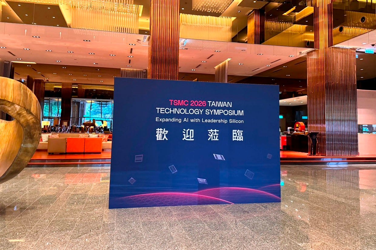
Sheraton Hsinchu Hotel 2026/05/14
The TSMC 2026 Technology symposium sends a very clear message: the semiconductor industry is no longer entering a normal technology cycle. It is entering a new system architecture cycle driven by artificial intelligence. AI is moving from generative AI to agentic AI, and then toward physical AI, where intelligence will increasingly interact with the real world through robots, vehicles, sensors, industrial systems, and edge devices.
This transition is changing the definition of semiconductor leadership. In the past, the industry mainly competed on transistor density, wafer capacity, and process node migration. In the AI era, leadership is becoming more complex. It now requires advanced logic, high-bandwidth memory integration, 2.5D and 3D packaging, optical interconnect, power delivery, thermal management, manufacturing scale, and sustainability. TSMC’s 2026 roadmap shows that the company is trying to extend its advantage from wafer manufacturing into full-system enablement.

The market implication is equally important. The semiconductor market was previously expected to reach the US$1 trillion milestone by 2030. TSMC now expects the market to cross US$1 trillion this year and expand to US$1.5 trillion by 2030. The majority of this growth will come from HPC and AI, which are expected to account for roughly 55% of the semiconductor market. Smartphones will remain important at around 20%, while automotive and IoT will each represent around 10%.

This means the center of gravity of the semiconductor industry is shifting. The smartphone cycle once defined the leading-edge semiconductor roadmap. Now, AI infrastructure is becoming the dominant driver. The key question is no longer only how many mobile processors can be shipped, but how much compute, memory bandwidth, interconnect density, and power efficiency can be delivered at the system level.
AI Inference Becomes the Next Semiconductor Demand Engine
The first phase of the AI boom was dominated by training. Large models required massive compute clusters, high-end GPUs, HBM, networking, and advanced packaging. But as AI moves from model training to broad deployment, inference is becoming increasingly important.
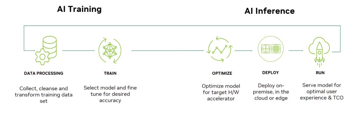
Inference is where trained AI models generate text, images, video, code, decisions, and actions. Tokens are the economic unit of this new AI infrastructure. Every token processed by a large language model represents computation, memory movement, networking, and energy consumption. As AI applications become embedded in enterprise software, consumer devices, autonomous systems, manufacturing, healthcare, and robotics, inference demand will grow continuously.
This creates a positive feedback loop. More AI capability improves productivity and creates more value. More value leads to more investment in AI systems. More AI systems require more silicon. In this cycle, the semiconductor industry becomes the physical foundation of the intelligence economy.
For TSMC, this is not just a demand story. It is a technology roadmap story. AI requires not only faster chips, but also larger packages, more HBM stacks, better power integrity, shorter interconnects, and eventually optical I/O. This is why the 2026 forum placed equal emphasis on advanced logic, 3DFabric, SoW, SoIC, and COUPE.

4月7日
A14 and A13: Extending Logic Scaling into the AI Era
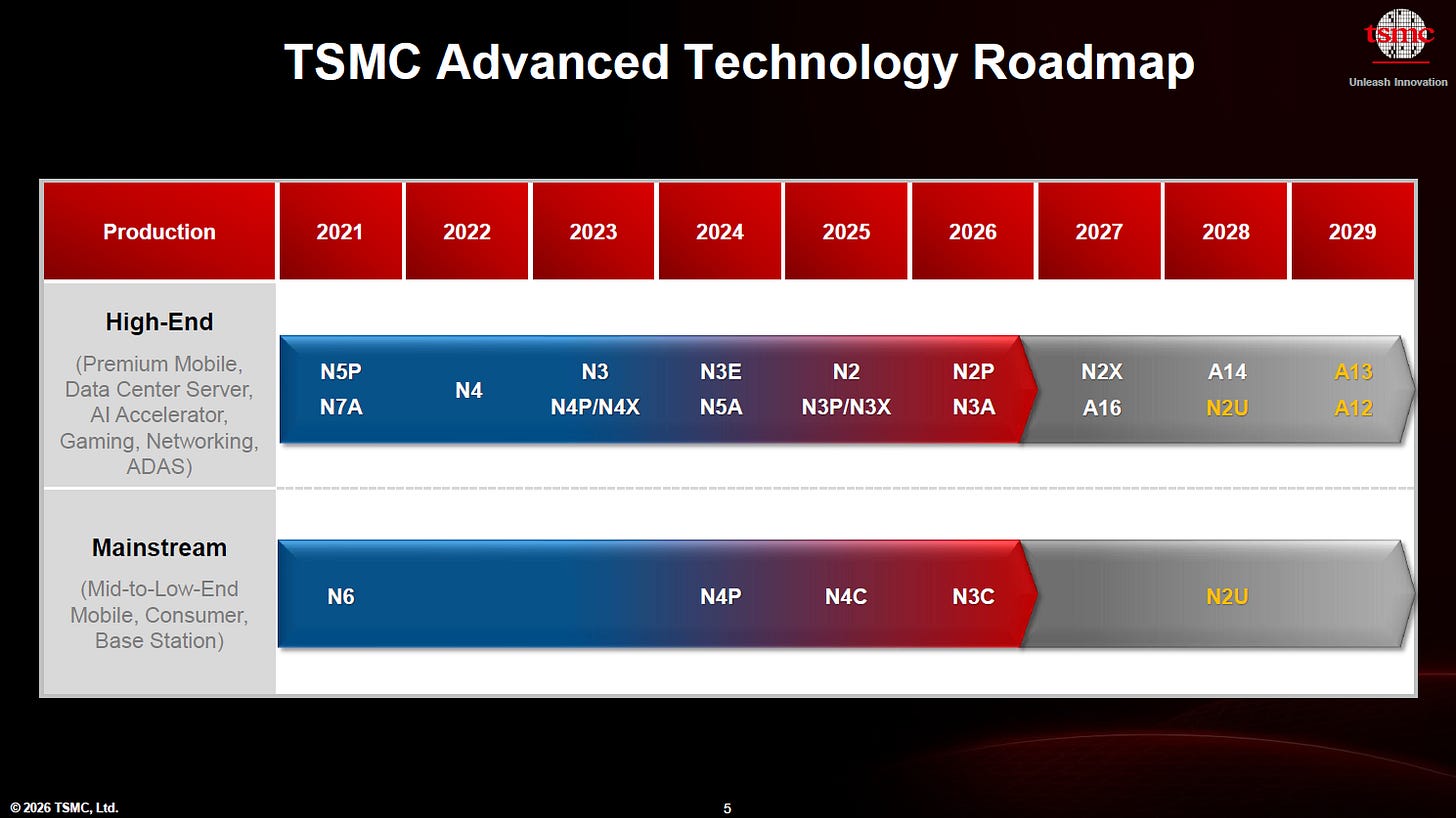
On the advanced logic side, TSMC continues to push beyond N2 into the angstrom era. A14 will be TSMC’s second-generation nanosheet transistor technology and will use NanoFlex Pro to improve power, performance, and area.
Compared with N2, A14 is expected to deliver up to 15% speed improvement at the same power, up to 30% power reduction at the same speed, around 1.23 times logic density, and approximately 1.2 times chip density. A14 is scheduled for volume production in 2028.
The importance of A14 is not only the raw PPA improvement. It represents TSMC’s attempt to keep logic scaling relevant in an era where system-level bottlenecks are becoming more visible. For AI and HPC, the value of each process node must be evaluated not only by transistor density, but also by its interaction with power delivery, SRAM, package size, HBM integration, and cooling.
A13 is positioned as a direct shrink of A14. Its design rules are fully backward-compatible, allowing customers to migrate A14 designs more quickly to A13. Compared with A14, A13 is expected to save around 6% area while providing additional power and performance benefits through design-technology co-optimization. A13 is planned for production in 2029, one year after A14.

This is strategically important. In advanced nodes, design cost and time-to-market are becoming critical constraints. A backward-compatible migration path can reduce friction for major customers, especially those building large AI accelerators, smartphone SoCs, and HPC chips. In other words, A13 is not only a smaller node. It is also a roadmap continuity tool.

4月23日
N2 Family: Building a Wider Platform, Not Just One Node
TSMC’s N2 family is becoming a broad technology platform. N2 began volume production in the fourth quarter of 2025. N2P is scheduled for production in the second half of 2026, while A16 with Super Power Rail is also expected to be production-ready in the second half of 2026.
The introduction of Super Power Rail is especially relevant for AI and HPC. As chips become larger and more power-hungry, power delivery is no longer a back-end detail. It is a fundamental design constraint. Better power delivery can improve voltage stability, reduce IR drop, and support higher-performance logic at lower power.
TSMC also highlighted ultra-high-performance three-plate metal-insulator-metal capacitors, with capacitance density exceeding 500 fF/μm². This is not a minor feature. For AI/HPC processors, power integrity is becoming one of the most important design issues. Large AI chips can experience extreme transient current demand. On-chip and package-level decoupling solutions will become increasingly valuable.
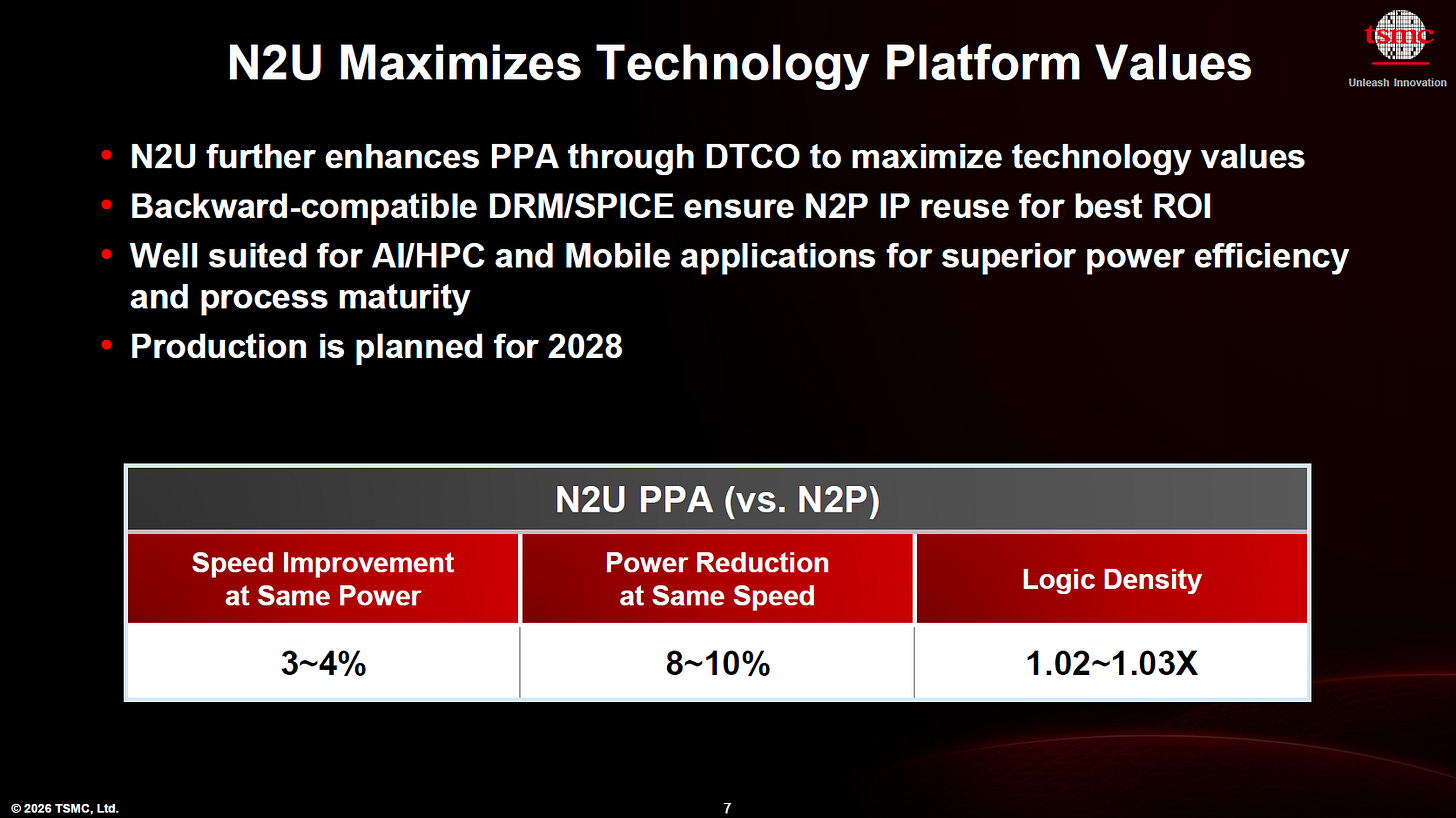
Beyond N2P, TSMC plans to introduce N2X and N2U. N2X is scheduled for 2027, while N2U is planned for 2028. N2U is an extension of N2P using design-technology co-optimization, targeting AI/HPC and smartphone applications. Compared with N2P, N2U is expected to provide 3–4% speed improvement, 8–10% power reduction, and up to 3% logic density improvement.
This suggests that TSMC is moving from a single-node strategy toward a family-based platform strategy. Different customers need different trade-offs. AI accelerators, mobile SoCs, automotive processors, and edge AI chips do not optimize for the same metrics. The node family must become more segmented and application-specific.
Beyond Nanosheets: CFET as the Next Scaling Candidate
TSMC also discussed technology beyond nanosheets. The transistor roadmap has moved from planar devices to FinFETs, and now to nanosheets. After nanosheets, the next major candidate is CFET, or complementary field-effect transistor, which vertically stacks nFET and pFET devices.
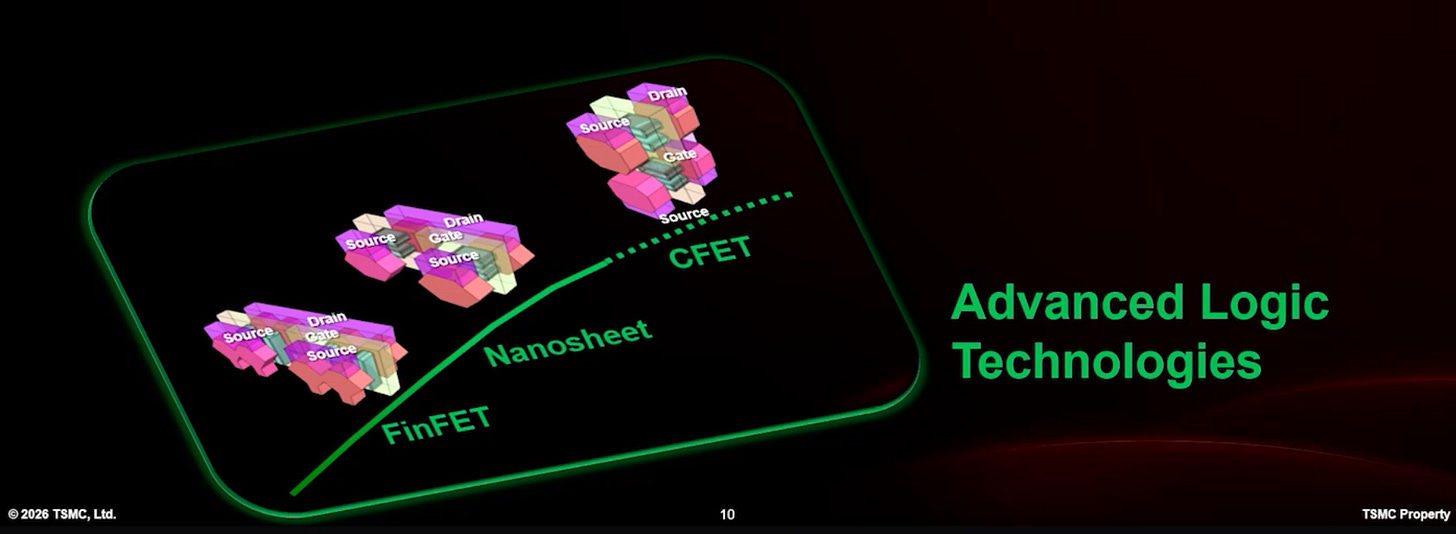
CFET is important because traditional lateral scaling is becoming increasingly difficult. If nFET and pFET can be stacked vertically, standard cell area can be reduced without relying only on two-dimensional shrink. TSMC demonstrated a working 6T SRAM cell with around 30% smaller footprint compared with conventional nanosheet designs under similar design rules. The company also demonstrated CFET ring oscillators with around 1,000 transistors.
These are still technology demonstrations, not near-term production announcements. But they show the direction of future scaling. After A14 and A13, transistor architecture innovation will become even more difficult and expensive. CFET may become one of the key candidates to continue density scaling, especially for logic and SRAM-intensive designs.
CoWoS: AI Packaging Moves Toward Larger and Larger Systems
If advanced logic is one pillar of AI computing, advanced packaging is the second pillar. TSMC’s CoWoS technology has become a key enabler of both AI training and inference. The reason is simple: AI processors need to sit very close to HBM. Without high-bandwidth, low-latency memory access, compute units cannot be fully utilized.

This year, TSMC announced production of the world’s largest 5.5-reticle-size CoWoS, with yield exceeding 98%. Over the next five years, CoWoS will continue to scale package size every year to integrate more logic and HBM dies.
The roadmap is aggressive. A 14-reticle-size CoWoS capable of integrating 20 HBM stacks is expected to enter volume production in 2028. A version larger than 14 reticles, capable of integrating 24 HBM stacks, is expected to be ready in 2029.
This reflects a structural change in AI hardware. The AI accelerator is no longer just a chip. It is becoming a package-level system. More HBM stacks mean higher memory bandwidth and larger model capacity. Larger interposers mean more routing complexity, more warpage control challenges, and higher requirements for substrate, underfill, thermal interface materials, and inspection.
For the supply chain, this opens a new competitive field. Materials, substrates, bonding equipment, metrology, thermal solutions, and advanced PCB technologies will become increasingly strategic. The bottleneck is moving from transistor count alone to package-level system integration.

5月5日
SoW: Wafer-Level Integration for Extreme AI Systems
TSMC’s System-on-Wafer, or SoW, represents an even more ambitious direction. SoW is a wafer-level integration technology designed to combine logic and HBM dies for AI training systems that require extreme compute density.
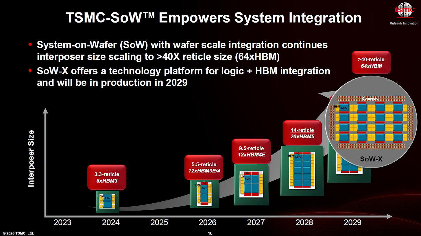
SoW allows interposer size to scale beyond 40 reticle sizes. It can integrate up to 64 HBM stacks and 16 compute dies. This is not conventional packaging anymore. It is closer to wafer-level system construction.
SoW-P, used for logic die integration, has been in production since 2024. The more advanced SoW-X, which integrates logic and HBM dies, is expected to be ready in 2029.
The strategic meaning is clear. As AI model scale continues to grow, chip-level design will not be enough. The industry needs new ways to create larger compute fabrics with shorter communication paths and higher bandwidth. SoW could become one of the possible platforms for ultra-large AI training systems.
However, this direction also introduces major challenges. Wafer-level integration requires extremely high yield management, advanced thermal design, repair strategies, power delivery, and system-level test. It also changes the economics of semiconductor manufacturing. The value is no longer only in each die, but in the entire wafer-scale system.

5月7日
SoIC: 3D Integration Becomes a Mainstream Scaling Tool
TSMC’s SoIC technology provides another important path: 3D interconnect. Compared with 2.5D CoWoS interconnect, SoIC offers 56 times higher connection density and 5 times better power efficiency.
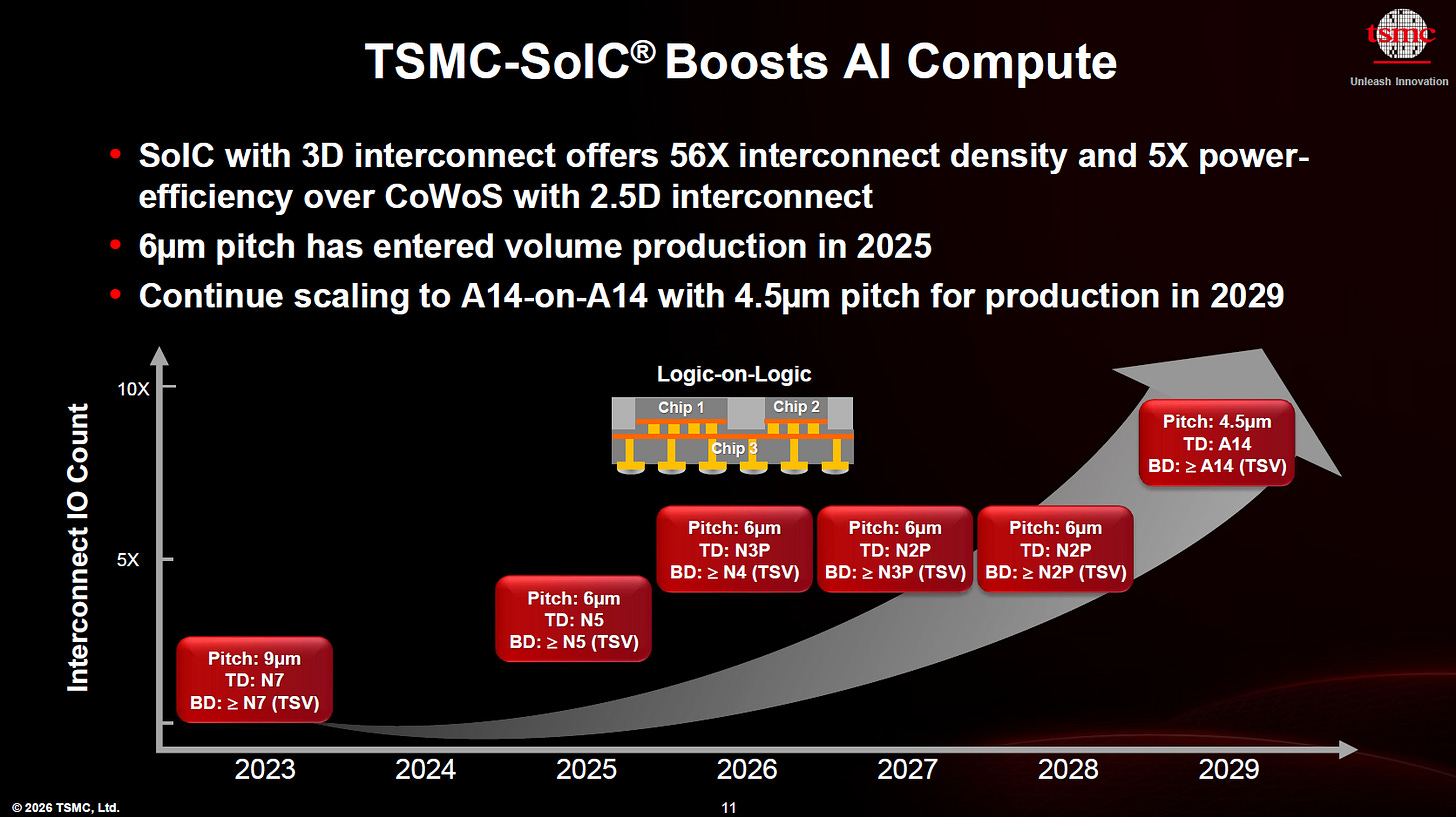
N7-to-N7 SoIC with 9μm bond pitch has been in production since 2023. A 6μm bond pitch version entered production in 2025. The roadmap continues with N2-to-N2 stacking at 6μm bond pitch in 2028, followed by A14-to-A14 stacking with 4.5μm bond pitch in 2029.
This is a critical trend. In the AI era, 3D integration can reduce data movement energy by shortening interconnect distance. It can also allow logic, SRAM, cache, analog, and potentially specialized accelerator blocks to be stacked more efficiently.
But SoIC also raises the bar for design methodology. Thermal coupling, stress management, known-good-die strategy, hybrid bonding yield, and EDA support will become essential. The future of chip design will increasingly require co-optimization across process, package, architecture, and system software.

2025年7月13日
COUPE: Optical I/O Becomes Part of the AI Roadmap
One of the most forward-looking parts of TSMC’s forum is COUPE, the Compact Universal Photonic Engine. This technology is designed to support co-packaged optics solutions.

Compared with traditional copper interconnects, CPO using COUPE on a substrate can provide 4 times better power efficiency and 90% lower latency. When COUPE is integrated on an interposer, performance can improve further, reaching 10 times better power efficiency and 95% lower latency.
This is extremely important. AI clusters are becoming increasingly limited by data movement. Copper interconnects face serious challenges in power consumption, signal integrity, reach, and latency as bandwidth rises. Optical I/O is becoming a system-level necessity, not just a networking option.
TSMC expects the world’s first 200Gbps micro-ring modulator using COUPE technology to enter production in 2026. The company also plans to scale toward 400Gbps modulators, multi-wavelength technology, and multi-row fiber array units, targeting 4Tbps/mm bandwidth density by 2030.
This indicates that silicon photonics is moving closer to the core of advanced packaging. In the future, optical engines may become part of the AI package, interposer, or system fabric. This would reshape the boundaries between foundry, OSAT, optical module vendors, PCB makers, and system companies.

2025年11月29日
Specialty Technologies: Automotive, RF, Memory, and Display
Although AI and HPC dominate the roadmap, TSMC also emphasized specialty technologies.
In automotive, N3A is positioned as the most advanced logic process for automotive applications, with more than 10 tape-outs expected. N3A automotive qualification was completed in the fourth quarter of 2025. TSMC is also preparing N2P Auto-Use PDKs for autonomous vehicles and physical AI applications. N2A, based on N2P, will become the first nanosheet technology for automotive applications and is expected to qualify in the first quarter of 2028.

For RF, N4CRF is TSMC’s most advanced RF CMOS technology. Compared with N6 RF+, N4CRF provides 39% lower power and 33% smaller area for digital-intensive RF SoCs used in smartphones and AI glasses. This is important because future wearable AI devices will require compact, power-efficient RF and compute integration.
In non-volatile memory, TSMC is moving RRAM and MRAM from 40/28/22nm toward 16/12nm. RRAM at 40/28/22nm has been in production since 2022, while 12nm RRAM is ready for customer tape-out. Automotive-grade RRAM at 28/22nm has already passed Grade 1 qualification, and 12nm RRAM Auto is expected by the end of 2026. MRAM at 22nm is in production, while 16nm MRAM is ready for customer tape-out. A 12nm MRAM solution for higher logic density and performance is under development and expected to be ready by the end of 2026.
In display technologies, TSMC introduced the industry’s first FinFET high-voltage platform for foldable OLED, thin OLED, and AR glasses. Compared with N28HV, N16HV is expected to increase gate density by 41% and reduce power by 35% for high-end smartphones. For near-eye display engine backplanes, N16HV can reduce die area by 40% and power by 20% compared with 28nm.
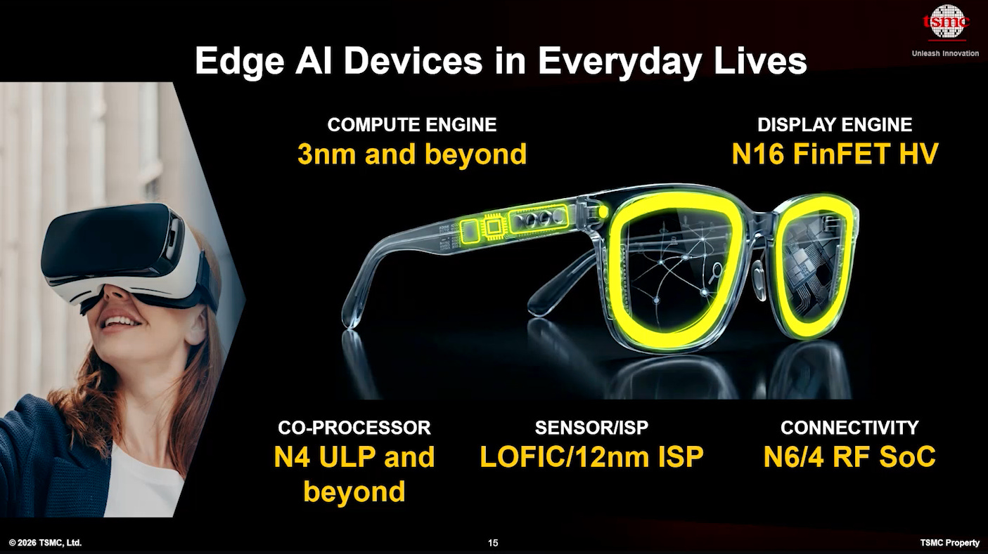
These specialty platforms show that TSMC is not only serving leading-edge AI accelerators. It is also building technology foundations for automotive intelligence, AI wearables, advanced displays, embedded memory, and RF integration.
Manufacturing Scale: The Real Barrier to Entry
Technology leadership is only meaningful if it can be manufactured at scale. TSMC highlighted several important capacity expansion targets.
N2/A16 capacity is expected to ramp rapidly, with a compound annual growth rate of 70% from 2026 to 2028. From 2022 to 2027, TSMC plans to expand N3 and N5 capacity at a 25% CAGR. The company also expects first-year N2 chip output to be 45% higher than N3 at the same stage, reflecting stronger integration between R&D and manufacturing.

AI accelerator demand from TSMC customers is expected to grow 11 times from 2022 to 2026. Demand for large-die wafers is expected to grow 6 times. Meanwhile, CoWoS and SoIC capacity is expected to grow at more than 80% CAGR from 2022 to 2027.

This is perhaps the most important business message. TSMC’s moat is not only process technology. It is the ability to convert process technology into large-scale, high-yield manufacturing. In AI semiconductors, this capability is even more valuable because customers need advanced logic, advanced packaging, HBM integration, and capacity assurance at the same time.
Green Manufacturing and ESG: Sustainability Becomes Part of Technology Competitiveness
TSMC also emphasized responsible and sustainable innovation. The company remains committed to reaching net-zero emissions by 2050 based on science-based targets and absolute reduction measures. In 2025, TSMC reduced emissions by 38,000 metric tons of CO₂ equivalent.

For resource circularity, TSMC aims to reach a 70% in-house resource recycling rate by 2030 through new fab infrastructure and zero-waste manufacturing centers. In 2025, the company achieved a 33% in-house resource recycling rate through zero-waste manufacturing centers and specialty chemical reuse.
For water management, TSMC aims to achieve 100% water positive impact by 2040 through regional solutions, including reclaimed water in Taiwan, groundwater replenishment in Kumamoto, Japan, and industrial reclaimed water in Arizona. In 2025, TSMC achieved 20% water positive impact and 18% reclaimed water usage.

This matters because advanced semiconductor manufacturing is resource-intensive. As fabs expand globally, power, water, chemicals, land, and community impact will become increasingly important constraints. Sustainability is no longer only a corporate responsibility issue. It is becoming part of operational resilience and customer trust.

4月9日
SemiVision View: TSMC Is Redefining the Foundry Model
The 2026 Technology Forum shows that TSMC is no longer just presenting a process roadmap. It is presenting a system roadmap.
A14 and A13 extend transistor scaling. N2, N2P, N2X, N2U, and A16 create a broader logic platform. CoWoS expands AI package size. SoIC improves 3D interconnect density. SoW pushes integration toward wafer-scale systems. COUPE brings optical I/O into the packaging roadmap. Specialty technologies support automotive, RF, embedded memory, and display applications. Manufacturing scale and sustainability provide the operational foundation.
The key message is that future semiconductor competition will not be won by one technology alone. It will be won by the company that can integrate logic, memory, packaging, optics, power, thermal, manufacturing, and ecosystem support into one coherent platform.
For AI infrastructure, this means the semiconductor value chain is entering a new phase. The next bottleneck may not be only EUV, transistors, or HBM supply. It may be the ability to integrate all components into a manufacturable, scalable, power-efficient system.

That is why TSMC’s 2026 forum is significant. It shows that the company is preparing for a future where the chip is no longer the final product. The package becomes the system. The wafer becomes the platform. And the foundry becomes the infrastructure provider for the global intelligence economy.

There is a small interactive activity at today’s event venue where visitors can test how much they know about TSMC’s advanced packaging technologies. Everyone is welcome to give it a try.


PreviousNext