TSMC’s U.S. Expansion Enters a New Phase: Redefining the Global Advanced Manufacturing Map
TSMC’s U.S. Expansion Enters a New Phase: Redefining the Global Advanced Manufacturing Map
- Source: SemiVision
- Author: SEMIVISION
- Published: 2026-05-08T22:10:49+08:00
- URL: https://tspasemiconductor.substack.com/p/tsmcs-us-expansion-enters-a-new-phase (1) TSMC’s U.S. Expansion Enters a New Phase: Redefining the Global Advanced Manufacturing Map


TSMC’s U.S. Expansion Enters a New Phase: Redefining the Global Advanced Manufacturing Map
Original Article By SemiVision Research [Reading time: 11mins]

May 08, 2026
∙ Paid
TSMC’s U.S. Expansion Enters a New Phase: Redefining the Global Advanced Manufacturing Map
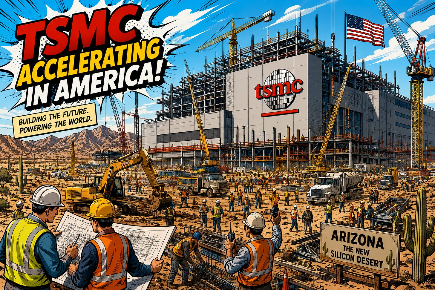
TSMC’s U.S. footprint is entering another stage of expansion, signaling that the global semiconductor industry is moving into a new phase. Advanced process technology is no longer only a technology race; it has become a comprehensive competition involving geopolitics, customer trust, supply chain resilience, and capital allocation capability.
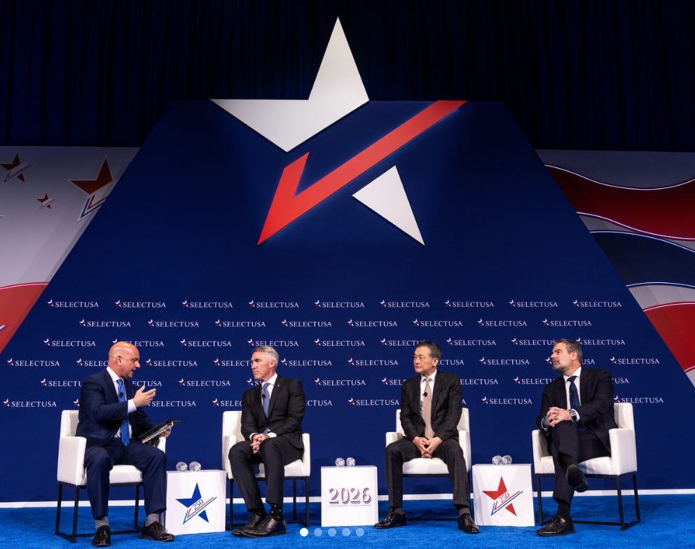
According to reports, TSMC Senior Vice President and Co-Chief Operating Officer Dr. Cliff Hou stated at the SelectUSA Investment Summit that the company is prepared for any new business opportunities. The market has interpreted this as a sign that TSMC may further expand its investment in the United States. At the same time, TSMC plans to amend its corporate charter to raise the maximum number of board seats to 12, a move widely viewed as a governance adjustment in response to the company’s increasingly complex global operations. Related reports also suggest that if TSMC’s U.S. expansion continues, its total investment scale could potentially reach as high as US$250 billion.

From US$65 Billion to US$165 Billion, and Now Toward the Market’s US$250 Billion Imagination
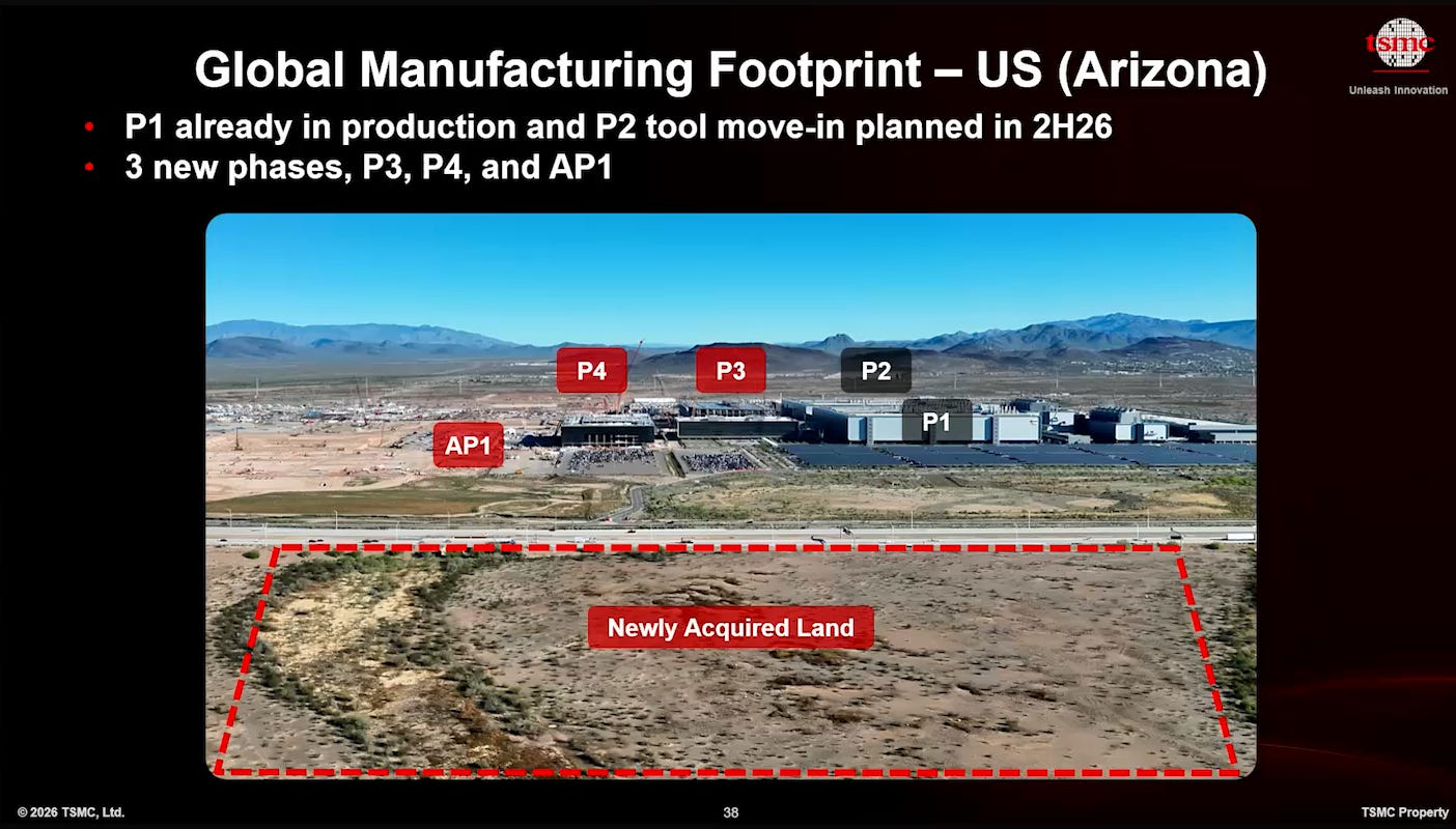
The evolution of TSMC’s U.S. investment is no longer a one-off fab construction plan. It is becoming the formation of a long-term industrial base. In 2025, TSMC officially announced that it would add another US$100 billion on top of its original US$65 billion investment, bringing its total U.S. investment to US$165 billion. The plan includes three additional wafer fabs, two advanced packaging facilities, and a major R&D center. This means TSMC’s role in the United States has evolved from an overseas production site into a second advanced manufacturing cluster.
2025年3月4日
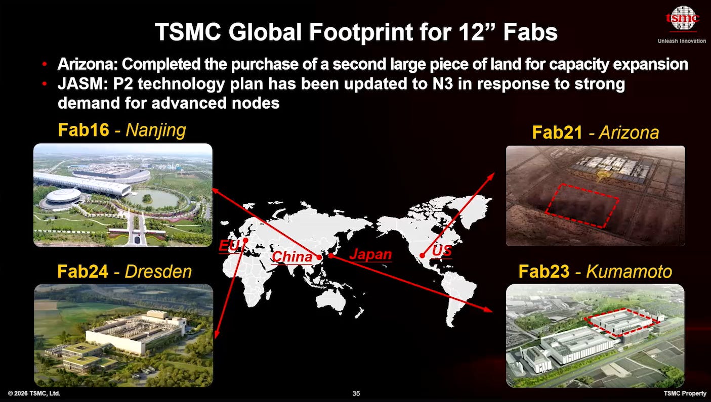
If the market’s rumored US$250 billion potential scale further materializes, it would imply that TSMC’s U.S. layout may go beyond the existing P1 to P6 fabs and AP1/AP2 packaging facilities, moving toward a more complete gigafab cluster. Reuters has also reported that TSMC has completed the purchase of a second parcel of land in Arizona to increase future expansion flexibility and respond to AI-related demand. This is highly significant because land is not a short-term financial investment. It is a strategic option on capacity, customers, and policy conditions over the next decade or more.
U.S. Manufacturing Is Not the Lowest-Cost Solution, but a Necessary Solution Driven by Customers and Policy
From a pure manufacturing cost perspective, the United States is not the most ideal expansion location for TSMC. Fab construction costs, labor costs, engineering costs, regulatory costs, supply chain support costs, and depreciation pressure are generally higher in the United States than in Taiwan. This is why TSMC has long insisted on keeping Taiwan as the core base for advanced process manufacturing, building an efficiency model that other countries find difficult to replicate through dense supply chains, engineering culture, and process learning curves.
But today’s issue is no longer just cost. AI chips are becoming national strategic assets. Advanced process capacity is no longer only commercial capacity; it is the foundational capability behind technological sovereignty, defense security, cloud infrastructure, and the digital economy. The U.S. government wants more critical semiconductor manufacturing to return onshore, while U.S. cloud and AI customers also want to reduce single-region geopolitical risk. Under this structure, TSMC’s investment in the United States may sacrifice part of its manufacturing efficiency, but it gains higher-level customer stickiness, policy security, and market access.
This is why TSMC’s U.S. investment should not be judged only by whether the cost is high. It should be evaluated by whether it can preserve the long-term trust of the world’s largest AI customer base. For customers such as NVIDIA, AMD, Apple, Broadcom, Amazon, Google, and Microsoft, advanced process technology is not merely wafer supply. It is a core variable in their AI infrastructure roadmaps for the next decade.
Arizona Is Not Just About Wafer Fabs, but a Combined Play of Advanced Process and Advanced Packaging
The most important aspect of TSMC’s U.S. expansion is that advanced packaging is now being incorporated into the same strategic narrative. In the past, advanced process and advanced packaging were often discussed separately. Front-end process technology determined transistor density, while back-end packaging was responsible for chiplet integration. But in the AI/HPC era, this boundary is disappearing.
As AI GPUs, ASICs, HBM, I/O dies, silicon interposers, CoWoS, SoIC, and future optoelectronic integration become increasingly intertwined, system performance is no longer determined solely by the process node of a single logic die. Instead, it is determined by the bandwidth, power consumption, latency, thermal performance, and yield of the entire package-level system. TSMC’s plan to build advanced packaging facilities in the United States shows that it does not want the U.S. to be merely a wafer-out manufacturing location. It wants to partially localize the AI system integration capabilities that U.S. customers care about most.
For TSMC, this is both defense and offense. On the defensive side, it responds to U.S. supply chain security requirements. On the offensive side, it uses a complete solution combining process and packaging to lock AI customers more deeply into the TSMC ecosystem. In the future, customers may not simply choose N2, A16, or A14 as a process node. They may choose an entire platform consisting of logic process, 3D integration, advanced packaging, HBM integration, and thermal solutions.

5月5日
Intel’s Threat Is Not Today’s Market Share, but the Formation of a U.S. System-Level Alternative
One important background behind TSMC’s increased U.S. investment is the presence of Intel Foundry. From a short-term market share perspective, Intel Foundry still cannot be compared with TSMC. Intel still needs time to rebuild its capabilities in external customer mass production, advanced process yield, design ecosystem, EDA/IP completeness, and customer trust. But from SemiVision’s perspective, Intel’s threat is not whether it can immediately take advanced process orders away from TSMC today. The real question is whether it can become the “second system-level supply chain” in the eyes of the U.S. government and U.S. hyperscalers.
Intel’s competitive weapon is not a single process node. It is the combination of 18A, 14A, EMIB, Foveros, advanced packaging, U.S.-based manufacturing, and the x86/AI system ecosystem. Market rumors have repeatedly suggested that major customers such as NVIDIA and Apple are evaluating Intel’s 18A, 14A, and advanced packaging capabilities. Industry report has also noted that the market is closely watching whether technology giants such as NVIDIA and Apple will evaluate Intel’s advanced nodes and packaging capabilities.
More importantly, Intel’s advanced packaging has particular appeal to AI ASIC customers. The future development paths of Google TPU, Amazon Trainium, Microsoft Maia, and Meta MTIA will not necessarily rely forever on a single packaging platform. When CoWoS capacity becomes tight, the reticle limit continues to approach, and HBM integration costs rise, customers will naturally seek a second source of supply. Intel’s EMIB and Foveros are not simple replacements for CoWoS, but they provide another chiplet integration path. Especially with U.S. manufacturing and U.S. government support, they carry strategic value for hyperscalers.

4月24日
Intel’s Real Opportunity Lies in Packaging, Not in Directly Replicating TSMC’s Logic Process Advantage
If Intel tries to directly challenge TSMC’s most advanced logic process in the short term, the difficulty will be extremely high. TSMC’s advantage comes from long-term mass production learning curves, customer design collaboration, supply chain density, yield control, and capital efficiency. These cannot be caught up with simply by naming one or two advanced nodes.
However, if Intel enters through advanced packaging, the threat becomes more realistic. Competition in advanced packaging is not simply about linewidth. It is about the integration of substrate, bridge, interconnect density, thermal path, power delivery, die-to-die interface, HBM placement, test flow, and system yield. Intel has accumulated long-term experience in EMIB, Foveros, and high-end CPU packaging. If it can secure commitments from AI ASIC or GPU customers, it may first penetrate through certain I/O dies, base dies, packaging services, or specific chiplet modules.
SemiWiki has also pointed out that the strategic significance of Intel Foundry lies in opening advanced process technology to external customers while combining it with U.S.-based advanced packaging capabilities such as EMIB and Foveros. This shows that Intel’s challenge is not to copy TSMC, but to position itself as a differentiated “U.S. system-level foundry.”

4月21日
TSMC’s Additional U.S. Investment Is a Preemptive Defense Against Intel’s Threat
TSMC is certainly aware of Intel’s threat. A mature industry leader does not wait until a competitor has completed its catch-up before taking defensive action. It moves before the competitor is fully formed, securing key customers, key capacity, and key policy positions in advance. TSMC’s additional investment in the United States is essentially this kind of preemptive defense.
First, TSMC wants to show the U.S. government that the most reliable localization partner for advanced process technology remains TSMC, not Intel Foundry, which is still in the process of rebuilding.
Second, TSMC wants to show U.S. customers that even if they consider supply chain diversification, they do not need to shift their core platforms substantially toward Intel, because TSMC can already provide a higher proportion of advanced manufacturing capacity in the United States.
Third, TSMC wants to prevent Intel from using “U.S.-based manufacturing” as its only differentiation point. By incorporating this political and supply chain narrative into its own global strategy, TSMC weakens Intel’s messaging advantage.
In other words, TSMC’s move into the United States is not passive compliance. It is an active effort to neutralize Intel’s narrative advantage. When TSMC also has fabs in the United States, also provides advanced process technology, also plans advanced packaging, and also supports AI customers, U.S. customers’ reasons for choosing Intel must return to technology, cost, yield, and delivery capability rather than geopolitics alone.

3月25日
Raising the Board Seat Limit Shows That TSMC Has Evolved from a Taiwanese Company into a Global Strategic Enterprise
TSMC’s plan to raise the maximum number of board seats to 12 appears on the surface to be a corporate governance adjustment. But at a deeper level, it reflects the sharp increase in TSMC’s operational complexity. In the past, TSMC’s core question was how to make the world’s best advanced process technology in Taiwan. Today, the question has become how to simultaneously manage operations across Taiwan, the United States, Japan, Europe, and other locations, while balancing different governments, different customers, different cost structures, and different levels of supply chain maturity.
When a company’s investment scale, geopolitical role, and customer influence reach this level, the board no longer only needs financial oversight. It needs comprehensive judgment across global policy, law, supply chains, capital markets, customer strategy, technology roadmaps, and risk governance. TSMC is no longer an ordinary manufacturing company. It has become one of the core contractors of global AI infrastructure.
This also means that TSMC’s future competitive risks will not only come from Samsung or Intel. They will also come from political pressure, cost structure, talent supply, cross-border management efficiency, and yield consistency after supply chain diversification. To some extent, the expansion of the board is a governance response to globalization pressure.

2月6日
Taiwan Remains the Core; the United States Is an Extension, Not a Replacement
Even if TSMC significantly increases its investment in the United States, this does not mean Taiwan’s position will be weakened. On the contrary, Taiwan will remain TSMC’s most important base for advanced process R&D, mass production learning, and supply chain collaboration. The value of the U.S. base lies in serving strategic customers, reducing geopolitical concerns, and absorbing part of the advanced manufacturing demand. It is not meant to fully replicate Taiwan’s ecosystem.
Semiconductor manufacturing cannot be replicated simply by moving equipment from one place to another. Taiwan’s advantage comes from engineer density, supplier response speed, equipment maintenance capability, materials validation efficiency, customer collaboration frequency, and a process culture accumulated over decades. This ecosystem learning curve is extremely difficult to relocate in the short term.
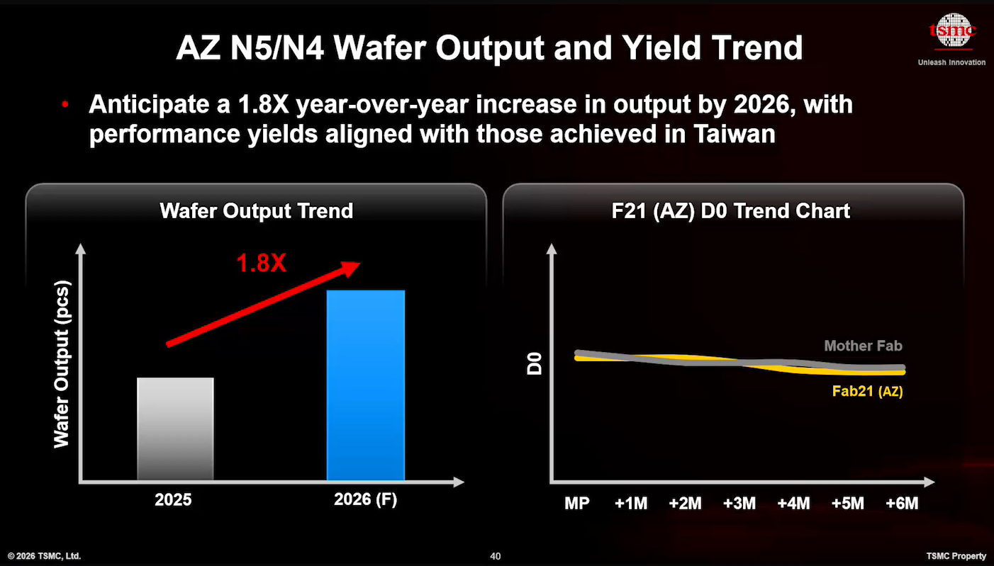
But TSMC also cannot defend Taiwan alone. In the AI era, customer demand is too large, political pressure is too strong, and global supply chains are changing too quickly. If TSMC does not establish a sufficiently large presence in the United States, Intel, Samsung, and even new supply chain combinations supported by the U.S. government will attempt to fill that space.
4月8日
Conclusion: TSMC Is Turning the United States into Its Second Moat
Intel’s threat should not be underestimated. It is not yet a full substitute for TSMC, but it could become the second platform for the U.S. AI supply chain, especially in advanced packaging, chiplet integration, and government-backed manufacturing. TSMC’s increased U.S. investment is precisely aimed at securing the U.S. market, AI customers, and the advanced packaging narrative before Intel has fully rebuilt foundry trust.
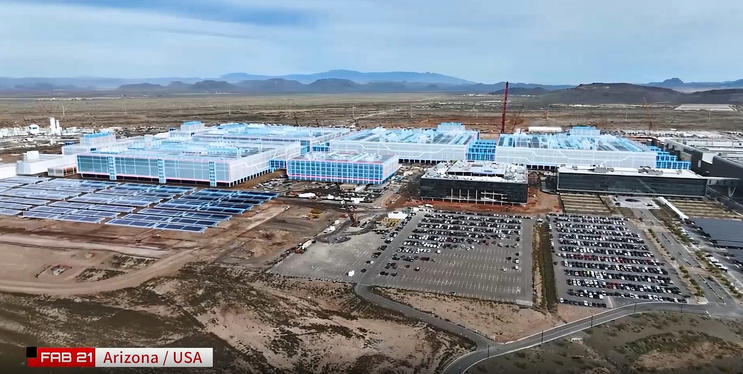
The future of semiconductor competition will no longer be only about whose transistors are smaller. It will be about who can provide the most complete, trusted, and resilient AI system manufacturing platform. TSMC’s U.S. expansion is its answer to this question: in an era when global supply chains are being redrawn, TSMC does not only want to be the world’s best foundry. It also wants to become an infrastructure layer that the U.S. AI industry cannot bypass.

4月17日
In addition, TSMC’s water stewardship strategy shows that green manufacturing is becoming a regional engineering problem, not just an internal fab efficiency target. The company aims to become 100% water positive by 2040, supported by different local solutions: reclaimed water in Taiwan, groundwater recharge in Kumamoto, and industrial reclaimed water in Arizona.

This reflects an important shift in semiconductor sustainability: as fabs expand globally, water management must be customized to each region’s climate, infrastructure, regulation, and community needs. For advanced semiconductor manufacturing, long-term competitiveness will increasingly depend not only on process technology and capacity, but also on whether fabs can secure resilient, low-impact water sources at scale.


PreviousNext