The Engineering Logic Behind TSMC’s High-NA Strategy
The Engineering Logic Behind TSMC’s High-NA Strategy
- Source: SemiVision
- Author: SEMIVISION
- Published: 2026-04-29T09:56:53+08:00
- URL: https://tspasemiconductor.substack.com/p/the-engineering-logic-behind-tsmcs (1) The Engineering Logic Behind TSMC’s High-NA Strategy


The Engineering Logic Behind TSMC’s High-NA Strategy
Original Article by SemiVision Research [Reading time: 27 mins]

Apr 29, 2026
∙ Paid

The Three Engineering Clues Kevin Zhang Left Behind
On April 22, 2026, at TSMC’s North America Technology Symposium in California, TSMC Deputy Co-COO Kevin Zhang made a remark that immediately rippled across the semiconductor industry:
“I can tell you, I’m amazed by our R&D team. They continue to find ways to scale without using High-NA. One day they may have to use it, but for now we can still benefit from the current EUV tools without going to High-NA. And you know, this tool is very, very expensive.”

That single statement shook the market.
On the same day, ASML shares in Europe fell 3.3% intraday, wiping out roughly $17 billion in market value. The market’s instant interpretation was simple:
TSMC is rejecting High-NA, and ASML’s next growth narrative just took a hit.
But framing this as “TSMC rejecting ASML” misses the real point.
TSMC is not unable to access High-NA, nor is it unprepared to evaluate it. In fact, it is probably the one company in the world most qualified to say,“not yet.”TSMC has been central to ASML’s EUV journey from the beginning: from the NXE:3100 era in 2010, to becoming part of ASML’s Customer Co-Investment Program in 2012, to already having an EXE:5000 in its Hsinchu R&D center as of September 2024. TSMC is not merely ASML’s largest EUV customer. It has been one of the core enablers of EUV mass production itself.

So when Kevin Zhang said TSMC does not need High-NA now, he was not saying“never.”
He was saying“not yet.”
That is not a political message.
It is an engineering judgment.
And behind that judgment, there are three clear engineering clues.

4月23日
Below we will share:
Clue One: TSMC Has Never Been the First to Use a New Tool
Clue Two: From A16 to A12, TSMC’s Real Pain Point Is _
Clue Three: High-NA Itself Is Still Not a Fully Mature Tool for __
What ASML Lost Is Not the Future - It Is the __
What TSMC Is Really Refusing Is Not High-NA -It Is Paying __
Three Real Takeaways for Investors
Viewpoint from SemiVision- Deep Inisght
Clarification: TSMC Has Not Avoided Buying High-NA EUV; It Is Delaying Large-Scale Deployment
It is important to clarify that TSMC has not “completely avoided purchasing” or “abandoned” High-NA EUV. Based on currently available public information, TSMC has already obtained a small number of High-NA EUV tools, mainly for R&D, process learning, and early ecosystem preparation, rather than immediate high-volume manufacturing deployment.
The real issue is not whether TSMC will buy High-NA EUV, but when TSMC will scale High-NA EUV into high-volume manufacturing.
In other words, TSMC is not saying “no” to High-NA EUV. It is choosing to delay subsequent large-scale procurement and mass-production deployment. This is a timing decision related to technology maturity, throughput, process window, the mask ecosystem, tool depreciation, and capital allocation, rather than a rejection of High-NA EUV technology itself.
Clue One: TSMC Has Never Been the First to Use a New Tool — It Becomes the One That Turns the Tool into the Industry Standard
Many people still interpret leading-edge process competition as a race of who adopts the newest equipment first. But if you actually study TSMC’s history, you see a very different pattern.

The clearest example is 7nm.
In April 2018, TSMC entered mass production with N7. At the time, it was one of the most advanced logic nodes in the world, producing chips such as Apple’s A12 Bionic, HiSilicon’s Kirin 980, and Qualcomm’s Snapdragon 855. But N7 didnotuse EUV. It relied on 193nm immersion DUV plus multiple patterning.
At the same time, Samsung’s 7LPP aggressively adopted EUV and positioned itself as the first foundry to commercialize EUV technology. In the media narrative, Samsung looked like the technological leader, while TSMC seemed more cautious, even conservative.
But the outcome is now well known.
When Apple chose the process for A13, it did not switch to Samsung’s EUV-based 7LPP. Instead, it chose TSMC’s N7P. The node that truly allowed TSMC to pull away in the EUV era was not the tentative N7+, but N5 in 2020, where EUV was deployed at scale across 14 layers.

In other words, TSMC is rarely the company that rushes to place a new tool at center stage. It is usually the company that waits until everyone else is still proving whether something can work, while it focuses on solving the harder question: can it be scaled, stabilized, and turned into profitable mass production?
That strategy has one defining characteristic:
TSMC does not chase symbolic firsts. It chases scalable firsts.
Getting the headline first does not mean winning the standard.
Installing the machine first does not mean winning manufacturing.
From N7 in 2018 with DUV, to the cautious N7+ introduction of EUV in 2019, to N5 in 2020 where EUV became a true manufacturing advantage, TSMC spent two and a half years turning a new equipment capability into a large-scale production edge.
Its current stance on High-NA looks remarkably similar.
It is not because TSMC does not understand that High-NA matters for the future.
It is because TSMC understands that the future does not automatically justify paying tuition today.
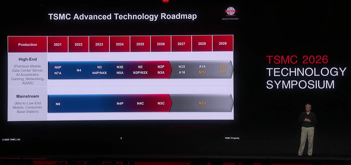
Clue Two: From A16 to A12, TSMC’s Real Pain Point Is No Longer Horizontal Scaling — It Is Vertical Integration
If High-NA is not the most urgent tool for TSMC right now, then what is the real bottleneck?
The answer is likely not that horizontal resolution is insufficient.
The real bottleneck is that vertical integration is becoming radically more difficult.
Starting with N2, TSMC is moving into first-generation nanosheet GAAFETs. A14 will extend this into a second generation, and A12 is expected to add NanoFlex Pro. That means the core challenge of the next several nodes is no longer just whether lithography can print smaller features. It is whether the full transistor architecture, materials stack, thermal budget, stress engineering, selective etching, and long-term reliability can all be solved together.

The key challenge of GAAFET is not simply a finer line.
It is a far more fragile, three-dimensional, and low-tolerance structure.
A few-nanometer-thick silicon nanosheets must alternate with SiGe sacrificial layers. During subsequent thermal processes, they must not diffuse or deform. During selective etching, the sacrificial layers must be removed without damaging the channels. After release, the nanosheets must not collapse. Every one of these steps is a process integration problem, and every integration failure can eventually show up as a catastrophic yield issue.
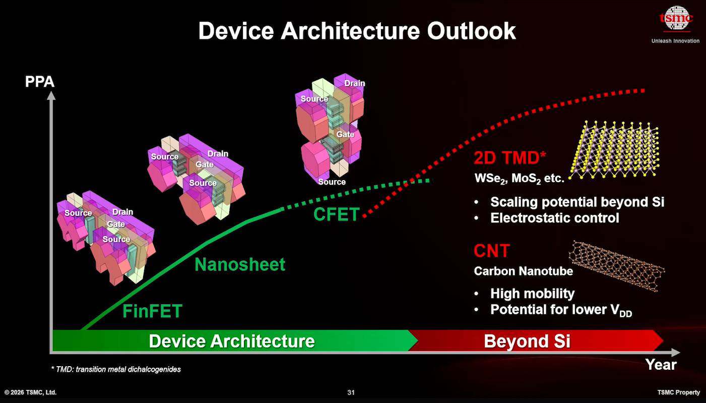
Then A16 raises the difficulty again.
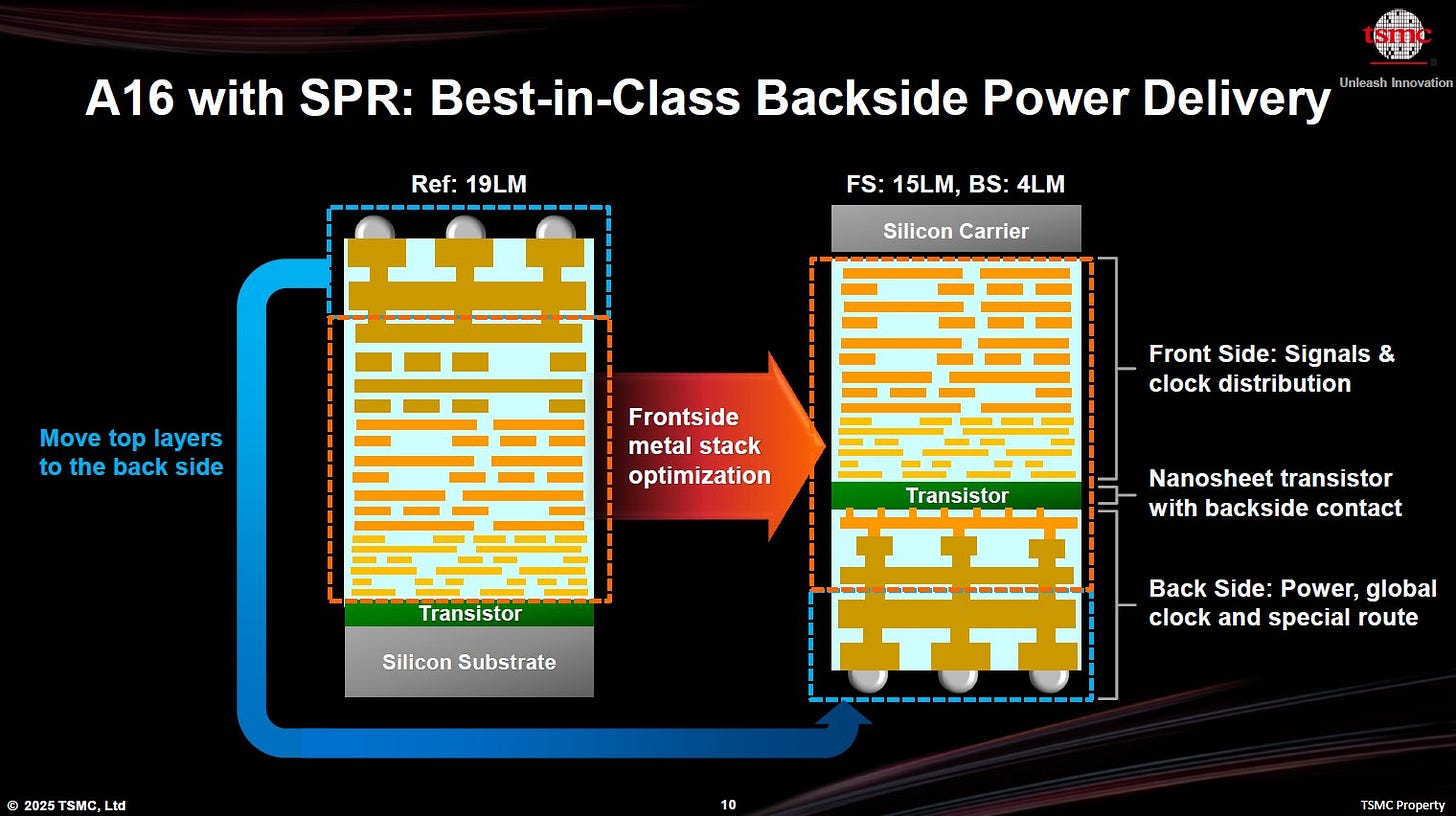
This is where TSMC will introduce Super Power Rail (SPR), moving power delivery to the backside of the wafer. This is not just another packaging-like enhancement. It fundamentally rewrites the frontside-backside integration problem. Wafer thinning, backside metallization, alignment, backside redistribution, thermal handling, and mechanical stress all become tightly linked.
And importantly, this is not a one-time transition.
Kevin Zhang made it clear that backside power delivery will continue evolving from A16 to A12.
That statement contains the real signal:
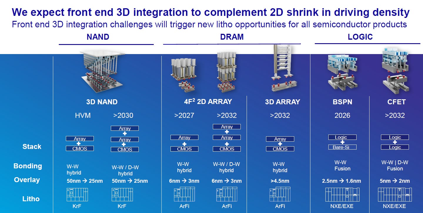
The engineering center of gravity for TSMC’s next several nodes is backside power delivery evolution and 3D integration — not simply pushing optical resolution higher.
In other words, the biggest manufacturability risk today is not whether Low-NA EUV has reached its resolution limit. It is whether the entire transistor + power delivery + BEOL + backside integration system can converge stably.
That is what makes Kevin Zhang’s comment so important.
TSMC is not saying it does not want to scale further.
It is saying that:
The dominant risk today is no longer just lithographic precision, but system-level process coordination.

2025年7月3日
Clue Three: High-NA Itself Is Still Not a Fully Mature Tool for Comfortable High-Volume Manufacturing
When the market talks about High-NA, it often focuses on its theoretical strengths: better resolution, reduced multi-patterning, and a cleaner long-term scaling roadmap.
But fabs do not buy tools for theory.
They buy them for throughput, yield, cost, and manufacturability.
And High-NA’s central dilemma is that while it offers better resolution, it also introduces a new set of major engineering penalties.
The most critical one is field size shrinkage.
To achieve a numerical aperture of 0.55, ASML’s EXE series uses anamorphic optics. The tradeoff is that the exposure field is cut roughly in half, from about 858 mm² in standard EUV to around 429 mm². For smaller mobile SoCs, this may be manageable. But for customers like Apple, NVIDIA, AMD, and Google, which regularly design large GPU, AI accelerator, and HPC dies, it becomes a very serious issue.
Many large dies simply do not fit into a single exposure field.
The consequence is stitching.
That means taking one large die, splitting it into two or more exposure regions, and then “stitching” them together. This is not a clean engineering answer. Once stitching boundaries are introduced, design rules, EDA verification, layout constraints, timing analysis, and variation control all become more complicated.
And this is not just one cost item going up.
It is a rising burden across the entire design-manufacturing-verification chain.
For AI and HPC chips, that added complexity is not a minor inconvenience. It can directly affect frequency, power, validation cycle time, and tape-out risk. For these customers, High-NA is no longer just “a better lithography tool.” It becomes a platform that may require rethinking the economics of the whole design flow.
There are additional issues as well.
First, higher source power and greater optical stress raise concerns around mirror and mask wear, tool stability, and maintenance.
Second, the next-generation larger mask ecosystem needed to better support large-die manufacturing remains delayed.
Third, the equipment is extremely expensive, which means the return on investment depends on having a very clear node strategy and customer mix.
So TSMC is not looking at a simple question of whether High-NA is technically superior.
It is asking something much more grounded:
If A13 is essentially an enhanced version of A14, and the design rules remain compatible, then if Low-NA plus multi-patterning can still solve the problem, why should the company force a transition now to a far more expensive platform whose surrounding ecosystem is still immature?
That is the key point.
High-NA’s issue today is not that it has no future.
It is that it is still some distance away from being the most efficient high-volume manufacturing tool.

What ASML Lost Is Not the Future — It Is the Sequence
This is why ASML’s stock decline should not be interpreted as the market suddenly deciding that High-NA has no value.
What the market is actually repricing is timing.
High-NA’s commercial ramp may not be ignited first by TSMC.
That is very different from saying High-NA does not matter.
For ASML, near-term revenue is still supported by Low-NA EUV volume, and AI-driven demand remains strong. What determines the next leg of its valuation multiple is whether High-NA can move into a scaling phase that lifts ASPs, margins, and the next chapter of its growth narrative.
TSMC has now told the market clearly:
At least through A16, A14, and even A13, that ignition point will not come from us.
That is meaningful. Because what ASML is losing is not necessarily order magnitude, but the validation sequence that would have come from its most influential customer moving first.
Intel, SK hynix, and Samsung will still buy.
Memory makers will still push the technology forward.
But as long as TSMC does not stand at the front of the line, the market will have a harder time fully believing that High-NA has crossed from “advanced tool” into “mainstream manufacturing platform.”
That is why the reaction was so strong.
It is not because ASML suddenly became a weaker company.
It is because its most important growth story has been delayed.
Intel’s Position Today Looks Uncomfortably Similar to Samsung’s EUV Position Seven Years Ago
If we zoom out further, this event also highlights an interesting comparison: Intel.
Today, the most aggressive logic customer pushing High-NA appears to be Intel. Combined with the roadmap around 14A and all the speculation about who may become an early adopter, Intel seems to be taking on a very specific role:
The company willing to absorb the first steep segment of the High-NA learning curve.

4月24日
That sounds bold. But it also comes with a historical warning sign: Samsung in 2019.
Back then, Samsung moved early on EUV and spoke with great confidence about technological leadership. But the real question was never whether it had the machine. The real question was whether it could bring top-tier customers into volume production, stabilize yield, and turn the technology into a scalable ecosystem advantage.
That turned out to be the hardest part.
Intel today is similar to Samsung in one sense and different in another.
The similarity is that both occupied the role of early adopter of the new lithography platform. The difference is that Intel’s current execution appears more credible than Samsung’s was at that stage. The progress of 18A at least suggests Intel is not merely selling a story.
So the real observation point is not who first declares High-NA ready today.
It is this:
By 2027, who can present verifiable high-volume yield data?
If Intel’s 14A truly turns High-NA into a commercially viable production node, then TSMC’s EXE:5000 could quickly move from an R&D evaluation tool into serious consideration for future production paths.
If yields, costs, throughput, and large-die constraints remain unresolved, then TSMC’s delay will look like an exceptionally disciplined capital allocation decision.
So this is not a story whose winner can be declared today.
But by 2027, the answer should begin to emerge.

What TSMC Is Really Refusing Is Not High-NA — It Is Paying Too Early for the Industry’s Learning Curve
If the whole story had to be reduced to one sentence, the most accurate version would not be:
TSMC has rejected High-NA.
It would be this:
TSMC has refused to pay for High-NA before High-NA proves it is the best tool for profitable high-volume manufacturing.
That distinction matters enormously.
Because what it reflects is not conservatism, but an unusually mature understanding of engineering readiness, manufacturing economics, customer structure, and technology timing.
In the earlier era of Moore’s Law, the race was defined by one question:
Who can make the transistor smaller first?
Now the race is increasingly defined by a different one:
Who can turn sufficiently advanced transistors into stable supply with the lowest risk and highest capital efficiency?
That is the new essence of advanced semiconductor manufacturing.
The most glamorous tool does not automatically win.
The most expensive path does not automatically win.
The winner is the one that makes mistakes the latest, scales the earliest, and drives yield with the highest efficiency.
TSMC’s message this time is straightforward:
From A16 through A13, it believes Low-NA remains the more efficient, more controllable, and more economically rational toolset. The truly urgent engineering battles lie in nanosheet GAAFETs, backside power delivery, process integration, and system-level manufacturability — not in rushing to extract the symbolic benefit of higher optical NA.
That is the real weight behind Kevin Zhang’s comment.
One day they may have to use it.
But not today.

4月17日
Three Real Takeaways for Investors
- ASML Is Not Broken, but Its Valuation Timeline Needs to Be Re-sequenced
Low-NA EUV remains strong, and AI demand will keep supporting shipment volume.
But if TSMC does not lead the High-NA production ramp, then the market’s assumptions about ASML’s next phase of high-margin expansion need to move further out.
This is not a story of no future.
It is a story of a future arriving later than expected.
- TSMC’s Moat Is Not Just Process Leadership — It Is Capital Discipline
Many investors think of TSMC’s advantage as purely technological. But this episode shows that one of its most powerful strengths is something else:
It knows when to invest, and when not to.
While others rush to prove they can buy the most advanced and expensive machine, TSMC is asking whether the marginal value of its current toolset has truly been exhausted.
That is not conservatism.
That is the confidence of a manufacturing leader.
- The Competitive Standard of Moore’s Law Is Being Rewritten
The future of leading-edge competition will no longer be judged only by who can reach the smallest dimensions. It will also be judged by who can deliver advanced technology at reasonable cost, at acceptable yield, and in true production scale.
That means the equipment race is not disappearing.
It is being reordered.
Resolution matters. But yield matters more.
Node naming matters. But capital efficiency matters more.
Who adopts High-NA first matters. But who turns High-NA into a replicable commercial manufacturing tool matters more.
Conclusion: By 2027, the Answer Should Start to Become Clear
So TSMC’s decision today should not be reduced to “not buying High-NA.”
More accurately, this is a strategy of timing asymmetry.
TSMC is keeping the most expensive and most symbolic tool on the R&D side for now.
It is concentrating its engineering effort on nanosheets and backside power delivery, where the immediate manufacturing risks are far greater.
And it is postponing the decisive move until others have run through the first part of the learning curve.
That is very TSMC.
It is rarely the company that rushes first.
It is the company that waits until others begin to struggle with cost, yield, and scaling — and then accelerates hard enough to redefine the standard.
So High-NA will almost certainly have its place in the future.
The real question has never beenwhetherit will be used.
The real question iswhenit becomes the most economical, most scalable, and most value-accretive production tool.
That answer is not fully visible yet.
But by 2027, as Intel 14A, memory makers’ High-NA nodes, and TSMC’s own later A-series roadmaps become more concrete, it should become much easier to tell who was investing ahead of the curve — and who was simply paying tuition too early.
TSMC’s real strength may never have been that it is first to embrace the future.
Its real strength is that it knows exactly when to embrace it — and exactly when to wait.
Thanks for reading SEMIVISION @_@! This post is public so feel free to share it.

Viewpoint from SemiVision -Deep Inisght
High-NA Timing Is Not a Delay, but a Process-Economics Decision
The market’s short-term reaction to ASML’s share price essentially reflects investors’ oversimplification of the High-NA EUV adoption timeline, rather than a deep understanding of the actual technology roadmap for advanced logic manufacturing.
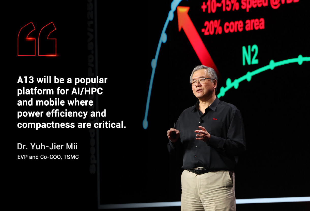
At TSMC’s latest earnings call, the company’s co-COO clearly indicated that the timing for High-NA EUV adoption may fall around the A13 node, roughly in the 2029 timeframe. From both a process engineering and economic perspective, this schedule is highly reasonable. It is also broadly consistent with mainstream industry expectations, including IBM’s view on the 1.4nm node.
The core issue is that the market often reduces EUV technology into a binary framework: Low-NA versus High-NA. In real lithography tools and process applications, however, Low-NA EUV itself is already a highly differentiated and continuously evolving product family.
Take ASML’s NXE:3800E as an example. After its introduction in 2024, improvements in source power, scanner architecture, and control systems increased wafer-per-hour, or WPH, by approximately 37.5%. This directly translates into the most critical metrics for a fab: capacity and capital efficiency. Meanwhile, the next-generation Low-NA EUV systems rumored by the market, such as the 4000F, are expected to further improve WPH and overlay performance, allowing Low-NA EUV to continue advancing not only in resolution but also in overall manufacturing productivity.
From a process perspective, WPH and overlay are not merely equipment parameters. They are core variables that determine the feasibility of multi-patterning strategies. Even in the EUV era, multi-patterning remains widely used, especially in critical layers such as FEOL gate and contact layers, as well as BEOL lower metal layers, particularly via/contact holes and cut-metal layers.
Overlay accuracy determines the alignment error between multiple exposures. This, in turn, directly affects CD control, yield, and ultimately design rules. In other words, the continuous improvement of Low-NA EUV is effectively expanding the boundary of what can be achieved within an acceptable multi-patterning cost envelope. It allows fabs to continue advancing node scaling without immediately moving to High-NA EUV.
More importantly, not every layer requires multi-patterning or extreme resolution. In actual high-volume manufacturing, many layers can still be completed with single exposure or looser design rules. This means the overall process flow is highly heterogeneous in its patterning strategy. Therefore, the value of High-NA EUV is mainly concentrated in a limited number of the most critical, resolution-constrained layers, rather than serving as a full-scale replacement for Low-NA EUV. This also explains why fabs tend to fully extract the remaining potential of Low-NA EUV before gradually introducing High-NA, instead of pursuing an aggressive technology switch.
From a cost-structure perspective, the barrier to High-NA EUV adoption comes not only from technology maturity, but also from capital expenditure pressure. A single High-NA EUV tool costs close to two or even more Low-NA EUV systems, while also bringing higher operating costs, including maintenance, mask-related adjustments, and ecosystem changes. Against this backdrop, the optimal strategy for a fab is often to maximize the productivity and depreciation benefits of existing tools, and only introduce High-NA EUV at key nodes, such as 1.4nm, when it becomes necessary to solve true resolution bottlenecks.
In summary, TSMC’s decision to delay High-NA EUV adoption is not a sign of technological backwardness or conservatism. It is a highly rational system-level choice, balancing process integration, equipment efficiency, and capital expenditure. There is also historical precedent for this approach. At the 7nm generation, TSMC extensively relied on DUV multi-patterning before gradually adopting EUV once the technology became mature enough. Today, the rapid evolution of Low-NA EUV once again makes this “delayed but not behind” strategy viable.

Low-NA EUV Can Still Be Extended Through Multi-Patterning and Process Integration
Ultimately, the adoption of High-NA EUV is not simply a question of timing. It is a question of when the technology and economics become simultaneously justified. Until then, Low-NA EUV will remain the main engine driving advanced-node scaling. Its internal generational differences and productivity improvements are the real key to understanding fab expansion and process roadmaps over the next several years.
Using ASML’s EUV platform as an example, the biggest difference between Low-NA EUV, with NA of roughly 0.33, and High-NA EUV, with NA of roughly 0.55, lies in the trade-off between resolution and depth of focus, or DOF, created by the higher numerical aperture. According to the basic relationship in optical imaging, resolution is inversely proportional to NA, while depth of focus is inversely proportional to the square of NA. Therefore, while High-NA can significantly reduce the minimum critical dimension, or CD, it also sharply compresses the process window. This greatly increases the requirements for focus control, overlay, and material flatness, which is the fundamental reason why High-NA is difficult to introduce rapidly into high-volume manufacturing.
Under these physical constraints, Low-NA EUV is not merely a transitional technology. It is a system platform that amplifies resolution through process engineering. In actual fab operations, chipmakers use multi-patterning, self-aligned patterning techniques such as SADP and SAQP, and more advanced mask design methods, including OPC and inverse lithography, to “simulate” the resolution enabled by High-NA. For example, a fine-line structure that would ideally be completed in a single exposure can be decomposed into two or even four exposure-and-etch steps. With high-precision overlay, these patterns are recombined to achieve pitch scaling close to what High-NA could provide. The core of this approach is not single-exposure capability, but the fab’s ability to control precision across the entire process integration flow.
More specifically, for Low-NA to approximate the effect of High-NA, the key lies in three dimensions. The first is overlay accuracy, which determines whether multiple exposures can be precisely aligned. The second is line-edge roughness, or LER, and CD uniformity, which ensure that accumulated errors across multiple process steps do not amplify uncontrollably. The third is controllability of process cost and cycle time. Once these three factors are optimized to a sufficient level, the final structure can still achieve similar geometric dimensions and electrical performance, even if the single-exposure resolution of Low-NA is inferior to that of High-NA.
However, this strategy of “using process engineering to compensate for optical limitations” essentially trades complexity and cost for resolution. Every additional exposure and etch step lengthens the process cycle, raises defect risk, and increases cost. As nodes continue to shrink toward the 1.4nm generation and beyond, the complexity of multi-patterning will rise nonlinearly and eventually approach its economic limit. This is when High-NA EUV begins to reveal its true value: by achieving finer pitch through single exposure, it can simplify structures that would otherwise require multiple process steps, potentially gaining an advantage in overall cost and yield.
Therefore, Low-NA and High-NA should not be viewed as direct substitutes. They are part of a staged technology relay. Low-NA pushes toward the physical limit through process integration, while High-NA provides a new optical solution once that limit can no longer be extended economically through engineering. This is why leading-edge foundries such as TSMC choose to fully extract the remaining potential of Low-NA EUV first, and only introduce High-NA at nodes where it becomes truly necessary, rather than prematurely absorbing its high cost and process risk.

High-NA Becomes Necessary Only at the Most Critical and Cost-Sensitive Layers
Placing the introduction point of High-NA EUV at A13, roughly the 1.4nm generation, is not really a “delay.” It is a precise alignment with the moment when certain geometries genuinely begin to hit the physical limits of Low-NA EUV.
Before that point, TSMC can still extract the remaining potential of Low-NA EUV, with 0.33 NA, through multi-patterning, self-aligned processes such as SADP and SAQP, and design-technology / system-technology co-optimization, or DTCO and STCO. But by A13, the issue is no longer resolution alone. Process complexity, variability, and cost begin to spiral at the same time. That is the point at which High-NA EUV, with 0.55 NA, becomes truly necessary.
From the perspective of pitch scaling, the practical single-exposure resolution limit of Low-NA EUV is roughly in the 28–30 nm pitch range. Going further requires double, triple, or even quadruple patterning. The problem is that when pitch continues to shrink toward approximately 20 nm or below, multi-patterning is no longer just a matter of “doing a few more steps.” It creates three irreversible system-level problems.
First, overlay error accumulates across multiple patterning steps and directly translates into CD variation and edge placement error, or EPE. Second, line-edge roughness, or LER, accumulates through repeated etch and deposition steps, affecting electrical performance and variability. Third, cycle time and mask count increase nonlinearly, causing the cost structure to lose economic viability. In other words, before A13, Low-NA can still be extended through engineering. But at A13, the cost of adding yet another multi-patterning step may become higher than the cost of moving to a new optical system.
Importantly, High-NA is not required for the entire chip. It is needed for a limited number of critical layers that determine transistor density and performance.
The first category is the FEOL gate stack and channel-definition layers, corresponding to GAAFET, nanosheet, forksheet, and eventually CFET structures. These layers directly determine contacted poly pitch, or CPP, and transistor density. When CPP approaches roughly 40 nm or below, Low-NA almost inevitably requires SAQP or even more advanced patterning schemes. At that point, overlay and LER become the primary constraints, and High-NA can maintain geometric precision with fewer exposure steps.
The second category is contact and via layers, especially source/drain contacts and local interconnect structures such as M0/M1 vias. These features are small in dimension but extremely large in quantity, and they are highly sensitive to overlay. Any misalignment can increase contact resistance or cause shorts. In advanced nodes, contact pitch and via pitch often approach their limits earlier than metal lines. This makes them one of the highest-value application areas for High-NA: reducing the patterning complexity and defectivity of contact/via formation through single exposure or fewer exposure steps.
The third category is the lowest BEOL metal layers, especially M0 to M2, as well as cut masks. These layers carry the densest local routing, and their pitch and linewidth typically scale together with FEOL. Cut metal, or line-cut / block-mask patterning, is particularly important. Under a Low-NA architecture, additional exposures are often required to define line-end positions, leading to a sharp increase in mask count and overlay burden. High-NA can improve line and cut precision with fewer patterning steps, significantly reducing multi-patterning demand.
By contrast, middle and upper metal layers, such as M4 and above, as well as most BEOL routing layers, have larger pitch and lower resolution requirements. They can continue using Low-NA EUV, or even DUV, for a long time. This again shows that High-NA will not comprehensively replace Low-NA. Instead, it will be introduced selectively and precisely for the most critical, densest, and most overlay-sensitive layers.
In summary, the fundamental reason for introducing High-NA only around A13 is not simply tool maturity. It is the intersection of three curves: the complexity curve of Low-NA multi-patterning, the process variability and yield-risk curve, and the overall cost curve. When these three curves simultaneously enter an unacceptable range in FEOL gate layers, contact/via layers, and lower-metal / cut-mask layers, High-NA shifts from being an option to becoming a necessity. Until then, extending Low-NA through process integration remains the more economically rational and manufacturing-compatible path.
The Cost Crossover Between CapEx and Process Complexity
From the perspective of advanced-node cost structures, the competition between High-NA and Low-NA EUV is not simply a generational replacement of lithography tools. It is fundamentally a trade-off between capital expenditure, or CapEx, and process complexity.
However, this strategy of “using process engineering to compensate for optical limitations” gradually approaches its limit as nodes continue to shrink. By the A13 generation, roughly around 1.4nm, multi-patterning is no longer just a matter of adding one or two extra process steps. Its complexity begins to grow nonlinearly. Each critical structure, such as gate, contact, via, and lower metal, may require double patterning or even quadruple patterning, leading to a significant increase in mask count. Since EUV masks are extremely expensive and difficult to fabricate, the growth in mask count can rapidly amplify total manufacturing cost. In some cases, it may even exceed tool depreciation pressure and become the dominant driver of wafer cost.
The more critical constraint comes from the cumulative effect of overlay error. In a Low-NA multi-patterning flow, each exposure and alignment step introduces small errors. After multiple layers and patterning steps, these errors accumulate into edge placement error, or EPE, directly affecting critical dimension, or CD, control and device electrical characteristics. For structures such as contacts and vias, which are extremely small and highly dense, overlay deviation can increase contact resistance or even cause opens and shorts, creating a structural impact on yield. As nodes shrink further, this error is no longer a tolerable process variation. It becomes a key bottleneck determining whether a product can enter high-volume manufacturing.
In addition, the process-step increase caused by multi-patterning significantly lengthens cycle time and further raises work-in-progress, or WIP, costs. Each additional exposure and etch step means more tool occupation, greater scheduling complexity, higher defect risk, and a higher probability of rework. In large-scale advanced-node manufacturing, these “hidden costs” often exceed the price of any single piece of equipment and have a profound impact on overall operating efficiency.
This is where the value of High-NA EUV, with 0.55 NA, begins to emerge. Although High-NA tools are significantly more expensive than Low-NA tools, and may not have an advantage in throughput, or WPH, and tool maturity during the early stage, their core advantage lies in achieving smaller geometries with fewer exposures. By reducing the need for multi-patterning, High-NA can lower mask count, simplify process flows, shorten cycle time, and improve overlay and CD control, thereby improving overall yield. In other words, High-NA is not merely about improving resolution. It is about consolidating risks and costs that were previously distributed across multiple process steps into fewer lithography steps.
Therefore, from an economic-model perspective, there is a clear cost crossover point between Low-NA and High-NA. Before nodes reach the extreme scaling regime, the cost of extending Low-NA through process engineering remains lower than the investment required for High-NA tools. However, once multi-patterning complexity, overlay error, and cycle-time costs simultaneously rise beyond a critical threshold, High-NA becomes the more economically rational choice. This crossover point is the fundamental reason why a foundry such as TSMC would choose to introduce High-NA only around A13.
Overall, the Low-NA EUV strategy is to maximize existing optical capability through process engineering, while the High-NA EUV strategy is to simplify process engineering by upgrading optical capability. The two are not direct substitutes. They are optimal solutions for different stages of node scaling. Once the marginal cost of process complexity exceeds the marginal cost of additional lithography capital, the technology path will naturally shift toward High-NA. A13 is most likely where this inflection point begins to appear.

Thanks for reading SEMIVISION @_@! This post is public so feel free to share it.


PreviousNext