Samsung’s Next AI Bet: CPO Platforms and LPU Foundry
Samsung’s Next AI Bet: CPO Platforms and LPU Foundry
- Source: SemiVision
- Author: SEMIVISION
- Published: 2026-04-25T17:33:52+08:00
- URL: https://tspasemiconductor.substack.com/p/samsungs-next-ai-bet-cpo-platforms (1) Samsung’s Next AI Bet: CPO Platforms and LPU Foundry


Samsung’s Next AI Bet: CPO Platforms and LPU Foundry
Original Article By SemiVision Research [Reading time: 30 mins]

Apr 25, 2026
∙ Paid
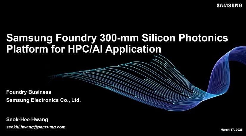
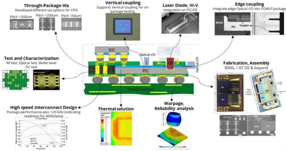
Samsung Electronics has been actively developing its 300mm silicon photonics platform in recent years to address the surging demand for data center interconnects driven by AI and HPC computing. First unveiled at OFC 2026, the company’s 300mm silicon photonics platform is built on a mature CMOS process and incorporates features such as a 305 nm silicon layer, a 400 nm silicon nitride layer, PN-doped modulators, germanium waveguide photodiodes, thermo-optic phase shifters, TSVs, and bump packaging. The platform delivers low-loss silicon/SiN waveguides and broadband coupling efficiency, high-speed microring and MZM modulators exceeding 50 GHz, as well as high-speed and avalanche photodetectors operating at 50 GHz and 20 GHz. Its accompanying PDK supports more than 40 component models, provides full DRC/LVS/PEX verification, and takes into account factors such as free-carrier absorption and self-heating effects, improving consistency between simulation results and actual wafer performance.

2025年6月21日

2025年6月8日
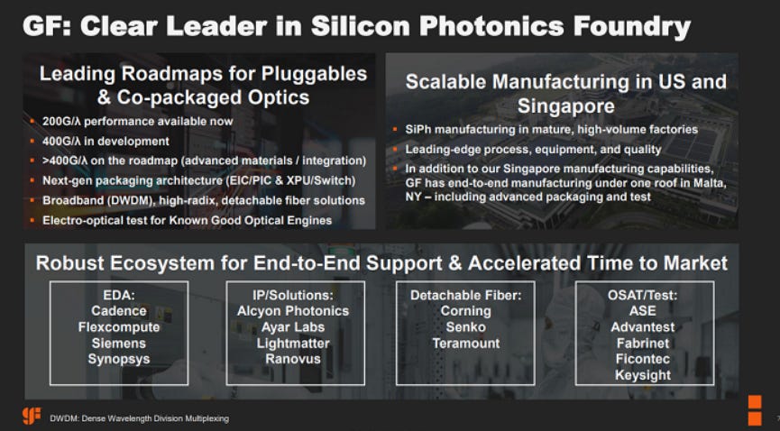
From an industry competition standpoint, TSMC currently holds a leading position in silicon photonics. Its COUPE (COmpact Universal Photonic Engine) platform has already been presented publicly at the Global Silicon Photonics Summit, and the company is targeting mass production of co-packaged optics (CPO) solutions in 2026. Intel, meanwhile, continues to invest heavily in silicon photonics and on-chip optical I/O. In comparison, Samsung and GlobalFoundries are aggressively catching up: Samsung is focused on AI data center applications, while GF has become the largest pure-play silicon photonics foundry supplier through its acquisition of Singapore-based AMF.
Source: A*STAR
In Singapore, the government has long invested in photonics R&D. ASTAR IME has established a silicon photonics research base and, in 2024, took the lead in forming the Photonics Chiplet Consortium to integrate advanced packaging and heterogeneous integration technologies. GF is working closely with ASTAR and plans to establish a silicon photonics Center of Excellence in Singapore, linking together semiconductor industry, academic, and research resources. Taken together, silicon photonics technology and its ecosystem are rapidly maturing around the demands of AI and HPC, and Samsung’s launch of a full commercial-grade platform comes at a highly strategic moment.
A*STAR And Globalfoundries Collaborate To Further Research In Silicon Photonics For AI Era
Technical Highlights
For active devices, the platform incorporates multiple structures. Multi-step doping is used to form PN junctions as the basis for microring modulators (MRMs), Mach–Zehnder modulators (MZMs), and photodiodes. Selective germanium epitaxy is used to fabricate high-gain avalanche photodiodes (APDs) and waveguide-based high-speed photodetectors (HSPDs). It also integrates Ge-based thermo-optic phase shifters through bonding and adds metal-insulator-metal (MIM) capacitors in the backend to strengthen power integrity. On the advanced packaging side, the platform supports through-silicon vias (TSVs) and bump technologies, enabling high-speed interconnection with external electronic ICs (EICs), interposers, and related components.
The platform is also supported by a complete design environment and PDK. It provides more than 40 device models for circuit simulation in commonly used electronic design automation (EDA) tools, along with standard DRC, LVS, layout-versus-schematic checks, and parasitic extraction (PEX) verification flows. Advanced models account for free-carrier absorption, thermal effects, and wavelength-dependent electro-optic response, allowing simulation results, such as 50 Gbaud PAM4 eye diagrams, to closely match measured hardware performance.
Strategy and Partnerships
Samsung positions silicon photonics as a key differentiating weapon in future AI/HPC semiconductor competition. Its semiconductor device division has recently launched a major recruitment effort for silicon photonics talent in Singapore, establishing a dedicated R&D center led by King-Jien Chui, a former senior TSMC executive. Industry reports indicate that Samsung has identified silicon photonics as a strategic investment priority and is collaborating with optical communications giant Broadcom to commercialize the technology. According to industry sources, Samsung is targeting the launch of a commercial CPO solution in 2027 and believes it will begin direct competition with TSMC from that point onward. This suggests that Samsung sees silicon photonics as a key enabler for attracting data center customers.
At the same time, other international players are moving aggressively. In November 2025, GlobalFoundries (GF) acquired Singapore-based silicon photonics foundry AMF, integrating manufacturing capability and IP, and thereby becoming what it describes as “the world’s largest pure-play silicon photonics foundry.” GF has stated that it will combine AMF’s 200mm platform technology and gradually transition toward 300mm, while planning capacity expansions in both the United States and Singapore to meet AI data center demand. On the R&D side, GF will work with Singapore’s A*STAR IME to establish a local silicon photonics Center of Excellence focused on high-speed materials and device research above 400 Gbps. The industry widely believes that while TSMC currently leads, the moves by Samsung and GF will reshape the silicon photonics ecosystem and push optical interconnects to the forefront of foundry competition.
Singapore-Related Developments
Samsung in Singapore:Samsung has already established a silicon photonics R&D center in Singapore and is aggressively recruiting photonics specialists. The new team is led by King-Jien Chui, who previously held a senior role at TSMC and brings extensive experience in optical interconnects. Reports indicate that Samsung is expanding its R&D headcount in Singapore and is working with Broadcom to develop silicon photonics modules and systems in order to accelerate commercialization.
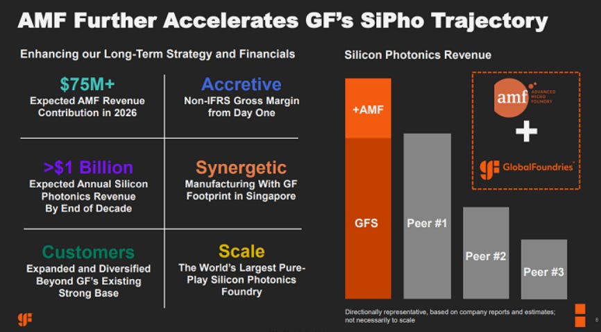
The deal significantly strengthens GF’s silicon photonics technology portfolio and manufacturing capability, making it a leader in the silicon photonics wafer foundry market. Following the acquisition, GF will establish a Silicon Photonics Center of Excellence in Singapore and collaborate with the Agency for Science, Technology and Research (A*STAR) to conduct R&D on materials and technologies for optical interconnects above 400 Gbps. This signals that Singapore is becoming a critical global hub for silicon photonics innovation.
A*STAR and Industry Alliances:The Singapore government is actively supporting photonics technology through ASTAR IME. For example, ASTAR has taken the lead in establishing the Photonics Chiplet Consortium (CHIPLETS), focused on advanced packaging and photonic chip integration. The consortium brings together international companies and research institutions to address packaging and connectivity challenges between photonic and electronic chips. These coordinated government-industry initiatives demonstrate that Singapore is building a full photonics ecosystem spanning from research to manufacturing. The moves by Samsung and GF are highly aligned with Singapore’s strategy: Samsung can leverage local talent and research resources to accelerate development, while GF can tap Singapore’s strong silicon photonics infrastructure and talent network to strengthen its competitiveness.
Below we will share:
Samsung CPO Impact Assessment
Samsung CPO Conclusion and Recommendations
Samsung CPO Unresolved Questions and Areas to Watch
The Real Signal from GTC 2026: Why Did Nvidia Put the Groq 3 LPU on Samsung Foundry?
Why does the LPU matter? Because AI’s bottleneck is shifting from training to inference latency
Why Samsung? Because this chip lands right in Samsung’s sweet spot
What advanced packaging was used? What can be confirmed so far is that it does not look like the traditional HBM GPU playbook
This is precisely where Samsung’s opening lies: not by colliding head-on with the most crowded CoWoS/HBM battlefield.
From SemiVision’s perspective, this reveals at least three industry conclusions

4月8日
Impact Assessment
Samsung’s new platform carries multiple implications for the industry. From a technology perspective, its 300mm process and mature packaging support are expected to significantly reduce the cost of silicon photonics products while improving mass-production yield, helping accelerate the commercialization of optical interconnect devices. Compared with the current industry landscape, Samsung’s platform covers low-loss waveguides, broadband couplers, and high-speed modulators/detectors, placing it on the same competitive tier as TSMC’s COUPE and Intel’s photonics technologies. In particular, Samsung has already provided comprehensive design support through its PDK. Reportedly, TSMC’s COUPE is also equipped with a full PDK covering waveguides, splitters, WDM, and more. Going forward, both platforms are expected to support advanced packaging technologies such as silicon interconnects (TSVs, Cu + micro-bumps) to enable heterogeneous integration through bumping and hybrid bonding. At present, their development directions are clearly converging.

2025年3月28日

Samsung has already established partnerships with major optical communications players such as Broadcom, and it can leverage its strengths in memory and logic co-packaging to offer one-stop solutions that are highly attractive to data center customers. The maturity of Singapore’s ecosystem also provides a strong R&D and talent advantage, which Samsung should use to accelerate technology iteration.
Overall, Samsung’s silicon photonics platform strengthens its competitiveness in AI data center optical interconnects. However, the market battle is already fully underway: TSMC’s CPO/photonics strategy, GF’s pure-play foundry positioning, and Intel’s advanced packaging roadmap all represent serious competition. Looking ahead, Samsung will need to focus on customer-oriented solutions and make full use of its global R&D network to accelerate upstream and downstream collaboration, thereby reinforcing its position within the ecosystem.

3月2日
Conclusion and Recommendations
Samsung Foundry’s 300mm silicon photonics platform has already demonstrated impressive technological completeness, including low-loss waveguides, high-speed components, and a full PDK, making it well aligned with the bandwidth and energy-efficiency demands of AI/HPC data centers.
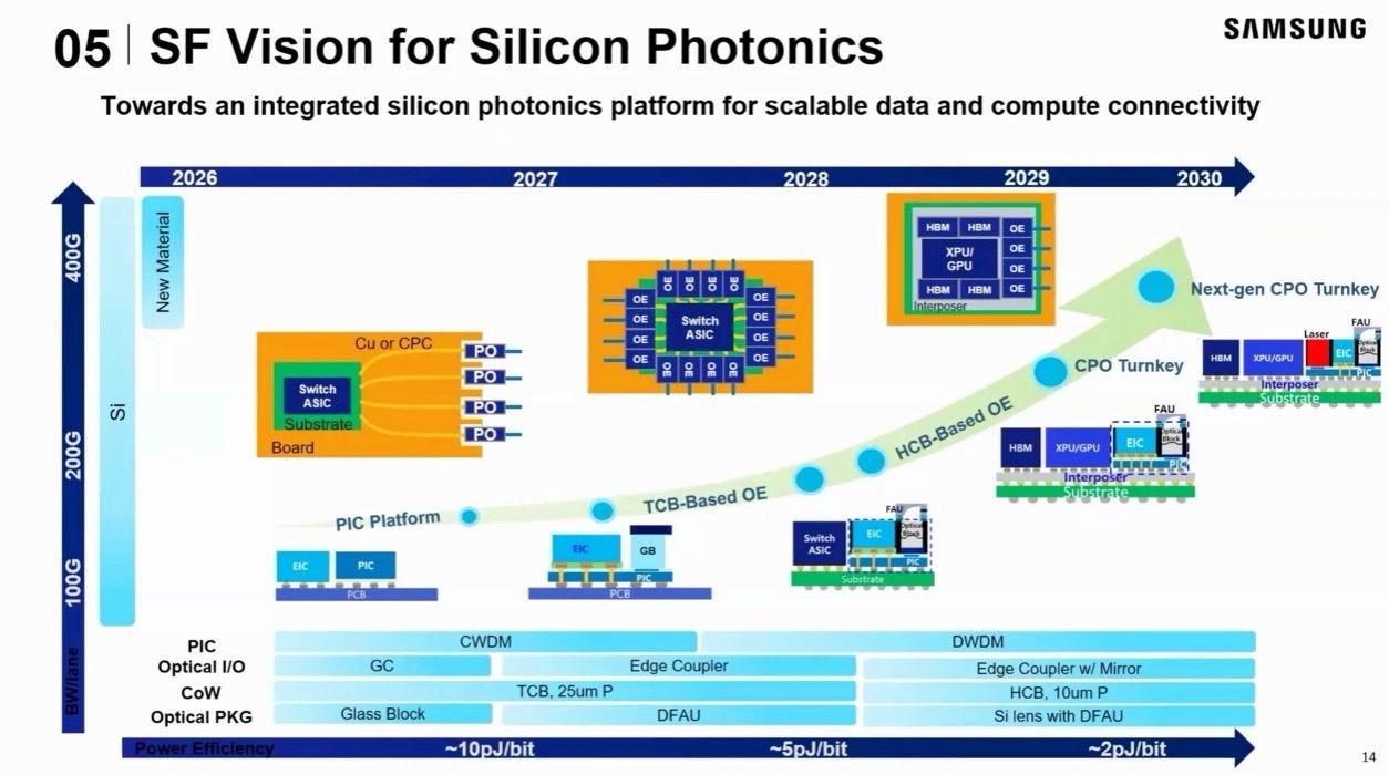
To accelerate practical deployment, Samsung is advised to further advance the following strategies:
Accelerate mass production and manufacturing readiness:
Move forward with volume production of 300mm silicon photonics wafers, including expansion into the C-band, continued yield improvement in mature processes, and closer collaboration with packaging houses to improve testing and die-singulation workflows.
Strengthen ecosystem collaboration:
Work more deeply with equipment vendors and system companies, such as Broadcom and Cisco, at both the silicon photonics module and system levels to ensure Samsung’s components can be smoothly integrated into existing data center network architectures.
Leverage the Singapore R&D center:
Use Singapore’s strong R&D and educational resources to accelerate device development and talent cultivation. Samsung could also consider joint development programs with A*STAR IME and its partners, such as Raytheon and Applied Materials.
Define global market positioning:
Capitalize on Samsung Foundry’s global supply chain advantages to target AI and optical communications customers with real mass-production demand, and offer customized silicon photonics services that highlight Samsung’s differentiation versus TSMC and GF, such as tight co-packaging integration with memory.
Overall, silicon photonics is rapidly moving from the laboratory into a wave of commercialization. Samsung should seize this opportunity by leveraging its semiconductor integration and manufacturing capabilities, while coordinating innovation with global R&D resources, in order to establish a leadership position in next-generation optical interconnects.
Unresolved Questions and Areas to Watch
Mass-production timeline and process roadmap:
When will Samsung begin production, and to which future process nodes does it plan to extend the platform?
Support for the C-band or other optical communication bands:
The current discussion mainly refers to the O-band. How will Samsung address C-band applications?
Potential collaboration with more system makers or hyperscale data center operators:
When might the first commercial silicon photonics products or sample deliveries emerge?
Specific co-packaged optics application cases:
How does Samsung plan to combine this platform with its latest SoC and HBM packaging technologies to realize optical I/O?
Operating model of the Singapore R&D center:
Beyond partnership announcements, how will Samsung further integrate R&D and manufacturing efforts in Singapore?
These questions should serve as key points for continued observation when evaluating Samsung’s progress and execution in the silicon photonics market.
3月26日
The Real Signal from GTC 2026: Why Did Nvidia Put the Groq 3 LPU on Samsung Foundry?
What mattered most at GTC 2026 was not just Vera Rubin, Rubin Ultra, or even NVIDIA once again framing AI infrastructure as a complete system spanning chips, networking, memory, and the entire AI Factory. The more intriguing signal was Jensen Huang explicitly naming Samsung on stage as the manufacturing partner for the new-generation Groq 3 LPU. This was not merely a supplier acknowledgment. It was a sign that the division of labor in the AI chip industry is being rewritten. In Samsung’s own GTC 2026 technical post, the company also confirmed that Jensen specifically mentioned Samsung as the manufacturing partner for Groq’s new-generation LPU, indicating that the relationship between the two companies has expanded from memory into the more strategic realm of logic foundry.

If this is interpreted simply as “Samsung finally won an NVIDIA order,” that is too shallow a reading. A more accurate interpretation is that NVIDIA is reconfiguring the AI chip supply chain in a much more sophisticated way. The most critical training GPUs — those that consume the greatest share of HBM and 2.5D advanced packaging resources — still remain within the existing high-barrier supply chain structure. But on the other major front that is now emerging in the inference era — dedicated inference accelerators designed for low latency, high data reuse, and agentic AI workloads — a different combination of foundry and packaging is beginning to appear. The Groq 3 LPU is one of the clearest representatives of this new path.
Why does the LPU matter? Because AI’s bottleneck is shifting from training to inference latency
The core concept behind Groq’s LPU is not to build “another kind of GPU,” but to redesign the processor specifically for large-model inference. Groq’s own definition of the LPU is very clear: it is a new type of processor built from the ground up for AI inference, optimized for speed, latency, cost, and energy efficiency, rather than for the broad workload coverage that traditional GPUs aim to provide. By GTC 2026, the Groq 3 LPU had been formally incorporated into NVIDIA’s platform narrative, which further suggests that NVIDIA itself now accepts a key reality: future AI data centers will not consist of GPUs alone. They will also include dedicated inference co-processors with clearly differentiated roles.
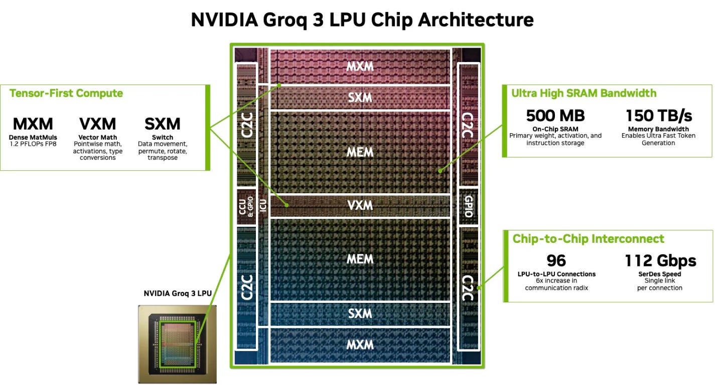
Based on public information, the most striking feature of the Groq 3 LPU is its 500MB of on-chip SRAM and 150TB/s of bandwidth. The strategic significance behind those numbers is not simply how large the memory is, but what it represents: data is kept on-chip and reused as much as possible, rather than being constantly moved back and forth to external memory. For large language models — especially in decode, real-time interaction, and multi-agent coordination scenarios — the cost of data movement is rapidly becoming the next major bottleneck. As inference demand shifts from merely “being able to run” to requiring real-time performance, stability, and low latency, the value of large on-chip SRAM will be fundamentally repriced.

3月17日
Why Samsung? Because this chip lands right in Samsung’s sweet spot
The process information currently available points to the Groq 3 LPU being built on Samsung Foundry’s SF4X, part of its 4nm family. According to Samsung’s official materials, SF4X is the most heavily optimized version within its 4nm family for HPC, featuring higher-drive transistors and improved back-end-of-line (BEOL) interconnects to reduce RC delay, with the explicit goal of supporting high-performance computing. In other words, this is not a node lightly tuned for smartphone SoCs. It is Samsung’s dedicated FinFET-era offering for competing in HPC and AI chips.

The key point here is that the design logic of the Groq 3 LPU differs from that of a traditional large GPU. It is not chasing maximum general-purpose compute, ultra-high HBM bandwidth, or deep dependence on the most mature 2.5D packaging ecosystem used for large training chips. Instead, it is optimized around bandwidth, latency, determinism, and overall efficiency under a large-SRAM architecture. That makes 4nm, rather than 3nm or 2nm, a more rational engineering choice: it offers a better balance among power, yield, die area, design risk, and cost. For Samsung, this type of product is better suited than a top-tier training GPU as an entry point into the AI logic foundry market. For NVIDIA, it provides a way to establish a second advanced AI chip manufacturing path without disrupting its existing primary supply chain.

2月13日
What advanced packaging was used? What can be confirmed so far is that it doesnotlook like the traditional HBM GPU playbook
When it comes to packaging, the easiest mistake the market can make is to see Samsung’s advanced packaging capabilities and immediately assume that the Groq 3 must be using I-Cube or X-Cube. At this point, there is no public official evidence for that claim. Samsung does indeed emphasize its advanced packaging capabilities and continues to promote platforms such as I-Cube, H-Cube, and 3D packaging. But so far, there is no publicly available document that directly identifies which Samsung packaging brand, if any, is being used for the Groq 3 LPU.
That said, the public information already gives us enough evidence to rule out certain possibilities. Samsung’s definition of I-Cube is very clear: it is a 2.5D heterogeneous integration solution that horizontally integrates one or more logic dies with multiple HBM stacks on an interposer. Samsung’s official description of I-Cube4 is even more explicit: it consists of “four HBM stacks plus one logic die” placed on a silicon interposer. That kind of package is typically used for GPU-plus-HBM configurations.
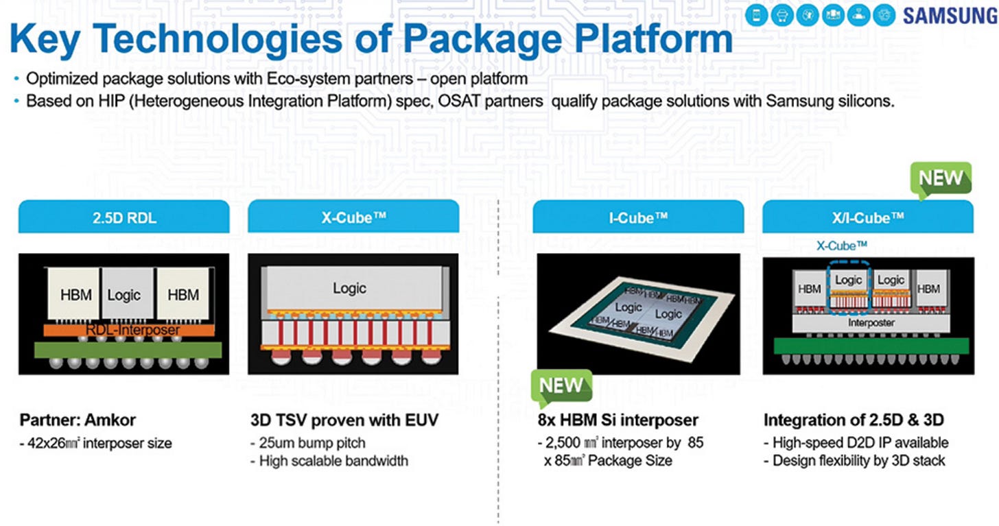
The public narrative around the Groq 3 LPU, however, points in the opposite direction. Its core selling point is 500MB of large on-chip SRAM, not external HBM. That means its system-level value comes from building the high-bandwidth data path directly into the chip as much as possible, rather than relying on HBM stacks and a 2.5D interposer to solve the bandwidth problem. Based on the evidence currently available, the Groq 3 is therefore unlikely to follow the standard I-Cube or CoWoS route of “logic + HBM + silicon interposer.” Instead, it looks more like a high-performance monolithic die paired with high-end packaging, thermal design, and system-level interconnect optimization. In other words, what can be confirmed today is notwhichSamsung packaging brand it uses, but rather that it appears to have been deliberately designed to avoid the most capacity-constrained HBM 2.5D packaging route.


This is precisely where Samsung’s opening lies:not by colliding head-on with the most crowded CoWoS/HBM battlefield.
Over the past two years, what AI chips have truly been short of has never been wafer starts alone, but rather HBM supply and advanced packaging capacity. Whoever can secure more HBM, and whoever can reserve more 2.5D interposer and advanced packaging lines, can ship more high-end AI GPUs. That is why most market discussion has revolved around CoWoS, I-Cube, HBM3E, and HBM4.
But the Groq 3 LPU offers a different answer: not every inference chip has to take the most crowded route of “big GPU + big HBM + large interposer.
”If certain inference scenarios care more about token latency, deterministic execution, decode efficiency, and energy efficiency, then using large amounts of SRAM in exchange for extremely high on-chip bandwidth can, to a considerable extent, bypass the HBM bottleneck. For Samsung, this is a smarter path than confronting TSMC directly in the highest-end AI training GPU segment. For NVIDIA, it creates a second supply chain for inference infrastructure and reduces dependence on a single route.
At the same time, the Nvidia Groq LPX also uses DDR DRAM, not just SRAM. It does not replace HBM; instead, it actually increases DDR DRAM demand.
One of the focal points at GTC was the Groq LPU and LPX rack. Because they are often highlighted for their use of SRAM, some people may mistakenly assume they do not require DRAM.
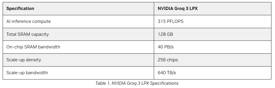
- The LPU uses SRAM, but it does not replace HBM or DRAM
The LPU is designed to share and accelerate part of Rubin GPU’s workload—specifically, the FFN/MoE portion of inference decode, not the attention portion. It isnotreplacing Rubin, which still relies on HBM.
- An LPX Compute Tray contains more than just LPUs
Eight LPUs form one LPX Compute Tray (a server node). But this tray does not consist only of LPUs; it also includes one CPU. And any CPU necessarily requires DRAM. Then, 32 LPX Compute Trays are combined into one LPX rack with a total of 256 LPUs.

For comparison, an Nvidia HGX NVL8 server uses an x86 CPU (or Vera in the future), equipped with 1 TB to 2 TB to 4 TB of DRAM, while the UBB carries eight Hopper or Blackwell GPUs equipped with HBM as accelerators. In the same way, one Groq 3 LPX Compute Tray includes one CPU, likely an x86 CPU, with RDIMM DDR DRAM, plus eight LPU accelerators. In that sense, the LPU/SRAM combination plays the same role as Hopper/HBM: it serves as the AI accelerator plus VRAM layer, while the separate x86 CPU + DRAM runs the operating system and main program.
- How much DRAM is on an LPX Compute Tray?
Based on two clues, the estimate is 384 GB of DDR5 DRAM.
(1)On page 11 of Micron’s earnings presentation, the last bullet says one Nvidia Groq 3 LPX rack has up to 12 TB of DDR5 DRAM.
12 TB / 32 trays = roughly 375 GB per tray. Since 12 TB is a rounded number and there are slight differences between decimal and binary calculations, the actual figure could reasonably be around 384 GB.
(2)In the LPX Compute Tray photo released by Nvidia, there is one host CPU. If there is a CPU, there must also be DRAM. Looking at the photo, it appears there are either 4 or 6 RDIMM slots, suggesting something like 64 GB × 6 = 384 GB or 96 GB × 4 = 384 GB.
- What kind of CPU is being used?
Because Micron’s slide specifically says DDR5, it is likely an x86 CPU. Nvidia’s own Grace and Vera use LPDDR5X, not DDR5, and their capacity figures do not match either. Grace is 480/512 GB, while Vera is 1.5 TB, both too large relative to the roughly 375 GB-per-tray range implied here.
- There is also a BlueField-4 DPU on the LPX Compute Tray
That DPU reportedly includes 128 GB of onboard LPDDR5X, which is not included in the 384 GB estimate above. If included, the total DRAM amount would be even higher.
- The conclusion: LPU on-chip SRAM does not replace Rubin’s HBM
Instead, the LPX tray and rack increase total DDR DRAM usage, meaning the overall effect is actually higher DRAM demand, not lower.
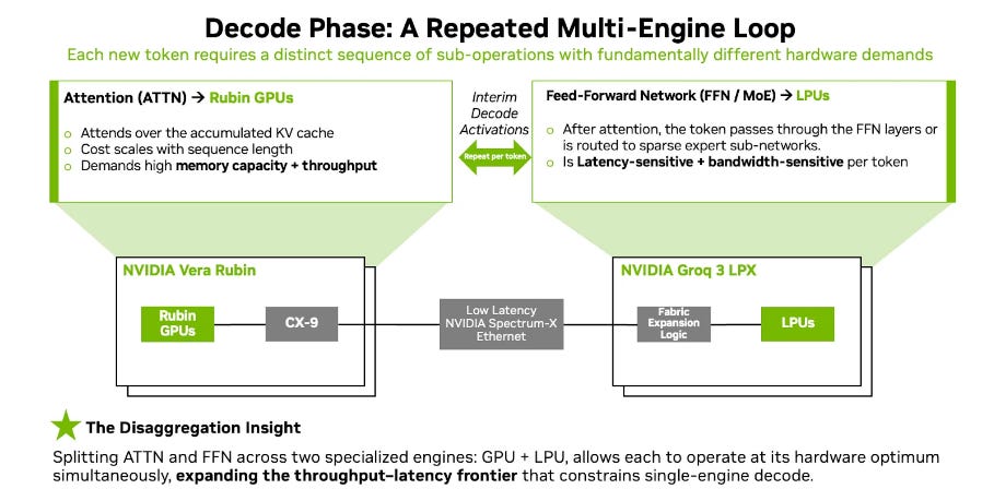
It now seems many people may have guessed wrong. The Groq LPU is not acting as the standalone decoder in disaggregated inference. In fact, both prefill and decode are still handled by the Rubin GPU. Decode is then further split into Attention and FFN/MoE—what Nvidia calls AFD (Attention-FFN Disaggregation). The FFN/MoE portion is specifically assigned to the LPU. In other words, the LPU is effectively an outsourced subcontractor for part of Rubin GPU’s decode workload.
Indisaggregated inference (P/D inference):
-
Prefill is compute-intensive: Rubin GPU
-
Decode is memory-bandwidth-intensive: Rubin GPU
Then part 2 is further split via AFD (Attention-FFN Disaggregation).
In LLM decode, every layer must go through both Attention and FFN/MoE stages. If the model has 100 layers, that cycle happens 100 times. Attention requires large memory capacity, and the LPU’s SRAM capacity is too small for that—around 500 MB per LPU, and even an entire LPX rack only has about 128 GB of SRAM, which is far too small to hold the weights of a very large LLM. That is why attention still stays on Rubin GPU, with its 288 GB of HBM4.
By contrast, the FFN stage in dense models, or the routing and execution of selected experts in MoE models, requires extremely frequent memory access and is highly bandwidth-intensive. That makes it a much better fit for LPU SRAM.
So there are effectively three roles:
Prefill:Rubin GPU chips / VR NVL72 racks
Decode-Attention:Rubin GPU chips / VR NVL72 racks
Decode-FFN/MoE:Groq 3 LPU chips / Groq 3 LPX 256 racks
Roles (2) and (3) loop back and forth many times.
The number of chips, trays, or racks used for (1), (2), and (3) can be configured flexibly based on the actual inference workload. You can scale by chip count, tray count, rack count, or cluster count.
Communication between (1) and (2) for KV cache can use NVLink scale-up within the same NVLink domain, or RDMA Ethernet for scale-out, such as Spectrum-X. Once the number of GPUs becomes large enough to span multiple racks or separate prefill and decode clusters, Ethernet becomes the only practical option.
Communication between (2) and (3) for interim decode activations currently can only use scale-out RDMA Ethernet or InfiniBand, because the LPU has not yet been integrated into NVLink in time. In the future, Nvidia may allow each LPU in an LPX rack to communicate over NVLink.
There is no direct communication needed between (1) and (3), because role (3) is essentially an outsourced extension of role (2).
Beyond serving as Decode-FFN/MoE in AFD, another recent theory is that an LLM can embed a small internal model to predict decoding for a short span, and then let the main LLM verify the result, thereby increasing speed. The LPU/LPX architecture is also well suited to running these smaller predictive decode models. For example, in highly predictable content such as Tang poetry, classical prose, or Shakespearean passages, a much smaller model may be able to generate a short sequence without invoking the full multi-trillion-parameter LLM token by token. The internal small model predicts a short span of tokens, the LLM verifies the result, and if correct, the small model continues generating.
The broader conclusion is that Nvidia is moving incredibly fast. Many of these ideas are only beginning to move from the research-paper stage toward broader adoption, yet Nvidia already has products in place. When you think about how Google’s latest TPU v7 Ironwood still does not support native hardware FP4 quantization, Nvidia’s product roadmap appears nearly two years ahead on certain specifications—even though Google remains one of the industry’s leading producers of frontier AI models and papers.

3月30日
LPX is deployed alongside Vera Rubin NVL72 to accelerate the latency-sensitive portions of the decode loop, including FFN execution and MoE expert execution, while Rubin GPUs continue to handle prefill and decode attention. Together, the two create a heterogeneous service path that improves interactive responsiveness without sacrificing AI factory throughput.

At the core of LPX is the NVIDIA Groq 3 LPU, which is designed to deliver fast and predictable token generation through the tight coupling of compute, memory, and communication under compiler control. The LPU architecture is built around this same principle: tightly coupling compute, memory, and communication to enable fast and predictable token generation under compiler control. The LPU is optimized not only for peak arithmetic throughput, but also for deterministic execution, high on-chip memory bandwidth, and explicit data movement. These capabilities are especially important for decode-heavy, latency-sensitive inference systems. ... The LPU is built on Groq’s spatial execution model, in which the compiler explicitly schedules computation, data movement, and synchronization. Rather than relying on a runtime dynamic hardware scheduler, the compiler depends on a quasi-synchronous inter-chip protocol implemented in hardware, eliminating natural clock drift and aligning hundreds of LPU accelerators to operate as a single coordinated system. With predictable data arrival and regular software synchronization, developers can reason about timing more directly, and the system can coordinate computation and network behavior in a more explicitly deterministic way.
Systems optimized for maximum aggregate throughput are not always the best fit for workloads that require fast and predictable token generation for each request.
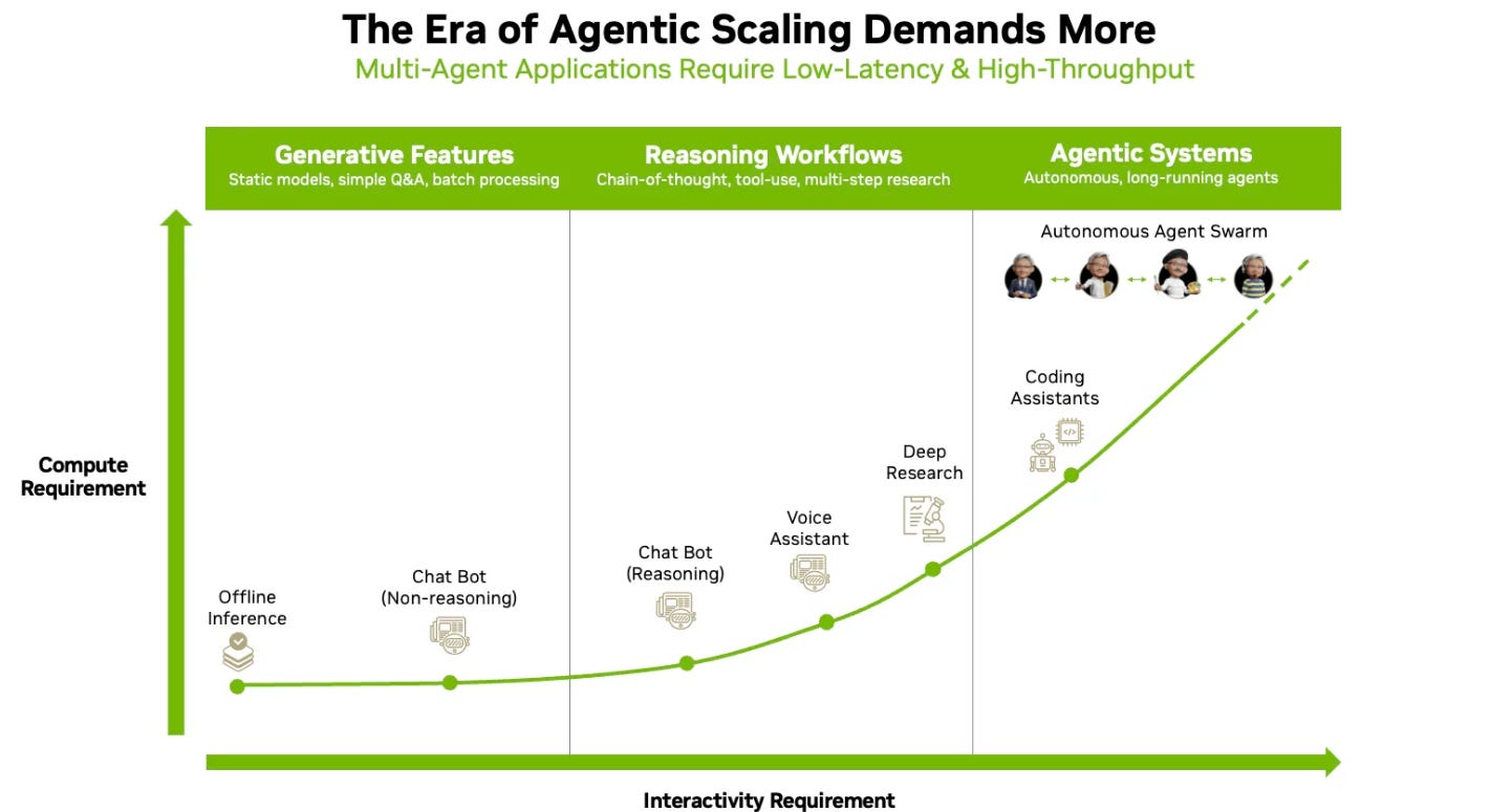
In agentic AI, this challenge becomes even more pronounced, as the system is constantly cycling through reasoning, retrieval, tool use, and further reasoning. In these loops, latency accumulates at every step, making stable per-token performance and strong tail-latency behavior essential for a responsive user experience.
Rubin GPUs are the flexible, general-purpose workhorses for both training and inference. They deliver high throughput across a wide range of model sizes, batch structures, and serving modes, from long-context prefill to decode attention and large-scale, high-concurrency inference.
LPX adds a dedicated path optimized for fast and latency-sensitive token generation. Together, they enable a heterogeneous inference design that improves interactive responsiveness without sacrificing system-scale efficiency.
The prefill stage is mainly about ingesting large inputs and building the KV cache—this workload benefits from dense parallel compute and large memory capacity. Vera Rubin NVL72 handles this stage effectively, especially for long-context workloads and mixture-of-experts (MoE) models, where context can be both large and highly variable.
The decode stage is different. Decode is a per-token repeated loop, and different parts of that loop create different bottlenecks. In the Vera Rubin platform architecture, LPX is best understood as part of a dual-engine decode loop. The GPU handles the parts of decode that benefit most from throughput and large memory capacity, such as full-context attention over the accumulated KV cache. LPX accelerates the latency-sensitive execution within decode, such as sparse MoE expert feed-forward networks (FFN) and other pointwise operations. This separation is often referred to as decode-phase disaggregation or attention-FFN disaggregation (AFD), which separates attention and FFN during decode and exchanges intermediate activations for each token step, allowing each engine to execute the portion of the loop it is best suited for. This AFD loop extends the Pareto frontier for the highest-value operating region. At rack scale and above, LPX is designed as a highly coordinated compute unit that reduces coordination overhead and minimizes jitter. This is especially valuable in decode-heavy, agentic workflows, where small latencies accumulate across many model calls and verification loops.

In practice, Dynamo routes prefill to GPU workers to handle large contexts and build the KV cache. During decode, Dynamo orchestrates the AFD loop: the GPU performs attention over the accumulated KV cache, intermediate activations are then sent to the LPU for FFN/MoE execution, and the outputs are returned to the GPU to continue token generation. The result is a single coherent serving path with more predictable tail latency while maintaining high AI factory throughput. Through KV-aware routing, low-overhead transfer, and latency-targeted scheduling, Dynamo helps interactive sessions avoid long queues, reduces cross-tenant jitter, and maintains stable tail latency even as concurrency and request shapes vary. The end result is a production-ready heterogeneous serving model that can deliver responsive user experience at scale while preserving high AI factory throughput.
Speculative decoding is becoming an increasingly important technique for reducing large language model inference latency. This method uses a smaller draft model to generate multiple candidate tokens in advance, while a larger target model verifies and accepts those tokens in parallel. When the predictions align, multiple tokens can be committed at once, significantly increasing effective tokens per second and reducing response latency.
LPX is highly well suited to serve as the draft-generation engine in this architecture. The LPU’s deterministic execution model and extremely high on-chip SRAM bandwidth allow draft tokens to be generated very quickly, enabling the draft model to run ahead of the verifier. At the same time, GPUs such as Rubin remain highly efficient for large-model execution tasks such as prefill, attention processing, and token verification.”

4月21日
From SemiVision’s perspective, this reveals at least three industry conclusions
First, functional specialization in AI chips is accelerating.
The future market will not be defined by a single race of “whose GPU is bigger.” Instead, it will evolve into a fully system-level division of labor across training, prefill, decode, agent orchestration, networking, and memory hierarchy. The fact that Groq 3 LPU has now been formally incorporated into NVIDIA’s platform narrative is itself a strong signal.
Second, the strategic importance of SRAM is rising.
Although its capacity is far smaller than HBM, the value of on-chip SRAM data reuse is becoming a new strategic weapon in certain inference workloads. This will affect not only chip design, but also process-node selection, tolerance for die size, power allocation, and packaging architecture.
Third, Samsung’s point of entry is not to comprehensively replace TSMC, but to first open a gap in inference-specific chips.
The significance of Groq 3 LPU being built on SF4X is not whether “4nm is advanced enough,” but that it marks Samsung finally securing a position in AI logic foundry that is both symbolic and commercially scalable. This could become an important starting point for Samsung to expand its AI foundry customer base in the future.
Conclusion: This is not a single order, but the prelude to an AI supply chain reshuffle
Taken together, what can currently be confirmed publicly about the LPU introduced at GTC 2026—namely, the Groq 3 LPU—is that it is manufactured by Samsung using Samsung Foundry’s SF4X 4nm process. As for packaging, there has been no official public confirmation that it uses I-Cube, X-Cube, or any other specific Samsung advanced packaging brand. However, based on Samsung’s official definition of I-Cube, and on Groq 3’s architectural characteristics—centered on large-capacity on-chip SRAM rather than HBM—it is reasonable to conclude that it is not following the traditional 2.5D I-Cube-style packaging route used by HBM GPUs. Instead, it appears more likely to be following a strategy centered on high-performance single-die packaging and system-level integration.
For SemiVision, what is truly worth tracking here is not simply that “Samsung won one chip order.” What matters is that NVIDIA has already begun to decompose the compute hierarchy of the AI data center using different process nodes, different memory architectures, and different levels of packaging dependence. Once training and inference formally diverge, the winners in advanced process and advanced packaging will no longer be determined solely by the largest GPU. The next round of competition will be a full reshuffling of the memory hierarchy, packaging roadmap, and AI system architecture.”
Thanks for reading SEMIVISION @_@! This post is public so feel free to share it.

4月23日


PreviousNext
TopLatestDiscussions








See all