Key Takeaways from TSMC’s 2026 North America Technology Symposium
Key Takeaways from TSMC’s 2026 North America Technology Symposium
- Source: SemiVision
- Author: SEMIVISION
- Published: 2026-04-23T15:15:56+08:00
- URL: https://tspasemiconductor.substack.com/p/key-takeaways-from-tsmcs-2026-north (1) Key Takeaways from TSMC’s 2026 North America Technology Symposium


Key Takeaways from TSMC’s 2026 North America Technology Symposium
Origianl Article By SemiVision Research [Reading time: 13 mins]

Apr 23, 2026
∙ Paid
Key Takeaways from TSMC’s 2026 North America Technology Symposium

The chart captures a powerful shift in the semiconductor industry’s growth narrative. For decades, the sector expanded in waves, first through PCs, then the internet, then smartphones. But the latest curve is different. AI is not simply adding another end market; it is compressing time and accelerating scale.
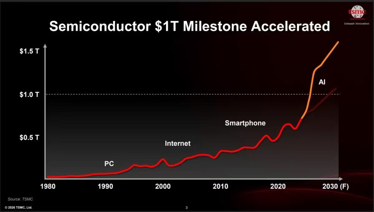
What once looked like a long march toward a one-trillion-dollar industry now appears to be happening much faster than expected. That matters because it suggests semiconductors are no longer just supporting the digital economy. They are becoming the core infrastructure of the AI economy, where compute, memory, packaging, and power all rise together.

A12, A13, and N2U are not just new node names — they show that advanced logic is no longer moving on a single track
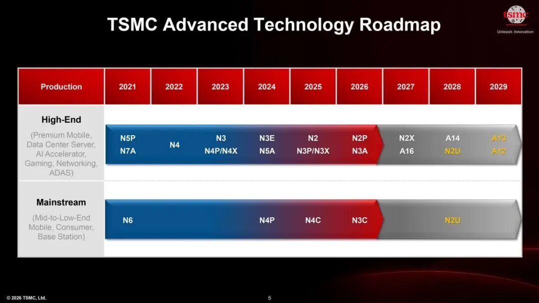
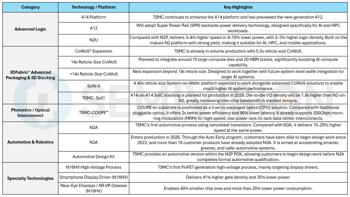
At its 2026 North America Technology Symposium in Santa Clara on April 22, TSMC unveiled its logic technology roadmap through 2029. The headline items included A13, A12, the unexpected N2 extension called N2U, and a continued decision not to use High-NA EUV for these nodes through 2029. TSMC also said A12 is scheduled for production in 2029, while N2U is targeted for production in 2028.

On the surface, this looked like a normal roadmap update: more node names, more performance claims, and one more round of “TSMC still does not need High-NA EUV yet.” But if that is all we see, we miss the deeper signal.
What TSMC really showed this week is that leading-edge logic is no longer evolving as one unified path. The roadmap now clearly reflects two different optimization philosophies: one for mobile and client platforms, where cost, power, IP reuse, and design continuity matter most; and another for AI and HPC, where power delivery, current density, wiring congestion, and peak performance have become central bottlenecks.
That distinction matters because the industry has already moved beyond the era when “the next node” meant roughly the same thing for everyone.
The old model of scaling is breaking apart
For many years, advanced-node competition was framed too simply: 7nm, then 5nm, then 3nm, then 2nm, and so on. The assumption was that whoever reached the next numerical milestone first controlled the technology narrative.

Source: TSMC
That framework is becoming less useful.
A smartphone SoC and an AI accelerator do not live in the same physical world anymore. A flagship mobile chip still cares deeply about leakage, battery life, area efficiency, analog/mixed-signal integration, and the ability to reuse proven IP blocks. By contrast, AI accelerators and HPC devices increasingly hit limits in power integrity, backside routing opportunity, local IR drop, package-level current delivery, thermal density, and system bandwidth economics. These are not marginal details. They are becoming first-order design constraints.
This is why TSMC’s roadmap feels structurally different. It is no longer just about transistor shrink. It is about segmenting the frontier.

On one side, TSMC continues to offer evolutionary platforms like N2P, N2U, A14, and A13, which improve performance-per-watt and density while minimizing redesign pain. On the other side, technologies like A16 and A12 are positioned more explicitly for workloads where traditional frontside scaling is no longer enough, and where features such as Super Power Rail backside power delivery become strategically important.
This is the real roadmap story: not just smaller nodes, but different classes of advanced nodes for different compute eras.

A13 is not radical. That is exactly why it matters.
Among the new announcements, A13 is especially revealing.


In modern chip development, the cost of moving to a new process is not just wafer price. The real burden includes IP migration, standard-cell requalification, analog porting, EDA flow retuning, signoff reruns, timing closure, physical verification, reliability qualification, software enablement, and schedule risk. For large SoC teams, that migration cost can be enormous.
For mobile and client chips, this is exactly the right answer. These products do not always need a heroic leap in raw compute. They often need a more disciplined combination of lower power, smaller die area, faster time to tape-out, and better amortization of prior R&D.
So A13 matters not because it is aggressive, but because it is economically intelligent scaling.

N2U shows that TSMC is turning each node into a platform, not a one-time product
If A13 is about extending A14 efficiently, N2U is about something even more important:platform monetization across time.

TSMC says N2U uses design-technology co-optimization to provide roughly 3–4% higher speed at the same power, or 8–10% lower power at the same speed, along with around 2–3% logic density improvement relative to N2P, while remaining compatible with N2P IP. TSMC also characterizes it as a balanced option for AI, HPC, and mobile applications that benefits from the maturity and yield strength of the broader 2nm platform.
This is highly significant.
As nodes become more expensive, not every product should move to a completely new transistor generation. Many chip companies want to extend an already-developed family: flagship first, then derivative products, then cost-optimized versions, then broader deployment. A platform like N2U allows that. It stretches the economic life of the N2 ecosystem without forcing a full migration event.
From a semiconductor strategy perspective, this is a very smart move. It means TSMC is not only selling wafer starts. It is managing lifecycle yield curves, ecosystem reuse, and customer ROI across multiple product waves.
That is where foundry competition increasingly lives.
The next phase of advanced manufacturing is not just who has the best transistor. It is who can create the best platform continuity around libraries, IP, PDK stability, yield maturity, risk reduction, and multi-year design leverage.
N2U is a textbook example of that philosophy.

The TSMC 2nm (N2) technology has received multiple NTOs.
The N2P technology provides a 5% performance uplift, while maintaining the same design rules as N2, and could account for the majority of N2 adoptions. N2P delivers an 18% speed improvement at the same power, a 36% power reduction at the same speed, 1.2 times logic density, and 1.15 times chip density over N3E.
N2X consists of two elements: the ultra-high performance standard cell and a high-speed device, that provide a combined (5% each) 10% speed boost. The high-speed device is selectively inserted into critical paths, maximizing performance with minimum power overhead.
2025年6月25日
A16 and A12 belong to a different world: AI and HPC can no longer rely on incrementalism
If A13 and N2U are about efficient continuity, A16 and A12 belong to the opposite side of the roadmap.
These nodes are for workloads that increasingly expose the limits of traditional frontside power delivery and conventional routing assumptions.
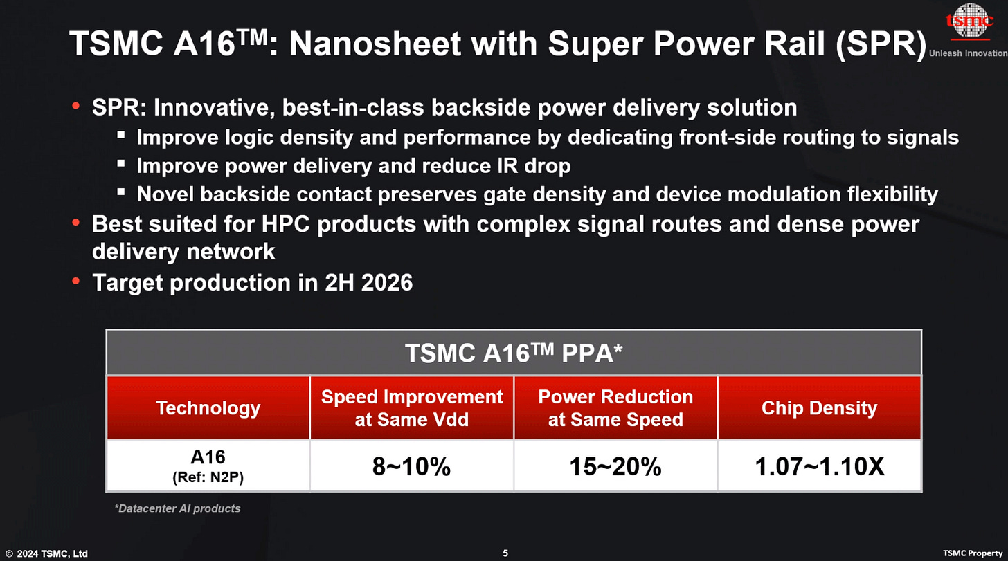
TSMC’s A16 incorporates Super Power Rail backside power delivery and is positioned as a high-performance technology for data-center-class applications. TSMC has said A16 will be ready in 2026, but volume production depends on customer demand and is now expected in 2027. A12, scheduled for 2029, is positioned as the next step beyond A16 and is expected to continue scaling both frontside and backside dimensions.

To understand why this matters, it helps to step back and look at the physics.
As AI chips scale up, the problem is no longer only transistor switching speed. The challenge increasingly shifts to delivering clean power and moving signals through an ever more congested stack. Frontside routing has to compete for area with signal wires, clock distribution, local interconnect, and power rails. At the same time, large AI dies draw enormous current, and current density creates IR-drop risk, electromigration concerns, and thermal concentration. When package-level current climbs and chiplet integration becomes denser, power delivery itself becomes a scaling bottleneck.
Backside power delivery is attractive because it separates power routing from signal routing. That can improve routing efficiency, reduce resistance in critical paths, and help recover performance or power headroom that would otherwise be lost to interconnect overhead. In practice, it is not magic. It adds process complexity and design implications. But for AI and HPC, it can be the difference between incremental gain and meaningful system-level benefit.
This is why A16 and A12 matter more than their labels suggest. They show that TSMC recognizes a new reality:
For AI infrastructure, the frontier is shifting from pure transistor shrink toward power-delivery architecture and holistic system enablement.

2025年7月3日

N2X still matters — because not every performance customer wants the same tradeoff
An interesting part of TSMC’s roadmap is that A16 does not eliminate the need for N2X.
N2X is essentially the high-frequency, performance-enhanced branch of the N2 family using more conventional frontside power delivery. That means TSMC still sees demand for customers who want to push clocks and performance while staying closer to a more established integration style, rather than adopting the full implications of backside power delivery immediately.
This is an important reminder that even within high-performance computing, demand is not uniform.
Some customers want absolute peak efficiency under future AI constraints. Others want faster deployment, lower transition risk, or better compatibility with existing flows. The winning foundry strategy is not to force everyone into one answer. It is to provide multiple on-ramps to the frontier.
TSMC is clearly building that menu.
2025年7月1日
The most interesting message may be what TSMC is not doing: High-NA EUV
Perhaps the most talked-about point from this year’s symposium is TSMC’s reaffirmation that it does not plan to use High-NA EUV for nodes like A13 and A12 through 2029. Kevin Zhang said TSMC’s technology team continues to find ways to scale without moving to High-NA yet, and emphasized that High-NA systems are extremely expensive. Reuters similarly reported that TSMC is aiming to maximize current EUV equipment rather than adopt ASML’s newer High-NA tools at this stage.
This is not a trivial decision.
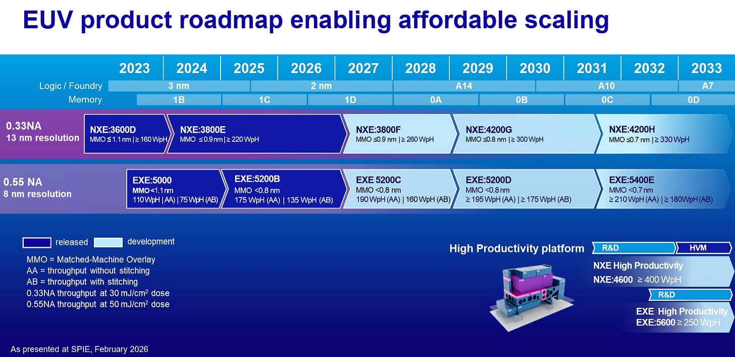
High-NA EUV is one of the most important lithography developments in the industry, but it comes with massive capital intensity, new ecosystem requirements, mask implications, process-integration complexity, and ROI questions. TSMC’s stance is effectively this:
If existing EUV can still deliver the needed scaling economically, then early adoption of High-NA is not automatically a virtue.
That is a very TSMC answer.
TSMC has long excelled not merely by advancing fast, but by choosingwhereto advance fast and where to extend the life of a mature manufacturing approach. In semiconductor manufacturing, this matters enormously. A node is not successful because it exists in slides. It is successful because it can be ramped at scale, with yield, with cost discipline, and with enough ecosystem support to attract large customer programs.
This is where TSMC’s strength shows. It is not just process leadership. It is manufacturing judgment.
And that is precisely why the High-NA question is so important. Intel has been much more public about adopting High-NA for future nodes, while TSMC is signaling that its competitive advantage may come from squeezing more value out of current EUV longer. These are two very different views of how to win the next decade of logic manufacturing.
3月20日
The hidden subtext: Moore’s Law is becoming a package-level story
Another important point mentioned in reporting around the symposium is that TSMC also discussed advanced packaging expansion, including the ability to stitch together far larger multi-die systems in coming years. Reuters noted that TSMC highlighted packaging capabilities involving up to 10 large compute dies with 20 memory stacks by 2028, illustrating how the performance frontier is increasingly moving from a single die to a multi-die package.
This matters because the roadmap should not be read in isolation from packaging.

In the AI era, the value of an advanced node depends not only on transistor density, but on how well it integrates with HBM, interposers, chiplet partitioning, thermal paths, reticle limits, yield strategy, and overall package power density. At leading edge, scaling is no longer “just lithography.” It is lithography plus backside power plus advanced packaging plus system interconnect plus thermal management.
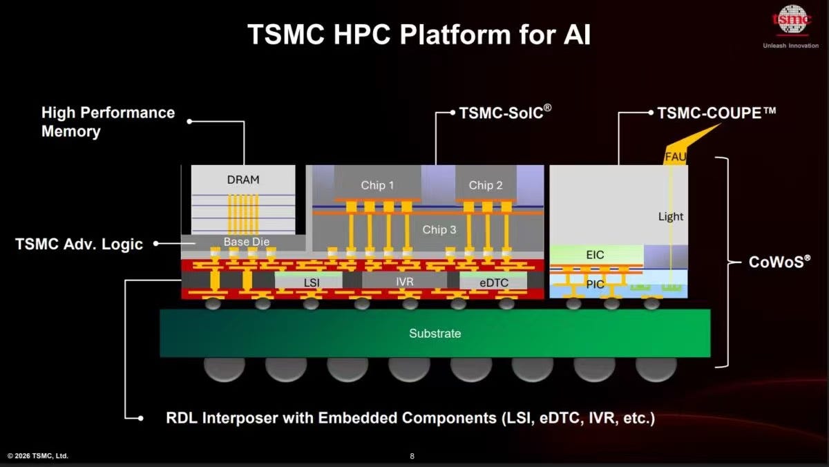
This is why TSMC’s node announcements must be understood alongside CoWoS, SoIC, and system integration. The market still likes to talk about nanometer labels. But real competitiveness increasingly comes from the combined stack.
In that sense, the most advanced semiconductor company is no longer simply the one with the smallest transistor. It is the one that can best orchestrate transistor technology, packaging, power delivery, and manufacturability into a system customers can actually ship at scale.

4月21日

TSMC’s silicon photonics development is becoming increasingly important because the bottleneck in AI infrastructure is no longer just compute density, but also how efficiently data moves between chips, packages, and racks. TSMC has been advancing its COUPE platform on PCB/Substrate and Interposer as a way to integrate photonic and electronic dies more tightly for high-performance computing applications.
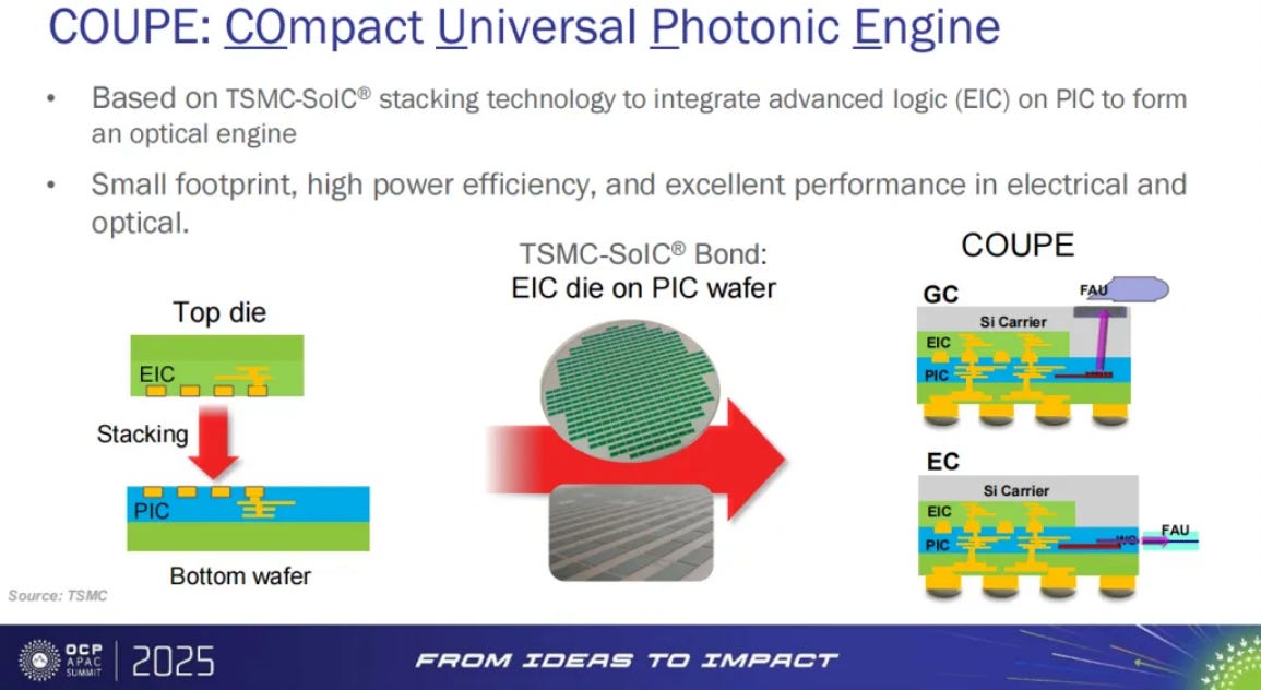
According to TSMC’s own research, COUPE is designed to support both grating-coupler and edge-coupler approaches while reducing insertion loss and improving structural robustness for co-packaged integration. TSMC has also said its first-generation COUPE, which combines an electrical chip and a photonics chip using SoIC bonding, has progressed well, showing that the company is not treating silicon photonics as a science project but as part of its broader advanced packaging roadmap.

2025年11月29日
What makes this especially strategic is that TSMC is linking silicon photonics to its packaging leadership. As AI systems scale beyond reticle limits and rely more on chiplets, HBM, and high-bandwidth interconnects, the value shifts from discrete optical modules toward tightly integrated optical I/O inside the package. COUPE is not just an optical device effort. It is part of TSMC’s larger attempt to extend its foundry advantage from transistor scaling into system-level integration
3月26日
What this roadmap really means
If we compress the whole story into one conclusion, it is this:
TSMC is no longer presenting advanced-node progression as a single linear race. It is presenting it as a segmented, platform-based manufacturing strategy designed for very different compute realities.
A13 and N2U represent one side of the future: lower migration friction, better IP reuse, stronger design ROI, and smoother platform continuity.
A16 and A12 represent the other side: AI- and HPC-driven scaling where power delivery, routing efficiency, and system-level performance matter more than simplistic node naming.
The absence of High-NA EUV through 2029 says something equally important: TSMC still believes the winning formula is not to adopt every new tool as early as possible, but to adopt technology at the point where it delivers measurable manufacturing and economic value.
That is the deeper meaning of this roadmap.

The semiconductor industry is entering a phase where the frontier is no longer defined only by who shrinks fastest. It is defined by who can answer four much harder questions at once:
Can you serve mobile and AI with different optimization targets?
Can you lower customer migration risk while still improving PPA?
Can you maximize capital efficiency while maintaining leadership?
Can you connect transistor scaling with power delivery and advanced packaging in a manufacturable way?
TSMC’s new roadmap suggests it believes the answer to all four is yes.
And if that is true, then the most important thing TSMC showed this week was not just A12 or A13.
It was that the company is trying to redefine leading-edge foundry competition itself.

4月17日
Thanks for reading SEMIVISION @_@! This post is public so feel free to share it.

2025年6月22日


PreviousNext