Intel’s New Strategy May Not Start With Leading-Edge Nodes, but With Advanced Packaging
Intel’s New Strategy May Not Start With Leading-Edge Nodes, but With Advanced Packaging
- Source: SemiVision
- Author: SEMIVISION
- Published: 2026-04-21T20:22:35+08:00
- URL: https://tspasemiconductor.substack.com/p/intels-new-strategy-may-not-start (1) Intel’s New Strategy May Not Start With Leading-Edge Nodes, but With Advanced Packaging


Intel’s New Strategy May Not Start With Leading-Edge Nodes, but With Advanced Packaging
Original Article By SemiVision Research [Reading time: 16 mins]

Apr 21, 2026
∙ Paid
Intel Is Quietly Changing Its Playbook: Not Leading With Advanced Nodes, but Securing the Advanced Packaging Entry Point?
On the surface, this news can easily be interpreted as just another routine foundry update: Intel is in talks for new orders, and the deal size appears meaningful.
But once the focus shifts from whether Intel is winning orders to what kind of orders it is winning, the story changes entirely.
What truly deserves market attention is not that Intel has secured a few more process customers, but that it is pushing advanced packaging to the forefront—and may even be positioning it as the primary entry point for Intel Foundry to gain traction. This is not a semantic nuance; it reflects a shift in strategic priority. Because in 2026, advanced process competition remains the most difficult battlefield to overturn, while advanced packaging represents a more pragmatic path—one that is far more aligned with the needs of the AI era.
Intel CFO Dave Zinsner made this point quite clearly at the Morgan Stanley Technology, Media & Telecom Conference. He noted that in earlier external communications, he had viewed the packaging business as being in the “hundreds of millions” range—essentially a supporting role compared to the tens-of-billions-dollar scale of future wafer foundry revenue. But that expectation has now been revised upward. He described packaging as a “very good business,” driven by demand from AI ASICs, with revenue potential “well north of $1 billion.” More importantly, he indicated that this segment could begin contributing even before meaningful wafer revenue materializes.
That statement is critical. It effectively acknowledges that Intel Foundry’s first real breakthrough may not come from process technology, but from packaging.
Behind this shift lies a broader industry reality—one that the market is gradually recognizing, but has not yet fully priced in. The competitive core of AI chips is moving away from how powerful a single chip can be, toward how multiple chips can be integrated into an efficient system. Advanced nodes still matter—no one disputes that. But as constraints around model scale, HBM capacity, die-to-die interconnect, power density, latency, and reticle limits all converge, the importance of system-level integration is rising rapidly.
This is precisely why advanced packaging is no longer just a back-end process. It is becoming a foundational layer of next-generation AI infrastructure.
Advanced Nodes Are Hard to Catch Up In. Advanced Packaging Looks More Like Intel’s Practical Breakthrough Point
Let’s put the conclusion first: if Intel wants to directly catch up with TSMC’s process leadership in the short term, the degree of difficulty remains very high. But if it shifts its approach and uses advanced packaging as the entry point into the hyperscaler AI ASIC supply chain, that path looks far more realistic.
The reason is not complicated.
Advanced process technology is a continuous trust competition. Customers do not judge a foundry only by the theoretical metrics of a single node. They care about whether it can deliver stable high-volume manufacturing, sustain ramp-up, maintain yield, ship on time, and stay on track across the next two or three generations of the roadmap. TSMC’s advantage here is not just about technical specifications. It is also about years of accumulated production records, customer relationships, and execution credibility. Reuters noted in March 2026 that Intel was still repositioning 18A for external customers, and that after Lip-Bu Tan took over, the company was reassessing the role of 18A as an external foundry offering. That alone suggests Intel has not yet reached the point where the market is fully confident in its advanced-node foundry business.
Packaging, however, is different.
Packaging is also difficult, and today it is no longer “low-tech” by any measure. But from the customer’s perspective, the decision logic is more about system integration capability, supply chain flexibility, and delivery capacity, rather than simply whether you are the most advanced logic-process supplier. When a customer designs its own AI ASIC and combines it with compute dies, I/O dies, or HBM from other sources, what it really needs is a partner that can reliably integrate those different chiplets, nodes, and functional blocks into a system-level packaging solution that can be manufactured at scale, cooled effectively, tested efficiently, and delivered on schedule. In that context, packaging becomes the main battleground, not a supporting role.
That is exactly the capability Intel is trying to sell.
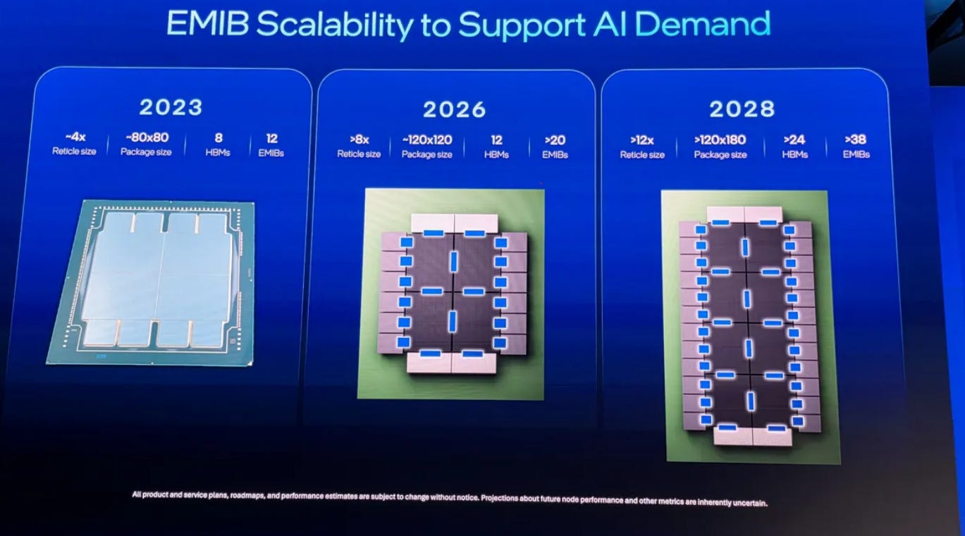
According to Intel’s official materials, Intel Foundry is now emphasizing an advanced packaging portfolio that includes Foveros 2.5D, Foveros Direct 3D, EMIB 3.5D, and EMIB-T for larger AI and HPC applications. Intel’s positioning is very clear: rather than forcing every function into a single monolithic die, these technologies allow customers to mix and match different process nodes and functional blocks through a chiplet architecture, break through reticle limits, and optimize power, bandwidth, and system flexibility at the same time. Intel has even stated directly that one of the advantages of EMIB and EMIB-T is their ability to support larger form factors and more flexible heterogeneous integration.
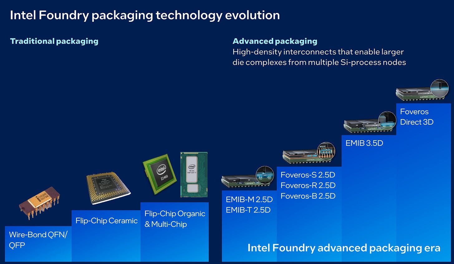
In other words, Intel is not saying, “We are now better than TSMC at making 2nm.” What it is saying is: if you already have an AI ASIC architecture, and you need larger packages, higher HBM bandwidth, and a more flexible chiplet configuration, I can help you build the system at the packaging level first.
That is a completely different competitive narrative.

2025年2月14日
Why Does the AI Era Need Packaging More Than Just Process Technology?
Because the bottleneck in today’s AI chips is increasingly no longer raw compute at a single point, but the constraints of the system as a whole.
For the past several decades, the competitive logic of the semiconductor industry was relatively straightforward: whoever had smaller transistors, higher density, faster frequency, and lower power consumption held the advantage. That was the classic front-end process story.
But the AI era is different.
Training and inference for large models require far more than a stronger compute die. They require larger memory pools, faster die-to-die interconnects, higher HBM bandwidth, lower energy consumption for data movement, and the ability to maintain signal integrity and thermal stability both within the package and across the broader system. Once a single die can no longer scale indefinitely, once HBM must sit ever closer to compute, and once the bottleneck of the overall system increasingly comes from data movement rather than arithmetic itself, packaging stops being a back-end support function and becomes a core part of system architecture.
That is why nearly every major AI chip player today—whether NVIDIA, AMD, Google, AWS, or an in-house ASIC team—ultimately has to confront the same reality: you may be able to design your own compute, but you cannot bypass packaging.
There is also another important difference between AI ASICs and traditional CPUs or GPUs: AI ASICs are becoming increasingly customized around specific workloads. That means customers are less likely to need a standardized, one-size-fits-all advanced process service, and more likely to need a partner that can quickly deliver heterogeneous integration and advanced packaging tailored to their system requirements. This is one of the key reasons hyperscalers are placing growing importance on packaging suppliers.
Why Are Customers Like Google and Amazon So Important?
Because they are not traditional fabless chip companies in the usual sense. They are the ultimate owners of AI infrastructure.
That is why these customers are not simply looking for a wafer vendor. They are looking for a system-level supply partner that can provide complete delivery capability.
And this is where a structural opportunity emerges that could be highly favorable for Intel.

Source: intel
If Intel today tries to persuade Google or Amazon to hand over their most critical leading-edge front-end manufacturing entirely to Intel, customers would likely remain highly cautious. But if what Intel offers is advanced packaging, chiplet integration, and HBM-related packaging capability—and if technologies such as EMIB, Foveros, and EMIB-T can help solve system-level bottlenecks for those customers—then the resistance to adoption becomes much lower. Because this is not a full-scale bet. It is a partial insertion. And in supply chain decision-making, the threshold for partial adoption is always lower than the threshold for a complete replacement.

Source: intel
That is why, even though current information related to Google and Amazon still comes mainly from media reports and no formal contract has yet been officially announced by Intel, the market should not treat it as just another ordinary rumor. From a commercial logic standpoint, this direction of cooperation is highly reasonable. And it also aligns closely with how Zinsner has described the opportunity in AI ASIC packaging.
This Is Not Just About Orders. It Is About Access.
Many investors tend to underestimate the strategic value of packaging orders because their instinct is to look at revenue scale: no matter how large packaging becomes, can it really compare with front-end wafer manufacturing?
That, however, is the wrong way to frame the question.
For Intel, this is not just a revenue issue. It is an access issue.
In the semiconductor supply chain—especially for products as complex as AI ASICs, where design cycles are long and qualification thresholds are high—once you become a qualified supplier in even one layer of the customer’s stack, you are no longer an outsider. You gain earlier visibility into the customer’s roadmap, a deeper understanding of its architectural requirements, and a better position in next-generation product discussions. From there, the opportunity can expand from packaging into testing, co-optimization, and even parts of process integration and design enablement. Once that relationship is established, the difficulty of winning larger business later drops meaningfully.
That is why the real importance of a multi-billion-dollar packaging deal may not be the revenue itself, but the position it gives Intel in the next-generation AI supply chain.
Is Intel still an outsider waiting at the door?
Or is it already a partner with one foot inside the hyperscaler in-house silicon ecosystem?
Those two positions carry completely different implications for valuation.
Why Does Intel Especially Need This Path Right Now?
Because it needs a path that allows the foundry story to revive in part, without first having to win across the board.
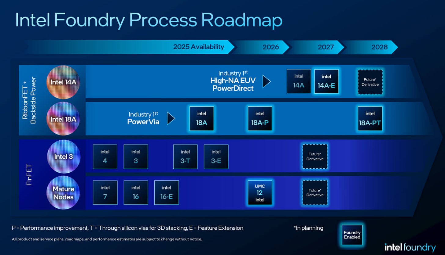
For years, market expectations around Intel Foundry were built largely on a highly ambitious script: use new nodes such as 18A and 14A to pull process technology back into the top tier, then win major external foundry customers. The problem with that path is that it stacks technological difficulty, capital intensity, time pressure, customer trust, and execution risk all on top of one another. The degree of difficulty is extremely high. If any one of those pieces slips, the entire market narrative slows down. Reuters’ March report this year also suggested that Intel was still adjusting how it positions 18A for external customers, which indicates that its foundry narrative is no longer as singularly centered on a dramatic comeback in advanced process technology as it once was.
Packaging offers a different recovery script:
not trying to catch TSMC head-on from day one, but first entering at the point where AI faces its greatest pain.
This path has three major advantages.
First, it aligns more closely with what the AI market actually needs today. What customers urgently need is not the supplier with the most compelling process roadmap story, but the one that can actually build, scale, and reliably deliver high-bandwidth, high-power, multi-chiplet systems.
Second, it fits Intel’s existing technology assets more naturally. Intel is not starting from zero in packaging. It already has Foveros, EMIB, and an expanding advanced packaging portfolio that includes EMIB-T. Compared with trying to re-establish credibility at the leading edge of process technology from a disadvantaged position, this is a much shorter path.
Third, it fits customer procurement logic better. Customers are far more willing to give you a trial order in a high-value portion of the stack than to immediately hand over their most critical leading-edge process business. A packaging order is exactly that kind of lower-resistance, but strategically high-value, entry point.

2025年6月3日
Can Advanced Packaging Pull Process Technology Forward in Return?
In theory, yes—and that is exactly the chain reaction Intel wants most.
Once packaging business reaches meaningful scale, Intel is no longer just selling a package. It begins selling a complete system solution. And in the chiplet era, design, process technology, packaging, and testing are becoming increasingly difficult to separate cleanly. Whoever can provide an integrated offering that combines process, packaging, and design services has a better chance of locking customers into its ecosystem.
That is also why Intel keeps emphasizing the idea of a “systems foundry” rather than a simple wafer foundry. What it wants to sell is not just wafers, but a full stack of capabilities spanning process technology, advanced packaging, and system-level co-optimization. In its official materials, Intel Foundry repeatedly highlights the value of combining process and advanced packaging to help AI and HPC customers build disaggregated, chiplet-based system architectures.
The real strategic upside here is this:
if a customer first adopts Intel because of packaging, and then in the next-generation design cycle discovers that certain chiplets, certain I/O dies, or certain specialized modules also make sense to place on Intel’s process platform, then the foundry relationship can naturally extend upward.
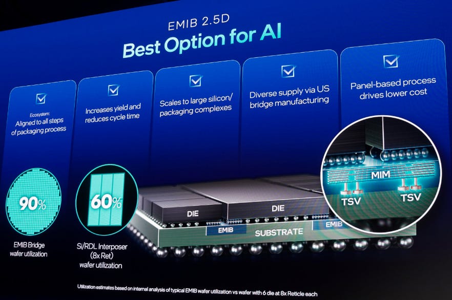
In other words, packaging is not a substitute for the foundry story. It may be the starting point that reopens it.
But This Path Is Not Without Risk
To stay objective, Intel’s packaging story—no matter how compelling—still cannot be treated as proof of a full turnaround.
There are at least four reasons.
First, much of what excites the market today is still in the discussion and expectation phase. Zinsner’s comments suggest that demand is strong and customer engagement is active, but that is not the same as a formal contract announcement. Google and Amazon have so far appeared mainly in external media reports, not on Intel’s official customer list. There is still distance between the two.
Second, advanced packaging is not a blue ocean. TSMC and Samsung are both pushing aggressively into this space, and many customers already have deep relationships with existing suppliers. Intel entering the field does not mean others will simply give up share.
Third, even if packaging is easier than leading-edge process technology as an entry point, it is still a manufacturing challenge with high demands on yield, materials integration, and testing. In large AI packages especially, involving HBM integration, thermal management, mechanical stress, and multi-layer supply chain coordination, a problem in any one link can slow mass production.
Fourth, packaging may help Intel secure a foothold, but that does not mean it automatically converts into a front-end process victory. That still requires a credible process roadmap, strong yields, customer trust, and sustained capital expenditure. If external commercialization progress on 18A and 14A does not improve in parallel, the market may ultimately view Intel only as a strong packaging supplier, rather than as a fully revived top-tier foundry.
4月8日
How Should the Market Reassess Intel?
I believe the key is not to frame Intel as a company that must “fully defeat TSMC,” but to rewrite the question as follows:
Can Intel first establish a presence in AI system integration that the market can no longer ignore?
If the answer is yes, then the market’s valuation logic does indeed need to change.
Much of the market’s pessimism toward Intel has been built on a linear assumption: Intel fell behind in process technology, therefore its foundry ambitions are broken; if foundry is broken, then it becomes marginalized in the AI supply chain; if it is marginalized in AI, then there is little room for valuation re-rating.
But if Intel has found another path—not by breaking through head-on in the transistor war, but by entering through packaging, integration, and the systems foundry model—then its recovery path is no longer about a full-scale catch-up. It becomes a partial breakthrough. And for a company of Intel’s size, a partial breakthrough is often far more realistic than an all-out comeback.
Put even more directly:
Even if Intel fails to win major leading-edge process orders, it could still enter the AI ASIC supply chain first through packaging.
If packaging reaches scale first, it can improve the commercial visibility of Intel Foundry and strengthen customer stickiness.
And if customers begin to accept Intel in the role of a systems foundry partner, the probability of extending that relationship into process technology later increases.
This logic does not mean Intel has already won.
But it does mean Intel may not need to win everything first in order to return to the center of the table.

Conclusion: What Intel Is Really Competing For Is Not Today’s Revenue, but Tomorrow’s Seat
So, back to the original question:
Is this merely a short-term order story, or has Intel found a new long-term breakthrough path?
My view is that in the short term, this is still mainly driven by order expectations and the pace of customer adoption. But in the medium to long term, it looks much more like the beginning of a structural breakthrough path.
The reason advanced packaging matters is not because it can immediately replace advanced process technology. It matters because in the AI era, it is precisely the layer that most directly connects chip design with system deployment. Whoever controls that entry point has a much better chance of becoming part of the next generation of AI infrastructure.
Seen through that lens, Intel’s current moves become much clearer:
it is not trying to prove first that it has fully caught up in the most advanced process technology;
it is trying to prove first that it still holds an indispensable position in the layer of the stack that AI needs most.
If Intel succeeds in this step, what it regains is not just tens of billions of dollars in revenue.
It regains a seat at the table where hyperscaler roadmaps and next-generation AI chip strategies are being decided.
I am more inclined to interpret this as follows:
Intel is using packaging as a springboard in an attempt to re-enter the core of the AI chip supply chain.
And that may be the part the market still has not fully priced in.
If an AI chip is not sent back to Taiwan for TSMC’s advanced packaging, Intel is arguably the strongest alternative in the United States. The reason is not simply geography. It is that Intel already has a real advanced packaging stack in place, including EMIB, Foveros, and newer EMIB-T offerings, and the company is positioning those technologies specifically around heterogeneous integration, HBM connectivity, larger package sizes, and system-level chiplet assembly. Intel says EMIB is already production-proven, supports logic-to-logic and logic-to-HBM integration, and offers a simplified supply chain and assembly path, while Foveros extends that capability into higher-density 3D stacking.
That matters because in the AI era, the bottleneck is often no longer just transistor scaling. It is how to combine compute dies, memory, I/O, and power delivery into one manufacturable, testable, and thermally manageable system. The video’s central point is that advanced packaging has become a strategic chokepoint, and if that work cannot be done through TSMC in Taiwan, Intel becomes the most credible U.S.-based fallback because it is one of the few players with an actual domestic advanced packaging footprint and a platform designed for large heterogeneous AI packages. Even so, the market should distinguish between Intel’s already deployed EMIB/Foveros capabilities and EMIB-T, which is still earlier in commercial adoption for external customers.
TSMC’s CoWoS capacity is expected to rise to roughly 115,000 to 140,000 wafers by the end of 2026, with a further increase to around 170,000 wafers in 2027. The main expansion sites are concentrated in Tainan and Chiayi, and the scale of this capacity build-out is significantly above the company’s historical pace. This suggests that TSMC is no longer making only incremental adjustments, but is entering a much more aggressive expansion cycle to support sustained AI-driven demand for advanced packaging.

2月23日


PreviousNext