Who Owns the Optical Layer? Lumentum’s Race to Control AI Interconnects
Who Owns the Optical Layer? Lumentum’s Race to Control AI Interconnects
- Source: SemiVision
- Author: SEMIVISION
- Published: 2026-04-12T13:08:08+08:00
- URL: https://tspasemiconductor.substack.com/p/who-owns-the-optical-layer-lumentums (1) Who Owns the Optical Layer? Lumentum’s Race to Control AI Interconnects


Who Owns the Optical Layer? Lumentum’s Race to Control AI Interconnects
Original Article By SemiVision Research [Reading time: 18 mins]

Apr 12, 2026
∙ Paid

AI Data Centers and the Shift to Optical Interconnects
Artificial intelligence, machine learning, and large-scale cloud computing are driving a fundamental transition in data centers—from traditional electrical interconnects to high-speed, low-power optical connectivity. As model parameters continue to scale, traffic within and between racks is surging, pushing copper interconnects close to their physical limits in both bandwidth density and thermal dissipation.
AI accelerators now require interconnect bandwidth at the hundreds of Tb/s level to efficiently share weights and activations. If electrical cables remain the primary medium, issues such as crosstalk, power consumption, and packaging constraints quickly become bottlenecks. As a result, leading chipmakers and cloud service providers are investing heavily in next-generation optical interconnect technologies. Among these, Co-Packaged Optics (CPO) is widely regarded as one of the most promising architectures.
CPO integrates optical transceivers directly adjacent to switching ASICs or compute chips, significantly shortening electrical paths and eliminating the interface losses and power overhead associated with traditional pluggable modules. In this paradigm shift, lasers serve as the fundamental “light source” of the system—their reliability and output power are critical.

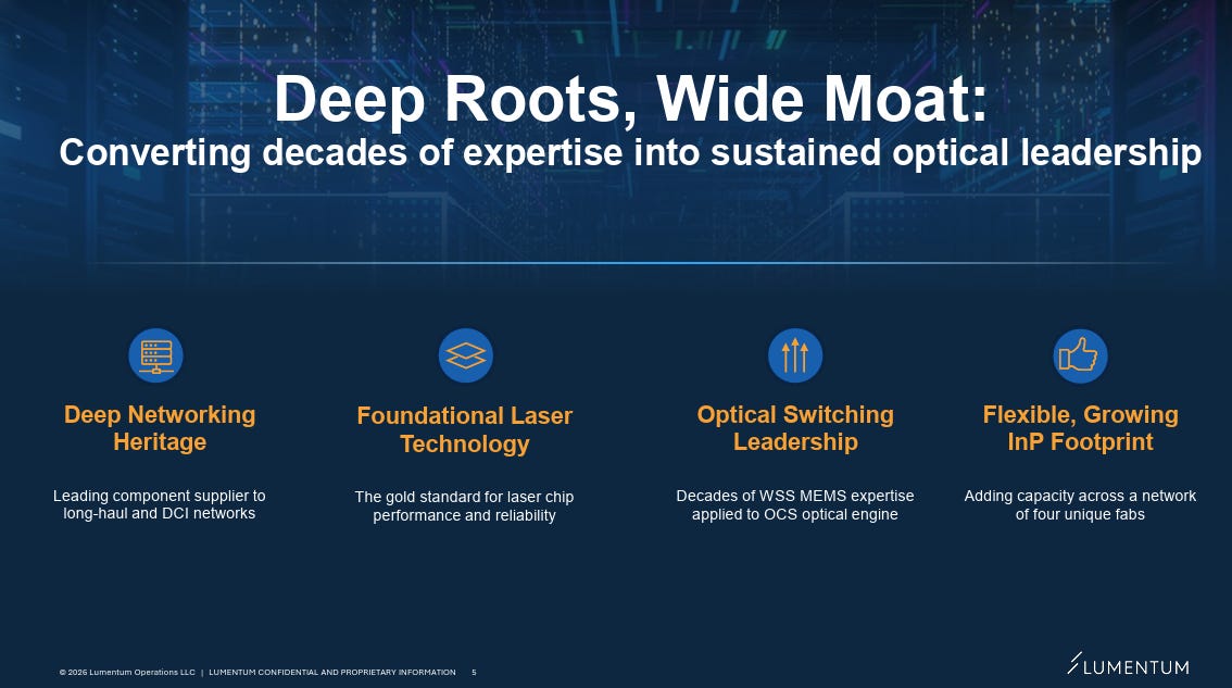
As one of the world’s leading optoelectronic manufacturers, Lumentum is leveraging its long-standing expertise in pump lasers and modulated laser technologies to drive innovation in CPO lasers, external light source modules, and capacity expansion. This article synthesizes multiple sources to provide a deep analysis of Lumentum’s technology roadmap, manufacturing strategy, and market outlook in the CPO era.
Overview of CPO Technology and Industry Drivers
Fundamental Principles of CPO
At its core, CPO tightly integrates continuous-wave (CW) lasers with silicon photonics chips placed in close proximity to switch ASICs or compute dies.
In traditional pluggable transceivers, electrical signals travel several centimeters or more between the ASIC and the optical module. This requires high-speed serializers/deserializers (SerDes) as intermediaries, leading to increased power consumption, higher latency, and concentrated thermal hotspots near the pluggable modules.
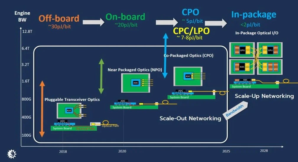
CPO fundamentally changes this architecture by co-packaging silicon photonics with the ASIC. Electrical trace lengths are reduced to the millimeter scale, enabling more efficient short-reach interfaces to replace long-reach SerDes. The result is significantly lower power consumption and substantially higher bandwidth density.
However, this architecture introduces new challenges—particularly in thermal management and reliability of optical components, especially lasers.
Two primary technical approaches are emerging:
External Laser Source (ELS) Architecture
High-power CW lasers are placed outside the ASIC package, typically at the front panel of the switch or rack. Light is delivered via optical fibers to the co-packaged optical engines.

Source: OIF
This approach keeps lasers away from high-temperature zones near the ASIC, reducing thermal stress while improving serviceability and replaceability.
Lumentum demonstrated its external laser solution—ELSFP modules—at ECOC 2025. These modules position the light source at the system front panel, offering modularity and maintainability while leveraging ultra-high-power (UHP) lasers.
Integrated CPO Architecture
As technology matures, lasers may be reintegrated into the package and more tightly coupled with silicon photonics.
This enables higher integration density but requires lasers with significantly improved thermal tolerance and lifetime reliability to operate within the harsh environment of advanced ASIC packaging.


3月14日
Industry Drivers
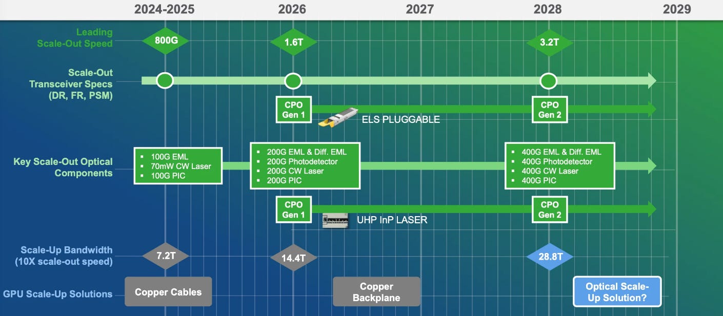
AI training clusters demand extremely high-speed data exchange across GPUs and TPUs. Switch port speeds have already evolved from 400 Gb/s to 800 Gb/s and 1.6 Tb/s, with 3.2 Tb/s on the horizon.
CPO enables higher port density and lower power consumption, making it a key enabler for scalable AI networking infrastructure.
Major industry players—including NVIDIA, Google, Microsoft, and Amazon—are actively investing in or developing CPO technologies. Notably, NVIDIA signed multi-billion-dollar investment agreements (reportedly around $2 billion each) with Lumentum and Coherent in 2026 to secure long-term laser supply.
Lumentum CEO Michael Hurlston highlighted at a Morgan Stanley conference that as the industry transitions from copper to optical interconnects, Indium Phosphide (InP) wafer capacity is becoming a critical bottleneck. NVIDIA’s investment is supporting the construction of Lumentum’s fifth wafer fab, ensuring long-term supply security.
NVIDIA Announces Strategic Partnership With Lumentum to Develop State-of-the-Art Optics Technology
Below we will share:
Lumentum High-Power Laser Technology
External Laser Source (ELS) Strategy: Bootstrapping CPO with ELS
Fab Footprint and Capacity Planning
Laser Roadmap: The Evolution of EML and CW
Market Outlook and Competitive Landscape
Conclusion: Lumentum’s Opportunities and Challenges in the CPO Era
Lumentum High-Power Laser Technology
1310 nm 400 mW Ultra-High-Power Lasers
In CPO architectures, optical engines typically require tens of watts of electro-optical power to drive dozens of channels. As a result, lasers must deliver output power exceeding 22 dBm (approximately 160–316 mW) at the 1310 nm wavelength, while maintaining high power conversion efficiency and narrow linewidth characteristics.
Lumentum, in collaboration with partners such as Meta, has developed continuous-wave (CW) lasers capable of exceeding 400 mW output while sustaining over 10% electro-optical efficiency. Research publications indicate that by adopting an Indium Phosphide (InP) dual-cavity distributed feedback (DFB) structure, these lasers can achieve up to 880 mW output at 25°C and still maintain 580 mW at 50°C, all while preserving single-mode operation. This provides substantial optical power headroom for CPO applications.
Further reports from Converge Digest highlight that Lumentum’s 1310 nm 400 mW laser leverages decades of experience in pump laser technology to address longstanding challenges in CPO—particularly laser fragility and limited lifetime. By adapting pump laser designs originally developed for submarine optical systems, Lumentum has achieved reliability levels comparable to those required for undersea deployments.
This was also confirmed by CEO Michael Hurlston at a Morgan Stanley conference, where he noted:
“Submarine pump lasers cannot be replaced frequently, so their reliability must be extremely high. We are bringing that same technology into CPO lasers.”
UHP Laser Product Characteristics
According to Lumentum’s official specifications, its Ultra-High-Power (UHP) lasers operate at 1311 nm and deliver:
Up to 350 mW output at 50°C
Approximately 235 mW output at 70°C
Power conversion efficiency exceeding 20%
Linewidth below 500 kHz, meeting stringent requirements for low relative intensity noise (RIN) in CPO systems
These lasers are built on an InP platform, enabling both high reliability and narrow spectral linewidth. They have already been integrated into ELSFP modules and pluggable solutions, supporting large-scale deployment in AI data centers.
Within ELSFP modules, lasers are precisely temperature-controlled באמצעות dual thermo-electric coolers (TEC), enabling stable operation and single-wavelength output up to 24 dBm (~250 mW). The architecture also allows multiple silicon photonics engines to share a single laser source, reducing the number of lasers required per port and thereby lowering both system cost and power consumption.

Source: Lumentum
Pump Laser Reliability and Telcordia Standards
Lumentum’s ability to deliver highly reliable CPO lasers is rooted in its deep expertise in pump laser technology. Its 980 nm and 14xx nm pump lasers are widely used in erbium-doped fiber amplifiers (EDFAs) and Raman amplifiers, and are designed to meet the extreme reliability requirements of long-haul and submarine optical communication systems.
According to official documentation, Lumentum’s pump lasers comply with the stringent Telcordia GR-468-CORE standard, ensuring long-term stability and reliability. These submarine-grade quality control methodologies have been extended to its CPO laser portfolio, enabling reliability levels that can pass 24-hour burn-in testing and meet the demands of hyperscale AI data center environments.
External Laser Source (ELS) Strategy: Bootstrapping CPO with ELS
ELS Architecture and Its Advantages
In the early evolution of CPO, Lumentum has advocated the use of an External Laser Source (ELS) architecture. ELS moves high-power lasers from the ASIC package and places them in pluggable, serviceable modules (ELSFP), which then deliver light to silicon photonics engines via optical fibers.

Source: Lumentum
Demonstrations at ECOC 2025 showed that positioning the laser source on the system front panel—rather than near the chip package—significantly improves thermal management and reliability while increasing overall system density. Because the lasers are physically separated from heat sources and can be independently replaced, system maintainability and serviceability are greatly enhanced.
Lumentum’s ELSFP module provides a complete external laser solution. It integrates ultra-high-power (UHP) CW lasers, thermal control, power delivery, and monitoring interfaces, and connects to CPO optical engines through standard fiber interfaces. According to official descriptions, the ELSFP module enables multiple silicon photonics engines to share a single laser source through a centralized, serviceable architecture, while maintaining output performance at 1311 nm and up to 24 dBm.
Coverage fromSemiconductor Today,further emphasizes that by decoupling the laser from the optical engine, ELSFP modules improve thermal performance and lifetime reliability, enabling higher system density and lower thermal load for high-bandwidth data centers.

Turnkey Solutions and Customer Demand
Many cloud service providers and chip companies lack deep expertise in optical system design, while deploying CPO requires complex laser driving and thermal management.
At the 2026 Morgan Stanley conference, CEO Michael Hurlston noted that most customers are not optical experts and therefore require more complete turnkey solutions. By offering fully integrated ELS modules, Lumentum enables customers to deploy CPO without needing to deeply understand laser driver design, significantly lowering the technical barrier to adoption.
This approach not only benefits new entrants in the AI infrastructure space, but also opens up new revenue streams for Lumentum.
During its February 2026 earnings call, Lumentum indicated that expanding into external light source modules can increase revenue per laser chip by2–2.5×. The company emphasized that the external light source business expands its addressable market and diversifies its customer base, as many partners adopting next-generation scaling architectures require more complete turnkey solutions.
This strategy aligns with the industry’s transition path: starting with ELS and gradually moving toward deeper co-packaged integration.

In-House Laser Platform and ECOC Demonstrations
Lumentum’s ELSFP modules are built on fully in-house InP laser technology combined with mature module packaging processes. According to company disclosures, these modules achieve long-term stable operation through dual-TEC temperature control, narrow linewidth stabilization, and optical power monitoring.
At ECOC 2025, Lumentum demonstrated ELSFP modules based on UHP 1310 nm lasers, targeting 800G and 1.6T switches and AI processors, enabling high-density optical interconnects.
These demonstrations lay the groundwork for future fully integrated CPO architectures. As laser technology matures to the point where it can be re-integrated into the package, the same UHP laser chips can be reused in more tightly integrated designs.
At the same time, Lumentum is developing single-chip 400 mW-class lasers, ensuring that future fully co-packaged solutions can deliver both high optical power and compatibility with in-package integration constraints.
Fab Footprint and Capacity Planning
Four Existing Fabs and a New Fifth Facility
As of early 2026, Lumentum operates four Indium Phosphide (InP) wafer fabrication facilities located in Japan (two sites), the UK, and San Jose in the United States. Disclosures from the Morgan Stanley conference indicate that Lumentum is allocating capacity across these fabs based on product type:
Japan (Sagamihara and Takao):
Focused on the production of EML (Electro-Absorption Modulated Lasers) and CW lasers for traditional pluggable transceivers and scale-out optical interconnects.
UK (Caswell):
Originally planned to produce EMLs, CW lasers, and some photodetectors. With the surge in CPO demand, the facility is being repurposed as a CPO-dedicated fab, while retaining limited photodetector production capacity.
U.S. (San Jose):
Fully cleared and reconfigured to focus exclusively on high-power lasers for CPO. The site has already begun volume production and shipment of high-power lasers, with capacity expected to be rapidly absorbed by CPO demand in the coming months.
In addition, Lumentum is leveraging NVIDIA’s $2 billion investment to build a fifth InP wafer fab. According to Reuters, CEO Michael Hurlston confirmed that the new facility will be constructed in the United States to expand capacity and meet NVIDIA’s multi-year procurement commitments. NVIDIA also stated that the investment is intended to establish new U.S.-based manufacturing capacity to support the scaling of AI factories through optical interconnect components.
Capacity Expansion and Long-Term Agreements
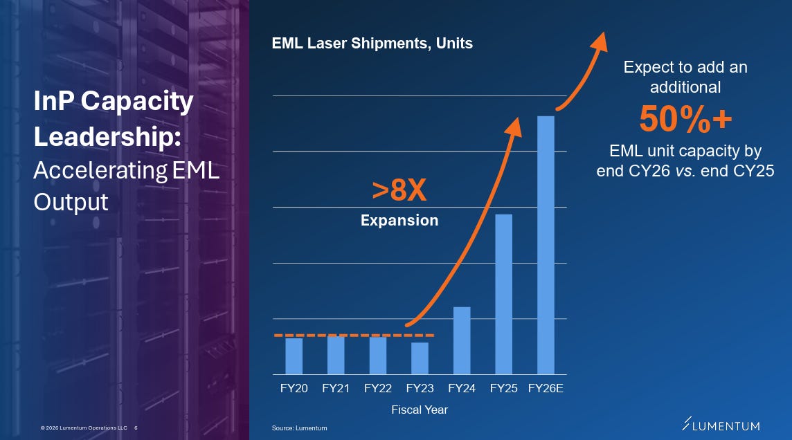
In its fiscal 2026 Q2 earnings report, Lumentum disclosed that its InP wafer capacity is expanding rapidly, yet still remains supply-constrained.
The company has already completed approximately 40% of its planned capacity expansion in Japan, accelerating output through process optimization and yield improvements, while also utilizing underused capacity in both the UK and Japan.
However, even with these expansions, all incremental EML capacity has already been fully booked under long-term agreements through the end of 2027. These agreements secure committed volumes from customers and allow Lumentum to optimize pricing amid tight supply-demand conditions.

At the Morgan Stanley conference, Michael Hurlston emphasized that despite ongoing capacity expansion—both by Lumentum and its competitors—current demand levels imply that capacity may be effectively sold out through 2027 and potentially into 2028:
“Based on current demand, we are essentially sold out through 2027—and possibly into 2028. We simply cannot produce enough lasers.”
This dynamic positions Lumentum’s InP laser capacity as a scarce strategic resource, and highlights the importance of NVIDIA’s early capacity reservation strategy.

3月4日
San Jose Expansion and U.S. Manufacturing
In August 2025, Lumentum announced a major investment to expand its Indium Phosphide (InP) wafer fabrication facility located on Rose Orchard Way in San Jose. The site is dedicated to the production of ultra-high-power (UHP) lasers, targeting next-generation Co-Packaged Optics (CPO) platforms.
According to the company’s press release, the expansion is designed to strengthen the domestic AI supply chain by leveraging the inherent advantages of InP lasers—namely low power consumption, high efficiency, and long-term reliability. The project is also expected to create hundreds of high-skilled jobs in advanced photonics manufacturing.
Additional coverage from Optics.org noted that the expansion will increase capacity not only for UHP lasers, but also for EMLs (Electro-Absorption Modulated Lasers), CW lasers, and coherent optical components. This positions Lumentum to meet rapidly growing demand from both CPO deployments and cloud-scale data center infrastructure.
As collaboration with NVIDIA deepens, the San Jose facility has been further transformed in early 2026 into a CPO-dedicated production line, with high-power laser shipments already underway. This transition marks a critical shift from general photonics manufacturing toward AI infrastructure-specific components.
From a strategic perspective, the San Jose fab is becoming a key anchor for Lumentum’s U.S.-based manufacturing footprint. It strengthens the company’s positioning in securing semiconductor incentives, enhances supply chain resilience, and builds trust with hyperscale customers seeking geographically diversified and politically aligned production capacity.

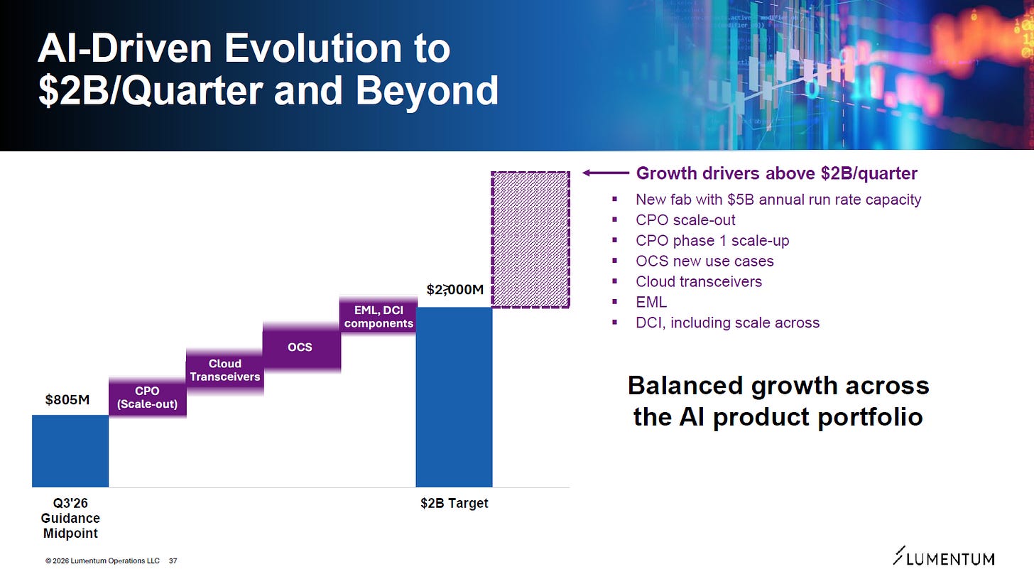
Lumentum’s broader UHP laser manufacturing strategy: a newly acquired UHP laser fab—purchased from Qorvo in Greensboro, North Carolina—is expected to support up to $5 billion in annual revenue capacity. As a fully operational compound semiconductor facility, it enables faster time-to-production, with the deal officially closing on March 17, 2026. Lumentum plans to ramp UHP laser output by early 2028. Taken together, the San Jose expansion and this new U.S. fab acquisition point to a clear strategic direction: scaling InP-based laser capacity as a critical foundation for next-generation AI and CPO infrastructure.
Caswell Transition in the UK and Japan Operations
The Caswell facility in the UK was originally used for EML and CW laser production. At the Morgan Stanley conference, CEO Alan Lowe Hurlston indicated that the site is being converted into a dedicated CPO facility, while continuing to produce a limited volume of photodetectors. This shift signals that demand for CPO is now growing faster than the EML market. The construction of a fifth wafer fab is expected to further ease supply–demand constraints.
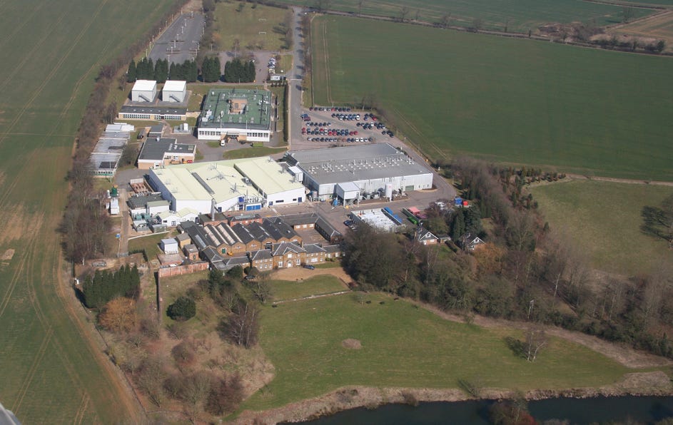
Caswell manufactures indium phosphide optical modulator chips, which can be found in many of Lumentum’s products.
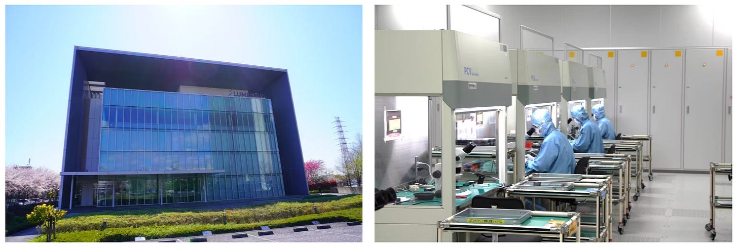
Meanwhile, the Sagamihara and Takao plants in Japan continue to manufacture 100G/200G EMLs and standard CW lasers. Financial disclosures show that 200G EML chips currently account for about 5% of shipment volume but contribute roughly 10% of revenue due to higher ASPs. By the end of 2026, their share is expected to rise to 25%, further improving gross margins. At the same time, the company plans to complete 40% of its EML capacity expansion ahead of schedule.
Laser Roadmap: The Evolution of EML and CW
Laser Choices in the 1.6 Tb/s Era
As the market transitions toward 1.6 Tb/s, the industry is debating whether to continue using EMLs (electro-absorption modulated lasers) or shift toward continuous-wave (CW) lasers paired with silicon photonic modulators. At the Morgan Stanley conference, analysts suggested that “early 1.6T demand will primarily rely on EML, but may shift toward CW lasers over time.” In response, Hurlston explained:
The scaling of CPO will replace part of the pluggable transceiver market, so we do not need to make a large-scale transition between EML and CW.
He expects that in the mid to late stages of the 1.6T cycle, as CPO and silicon photonics adoption increase, the share of CW lasers will rise. However, existing 100G/200G EML capacity is expected to be fully utilized for several years.
Internally, all transceivers produced by the company use CW lasers combined with silicon photonics, so a portion of CW capacity will be reserved for internal use.
This indicates that in the short term, EML will remain the dominant solution for 1.6T modules. However, as silicon photonics matures, CW lasers will gain advantages in higher-density port architectures. At the same time, CPO will further accelerate the adoption of CW lasers. Industry sources such asSemiconductor Todayalso note that the long-term roadmap beyond 1.6T is expected to shift from EML toward CW lasers integrated with silicon photonics, with optical interconnects gradually replacing copper links as CPO and optical engines become more widespread.
EML Supply Remains Tight
Despite the long-term shift toward CW lasers, near-term demand for EML remains extremely strong. In its 2026 financial report, Lumentum disclosed that demand for 100G and 200G EMLs exceeds supply by approximately 30%, with newly added capacity already locked in through long-term agreements extending to the end of 2027.
At the Morgan Stanley conference, Hurlston emphasized that all available EML capacity will be fully absorbed by the market—and still fall short of demand—so there are no plans to reallocate capacity toward CW lasers at this stage.
Market Outlook and Competitive Landscape
Explosive Demand from AI and Cloud Computing
AI model sizes are growing exponentially, with leading models now reaching tens of billions—or even trillions—of parameters. Communication bandwidth has become a critical bottleneck for training efficiency.
Take the NVIDIA GB200 NVL72 system as an example: a single rack integrates 72 Grace Hopper compute modules, requiring hundreds of 800G/1.6T interfaces for full interconnect both within and across racks. Deployments of such systems are expected to scale rapidly over the next few years, driving a surge in demand for lasers and optical engines.
Lumentum has stated that it has already secured long-term purchase agreements from multiple major customers and is expanding its ultra-high-power (UHP) laser capacity accordingly.

3月17日
Co-Development of CPO and OCS (Optical Circuit Switching)
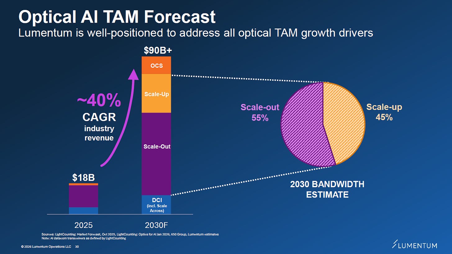
Lumentum categorizes its future growth drivers into three segments: cloud switching modules, optical circuit switching (OCS), and CPO.
OCS leverages technologies such as wavelength selective switches (WSS) to enable dynamically reconfigurable optical backplanes within data centers, reducing the number of electrical switching layers. In fiscal 2026, Lumentum has already achieved over $4 million in OCS revenue ahead of schedule, with significant growth expected in the second half of 2027.

CPO and OCS are complementary and can be deployed together in AI clusters: CPO addresses interconnects between ASICs and optical engines, while OCS optimizes connectivity across racks and data center fabrics.
3月26日
Competitors and Ecosystem Partners
Key competitors include Coherent, Broadcom, and Ayar Labs.
Coherent has also signed long-term agreements with NVIDIA and benefits from 6-inch InP wafer technology, providing advantages in cost and scale. Broadcom focuses on silicon photonics-based optical engines, while Ayar Labs specializes in optical I/O using microring modulators.
Lumentum, however, maintains a leading market share in UHP lasers and EMLs, and has established close partnerships with major hyperscalers such as NVIDIA and Meta.
Its strategy is to expand InP capacity, lock in customers through long-term agreements, and move into external laser source (ELS) modules to increase customer stickiness. While its customer base is concentrated among a few hyperscale clients—bringing both stable demand and concentration risk—the current supply shortage of UHP lasers may also attract competitive capacity expansion and potential pricing pressure in the future.

3月16日
Geopolitical Risks and Supply Chain Strategy
Given that InP wafer substrates rely on a limited number of suppliers and global trade dynamics could impact material availability, Lumentum has secured a seven-year long-term agreement with non-China suppliers to ensure substrate supply for its Japan operations.
This agreement extends into the mid-2030s, helping mitigate potential export control risks. The company is also evaluating acquisitions to fill capacity or technology gaps, although its primary focus remains on internal execution and capacity expansion.

3月10日
Conclusion: Lumentum’s Opportunities and Challenges in the CPO Era
Lumentum is undergoing a transformation from a traditional telecom component supplier into a core enabler of optical interconnects for the AI era.
By launching 1310 nm 400 mW ultra-high-power lasers, developing external laser source (ELS) architectures, strategically planning wafer fab capacity, and securing significant investment from NVIDIA, the company has built a strong competitive moat in the CPO space. At the Morgan Stanley conference, Lumentum outlined a clear division of its three fabs—dedicated respectively to EML/CW, CPO, and photodetectors—fully aligning capacity toward CPO. At the same time, it is leveraging its long-standing expertise in pump laser reliability and Telcordia standards to address lifetime challenges in CPO laser systems.
However, challenges remain. While EML will continue to dominate in the early phase of 1.6T, the long-term trajectory is shifting toward CW lasers and silicon photonics. Lumentum must carefully balance its investments between EML and CW technologies. Whether its capacity expansion can keep pace with explosive customer demand, and how it manages pricing power amid customer concentration, will be critical in the coming years.
As OCS and CPO scale, optical interconnects are expected to increasingly replace copper links within data centers. Lumentum is well positioned to capitalize on this transition through its laser and ELS solutions.
In summary, Lumentum has already established a leading position in CPO technology, products, and capacity planning. By continuously improving laser power, enhancing reliability, expanding wafer capacity, and delivering turnkey solutions, the company is building a solid foundation for the next wave of AI-driven data center optical interconnect demand. As sixth-generation data centers move toward 3.2T and beyond, Lumentum’s roadmap will continue to push deeper integration between optics and silicon—shaping the next era of optical communications.
Thanks for reading SEMIVISION @_@! This post is public so feel free to share it.


PreviousNext
TopLatestDiscussions








See all