The Next Battlefield for AI Chips: From Training to Inference
The Next Battlefield for AI Chips: From Training to Inference
- Source: SemiVision
- Author: SEMIVISION
- Published: 2026-04-07T10:39:58+08:00
- URL: https://tspasemiconductor.substack.com/p/the-next-battlefield-for-ai-chips (1) The Next Battlefield for AI Chips: From Training to Inference


The Next Battlefield for AI Chips: From Training to Inference
Original Article By SemiVision Research [Reading time: 35 mins]

Apr 07, 2026
∙ Paid
The Next Battlefield for AI Chips: From Training to Inference
The next major battleground in AI chips is shifting—from training processors to inference chips. This transition is not incremental; it is a structural shift driven by the explosive growth of generative AI applications.

Recently, waves of viral use cases—such as Ghibli-style image generation—have triggered a surge in inference demand. OpenAI CEO Sam Altman noted that he had never seen usage grow this fast, openly stating that OpenAI’s GPU resources are now fully saturated. As a result, large models like GPT-4.5 must be released in stages, initially limited to Pro users due to the sheer scale of required compute.
This pressure is not unique to OpenAI. Meta and other AI leaders are facing similar GPU bottlenecks. While GPUs are extremely powerful, they were not originally designed for continuous, large-scale inference workloads. The result is high power consumption, limited efficiency, and growing systemic strain across the AI infrastructure stack.

2025年4月18日
This is why the market is rapidly shifting toward inference-optimized architectures—including NPUs (Neural Processing Units) and custom ASICs. These chips deliver significantly better performance-per-watt compared to general-purpose GPUs.
OpenAI is already moving in this direction. The company has begun developing its own AI chips, targeting mass production around 2026, in an effort to reduce dependence on NVIDIA. At the infrastructure level, OpenAI and Microsoft are also advancing the “Stargate” super data center initiative, reportedly involving up to $500 billion in investment.
This signals a clear reality:
AI inference is becoming a strategic pillar on par with data centers, cloud infrastructure, and semiconductors.
From Training-Centric to Inference-Driven AI
We are now seeing a fundamental shift in AI architecture priorities.
Historically, AI development focused on training—building larger models, improving accuracy, and scaling compute. But as applications like ChatGPT, AI copilots, and intelligent agents become mainstream, the industry is realizing a critical truth:
The real value of AI does not come from training. It comes from inference.
Every interaction, every generated token, every query answered—these are all inference events. AI is transitioning from a one-time training investment into a continuous consumption model.
In this new paradigm:
Training = CapEx
Inference = recurring revenue
AI is no longer just a technology. It is becoming a metered compute engine.
Why Inference Chips Matter More Now

Inference chips are fundamentally different from training chips.
While both are AI accelerators, their design priorities diverge significantly:
Training chips: maximize throughput, support massive parallelism
Inference chips: optimize latency, efficiency, and cost per query
Inference workloads require:
Low latency (real-time interaction)
High efficiency (cost control)
Scalability (mass deployment across users and devices)
This is why specialized architectures are emerging across the industry:
Google → TPU
Amazon → Inferentia
Meta → in-house ASICs
Startups → Groq, Tenstorrent, Cerebras
Each is targeting one goal: optimize inference at scale.

3月30日
NVIDIA: From Training Leader to Inference Empire
At the center of this shift, NVIDIA is not standing still. It is expanding.
The company is evolving from a training-era leader into a full-stack inference powerhouse.
Its latest architecture, Blackwell, is designed with a clear objective:
reduce the cost per token while increasing throughput.
This is critical. Because when inference becomes cheaper, usage increases. And when usage increases, the entire AI economy expands.
This creates a powerful feedback loop:
Lower cost → More usage → Higher demand → Larger infrastructure scale
This is the engine behind AI’s exponential growth.
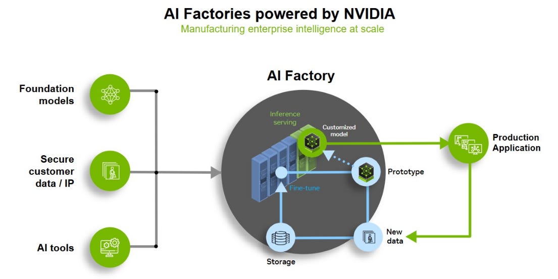
System-Level Scaling: The Rise of AI Factories
NVIDIA’s strategy goes beyond chips.
With systems like NVL72, NVIDIA is building large-scale, tightly integrated GPU clusters that behave like a single massive compute unit. This “scale-up” architecture is designed to handle:
Longer context windows
More complex reasoning
Multi-step AI workflows
As AI evolves from simple Q&A into agent-based systems, small distributed setups are no longer sufficient. The future demands:
Higher integration
Lower latency
Greater bandwidth
In other words, AI infrastructure is becoming centralized, dense, and system-driven.

3月17日
The Real Moat: Software, Not Hardware
What truly differentiates NVIDIA is not just hardware—it is its software ecosystem.
From CUDA to TensorRT-LLM and inference optimization stacks, NVIDIA is transforming from a chip vendor into a full AI infrastructure provider.
Companies are no longer just buying GPUs. They are adopting an entire AI factory platform.
This creates:
High switching costs
Deep ecosystem lock-in
Industry-wide standardization
Cloud providers—including Microsoft, Oracle, and CoreWeave—are aligning with this architecture, further reinforcing NVIDIA’s dominance.
At this point, NVIDIA is not just a supplier.
It is becoming the center of the AI ecosystem.
The Rise of AI Agents Will Accelerate Inference Demand
Another key trend is the rise of agentic AI.
Future AI systems will not just respond to prompts—they will:
Plan tasks
Execute workflows
Interact with tools
Replace parts of human labor
These systems require:
Lower latency
Higher memory bandwidth
More persistent compute
Which means one thing:
Inference demand will not just grow—it will accelerate.
AI Has Become a Consumption Economy
The AI industry is undergoing a fundamental transformation.
Compute is no longer just a technical metric—it is directly tied to revenue generation. GPUs are no longer just hardware—they are token-generating machines. Within this framework, NVIDIA is redefining the AI business model by controlling the stack—from chips to systems to software.
And the industry is following.
In one sentence:
NVIDIA is transitioning from the leader of the training era to the rule-maker of the inference era.
And the future of AI will be defined by three variables:
Cost. Efficiency. Scale.
This is not just a shift in chip design. It is a turning point for the entire digital economy.

Design Characteristics of Training Chips
The training phase involves processing massive datasets and requires both forward and backward propagation to update model weights, resulting in extremely high computational demands. Therefore, training chips must support high-density matrix operations and gradient calculations, and are typically deployed in distributed systems using multiple GPUs or TPUs.
High-Performance Compute Cores
Training chips are equipped with a large number of compute cores to support large-scale matrix operations and deep neural network training.
Large Memory Capacity and High Bandwidth
To handle massive training datasets, training chips require large-capacity memory (such as HBM) and high-bandwidth data transfer channels to ensure fast data access.
Scalability
Training chip architectures must support multi-chip scalability, enabling coordinated operation across multiple devices for large-scale model training.
Design Characteristics of Inference Chips
The inference phase only requires forward propagation to generate predictions based on pre-trained weights, without updating parameters. While computational demand is relatively lower, inference chips must meet strict requirements for low latency, high throughput, and low power consumption—especially for edge and real-time applications.
Low Power Consumption
Inference chips are designed to operate in power-constrained environments, such as mobile devices and edge systems, with a strong emphasis on energy efficiency.
Real-Time Responsiveness
Inference chips must deliver fast processing speeds to support real-time applications, such as speech recognition and autonomous driving.
Specialized Hardware Acceleration
Inference chips often include dedicated hardware accelerators for specific operations (e.g., matrix multiplication, convolution) to improve efficiency.
As AI technology continues to evolve rapidly, both training and inference chips are advancing in design to meet the demands of different application scenarios. Understanding these differences is essential for selecting the right hardware platform and achieving optimal performance and efficiency in AI deployments.

2025年7月4日
A Turning Point in the AI Chip Race: From Training to Inference
Over the past few years, the focus of AI chips has been overwhelmingly centered on the training phase. As large language models and multimodal models rapidly scaled, the industry pursued larger parameter counts, higher compute density, and stronger training performance—driven by the logic of the Scaling Law.
However, as AI transitions from the lab into real-world applications, market priorities are shifting. The demand for practicality and efficiency is rising quickly. Increasingly, attention is moving beyond training itself toward what happens after training is complete—the post-training stage.The Rise of the Post-Training Era
In this stage, two major trends are emerging.
First, techniques such as fine-tuning, LoRA, and adapters are being widely adopted to refine models for specific tasks and datasets. These methods improve accuracy, stability, and domain-specific performance during inference.
Second, inference itself is becoming more sophisticated. Instead of simply running a model, systems now:
Dynamically adjust prompt structures
Decompose complex problems into multiple steps
Introduce multi-model collaboration
These approaches significantly increase reliance on inference compute. What was once a bottleneck primarily during training is now extending into the inference stage—at much larger scale.
The Shift in the Competitive Landscape
As a result, the center of gravity in the AI chip market is undergoing a fundamental shift.
The competition is moving away from a training-centric GPU market toward a more diverse ecosystem of inference-focused hardware, including:
NPUs (Neural Processing Units)
ASICs (Application-Specific Integrated Circuits)
FPGAs and other customized architectures
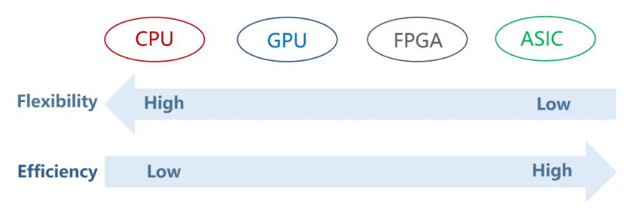
Whether in large-scale data centers delivering AI services or edge devices requiring real-time responses and low power consumption, inference chips are rapidly becoming critical.
This transition is not just about reallocating compute resources. It represents a deeper transformation across:
AI system architecture
Commercial deployment strategies
Supply chain structures
Training vs. Inference: From Computational Differences to Strategic Shifts
To understand this structural change, it is essential to examine the fundamental differences between training and inference workloads. These differences shape not only chip design, but also market positioning and competitive strategy.
Training: Massive Compute, Long Cycles
Take today’s dominant Transformer architecture as an example. Since the release of “Attention Is All You Need” by Google in 2017, Transformers have become the foundation of large language models such as GPT, Claude, and Gemini.

During training, models process massive paired datasets (e.g., translation corpora) and continuously update weights through forward and backward propagation. This process involves:
Extremely large-scale matrix operations
Gradient calculations
Parameter updates
Training typically requires weeks or even months of distributed computation across GPUs or TPUs.
Inference: Simpler Compute, Harder Constraints
Once training is complete, the system enters the inference phase.
Here, computation becomes structurally simpler:
Only forward propagation is required
Inputs (often tokenized) are processed using pre-trained weights
No gradient updates or backpropagation are needed
As a result, inference typically requires an order of magnitude less compute than training.
However, this does not mean inference is easy.
The real challenge lies in:
Low latency→ users expect instant responses
High throughput→ providers must handle massive query volumes
Cost efficiency→ reducing cost per query is critical
These requirements are fundamentally different from training, which prioritizes maximum performance regardless of latency.
Why Inference Chips Are Architecturally Different
Because of these constraints, inference chip design focuses on different priorities:
Energy efficiency (performance per watt)
Data movement optimization
Memory hierarchy and bandwidth utilization
Hardware-software co-optimization
This explains why many companies—both startups and hyperscalers—are choosing not to compete directly with NVIDIA in training GPUs. Instead, they are building inference-optimized architectures.
New Wave of Competitors
Across the industry, we are seeing a surge of innovation in inference hardware:
Amazon → Inferentia
Google → Edge TPU
Startups → Groq, Tenstorrent, Cerebras, SambaNova
These players are differentiating across:
Dataflow architecture
Chip area allocation
Power efficiency
Memory access patterns
Compute core design
Their goal is clear: outperform GPUs in inference efficiency and cost structure.

2025年9月12日
The Real Challenge to NVIDIA
For NVIDIA, this shift represents a new kind of challenge.
While GPUs continue to dominate the training market, the inference space is becoming increasingly competitive. Inference chips are no longer a secondary option—they are becoming the primary compute engine across:
AI cloud services
Edge devices
Embedded systems
Real-time applications
Under the dual forces of hardware evolution and application expansion, the AI chip landscape is rapidly transitioning:
From “training-first” to “inference-first.”

2025年5月6日
From Training-Centric to Inference-Driven AI
The AI industry is entering a new phase.
Training will remain essential—but it is no longer the center of value creation. The real economic engine of AI lies in inference: every query, every response, every generated token.
This shift is redefining:
Chip architecture
Infrastructure design
Business models
And ultimately, it is reshaping the entire competitive landscape of the semiconductor industry.
In one sentence:
The AI chip race is no longer about who trains the biggest model—but who can run it most efficiently at scale.
Competition in the Inference Chip Market: NVIDIA’s Challenge and the Rise of New Players
As inference becomes the new focal point of AI computing, a growing number of companies and startups are moving away from reliance on general-purpose GPUs. Instead, they are developing chip architectures specifically optimized for AI workloads—particularly Transformer-based models.
This shift is creating an unprecedented challenge for NVIDIA, which has long dominated the AI training chip market.
Custom Architectures for a New Workload
From a technical perspective, inference workloads are inherently simpler than training. They do not require gradient computation or weight updates, which opens the door for more specialized and efficient hardware designs.
As a result, many companies are building custom AI accelerators:
Meta→ MTIA (Meta Training and Inference Accelerator)
Amazon→ Inferentia and Trainium
Google→ TPU (training) and Edge TPU (inference at the edge)
Startups→ Groq, Cerebras, Tenstorrent, SambaNova
These architectures are specifically optimized for Transformer workloads, delivering advantages such as:
High throughput
Low latency
Superior energy efficiency
Below we will share:
From General-Purpose to Workload-Specific: The Real Battle in Inference Chips
Understanding Inference Chips Is Key to Understanding AI’s Future
Application Perspective: Demand Diversification from Cloud to Edge Devices
Major Technology Companies Introduction (NVIDIA, Intel, Groq, Cerebras Systems, Hailo, Graphcore, Huawei, Cambricon, Alibaba Group)
From General-Purpose to Workload-Specific: The Real Battle in Inference Chips
One of the most important shifts in today’s AI hardware landscape is the move away from general-purpose GPU design toward highly specialized, workload-specific architectures. Instead of attempting to support a wide range of computing tasks, a new generation of chips is being purpose-built for AI inference—focusing on the core operations that dominate modern models, particularly matrix multiplication, attention mechanisms, and optimized dataflow. This targeted design philosophy allows for far more efficient allocation of silicon area, memory bandwidth, and compute resources. In specific workloads, these chips can deliver meaningful advantages over traditional GPUs, including higher speed, better power efficiency, and lower cost per inference. In other words, they are not trying to be universally flexible—they are trying to be precisely optimal.
However, despite these architectural advantages, emerging players face a fundamental constraint: the software ecosystem gap. NVIDIA has spent more than a decade building one of the most complete AI computing platforms in the industry. Its stack—ranging from CUDA, cuDNN, TensorRT, NCCL to Triton—integrates seamlessly with dominant frameworks such as PyTorch and TensorFlow. Beyond tools, it also includes extensive model libraries, highly optimized kernels, and mature deployment platforms. This ecosystem dramatically lowers the barrier for developers to build, tune, and deploy AI applications at scale. For many organizations, the decision is not just about chip performance, but about developer productivity, time-to-market, and system reliability—areas where NVIDIA maintains a significant advantage.
NVIDIA’s Platform Advantage
Beyond software, NVIDIA’s strength is further amplified by scale. With deep financial resources and a dominant market position, the company can continuously invest across the entire stack—from hardware innovation to software optimization and system-level integration. The launch of H100, for example, was not just a chip release, but a full-stack rollout, paired with Hopper-optimized tools, dedicated frameworks for generative AI workloads, and high-bandwidth interconnect technologies such as NVLink and NVSwitch. This level of integration transforms GPUs from standalone components into part of a cohesive “AI factory” infrastructure. Combined with CUDA’s entrenched position, it creates a powerful lock-in effect that is extremely difficult for new entrants to replicate in the short term.
As a result, while the inference chip market is now filled with innovation and new competitors, NVIDIA continues to maintain strong dominance through its platform-level advantage and economies of scale. The competitive dynamics going forward will hinge on two critical questions: whether emerging players can overcome developer lock-in and build sufficiently mature software ecosystems and supply chain capabilities, and whether NVIDIA can continue evolving its inference offerings to defend against increasingly specialized architectures. This makes it clear that the competition is no longer confined to hardware specifications alone.
It is now a full-stack battle—spanning ecosystems, developers, and platform strategies.
Understanding Inference Chips Is Key to Understanding AI’s Future
Ultimately, understanding inference chips is key to understanding the future of AI. They are no longer a secondary component of the system; they are becoming the core engine that drives real-world applications, economic value, and scalable deployment. As the industry shifts from training-centric to inference-driven computing, the competitive landscape of AI chips is being fundamentally redefined—not by who can build the most powerful hardware, but by who can deliver the most efficient, integrated, and scalable system.
As AI technology moves into a phase of real-world deployment, it is becoming increasingly clear that the center of gravity in the chip market is shifting—from training to inference. This transition is not only reshaping technical design choices, but also redefining business strategies across the industry. More importantly, it provides a clearer lens through which we can understand the next phase of the AI chip market.
At the chip design level, the rise of inference is driving a shift from general-purpose architectures toward task-optimized designs. We are seeing innovation emerge beyond traditional GPU paradigms. For example, Cerebras adopts a wafer-scale engine approach, addressing data movement bottlenecks at the physical level, while Groq emphasizes software-defined compute, using static scheduling to extract maximum efficiency through tight hardware-software co-design. These approaches highlight the growing diversity of AI chip architectures and signal a departure from the historically GPU-dominated design mindset led by NVIDIA.
At the same time, NVIDIA’s platform advantage remains formidable. Years of investment in its software stack—including CUDA, cuDNN, and TensorRT—combined with a mature ecosystem spanning models, drivers, and development frameworks, continue to create a high barrier for competitors. While startups and hyperscalers are introducing compelling innovations in specific architectures and use cases, NVIDIA still maintains a clear lead in overall development maturity, deployment readiness, and ecosystem integration.

2月26日
Chip Design Perspective: From General-Purpose Architectures to Task-Optimized Design
On the application side, the evolution of inference chips is increasingly driven by diversification of use cases. Beyond cloud-centric applications such as large language models and generative AI, demand is rapidly expanding toward edge and endpoint environments. These include AI perception and decision-making systems in autonomous vehicles, real-time response modules in robotics, as well as inference workloads in wearable devices and smart home systems.
Application Perspective: Demand Diversification from Cloud to Edge Devices
Such scenarios impose strict constraints on power consumption, form factor, and latency—very different from large-scale GPU deployments in data centers. As a result, a broader range of inference chip designs is emerging, including Tesla’s Dojo, custom ASICs, autonomous driving chips such as NVIDIA Orin and Mobileye EyeQ, and highly integrated NPUs. This signals that the future of inference chips will not follow a single technological trajectory, but rather evolve along multiple parallel paths, each tailored to specific application requirements.
In summary, only by deeply understanding both the design logic and application drivers behind inference chips can we grasp the next wave of transformation in the AI chip market. From data centers to edge devices, from software platforms to hardware architectures, inference has become the new core battleground for innovation. And ultimately, this competition will determine how fast—and how far—AI can scale into widespread, real-world adoption.
Here is your content rewritten into a structured English article with clear sections:
Evaluating HBM Demand for AI Chips: A Comparative Analysis of Training and Inference Workloads
As generative AI models continue to scale rapidly, HBM (High Bandwidth Memory) has become a critical technology in pushing the performance limits of AI chips. Whether in training or inference, HBM plays a central role in data throughput, latency control, and energy efficiency—directly impacting overall system performance. However, due to fundamental differences in computational characteristics and memory usage patterns, training and inference workloads require distinct approaches when evaluating HBM capacity and bandwidth.
- Training Phase: Memory-Intensive and Bandwidth-Driven
AI model training involves repeated forward and backward propagation, along with continuous weight updates. This process places extremely high demands on both memory capacity and bandwidth.
Take the example of a large language model such as LLaMA 2 70B. With tens of billions of parameters, even at FP16 precision, the required memory footprint per GPU can approach or exceed 140 GB, far beyond the 80 GB HBM capacity of NVIDIA H100. As a result, training such large models typically requires model parallelism or sharding across multiple GPUs.
In addition, training workloads are highly I/O intensive, often requiring 1 to 3 TB/s of memory bandwidth. The pressure becomes even more pronounced when using large batch sizes and long context lengths, making bandwidth a primary bottleneck. This is why advanced training accelerators—such as NVIDIA H100, AMD MI300X, and Intel Gaudi 3—commonly adopt HBM3 or higher, emphasizing bandwidth density as a key design metric.
- Inference Phase: Latency-Sensitive and Efficiency-Oriented
Inference differs fundamentally from training. Instead of updating parameters, the system performs forward propagation on pre-trained models to generate outputs in real time. Memory usage in this stage is more focused on frequent lookups and reads, rather than continuous updates.
For example, while a model like GPT-3 175B still requires loading large model weights during inference, techniques such as:
Model partitioning
Quantization (INT8, INT4)
Sparse activation (e.g., Mixture-of-Experts, MoE)
can significantly reduce memory pressure on a single device.
Inference bandwidth requirements typically fall within the range of 300 to 700 GB/s, depending on model architecture and context length. However, as sequence lengths increase—such as in multi-turn conversations or long-form content generation—bandwidth constraints can become more pronounced.
This is why modern inference accelerators, such as NVIDIA L40S and Google TPUv5e, still rely on high-performance HBM to ensure stable latency and throughput.
- HBM Evolution and Selection Guidelines
HBM technology continues to evolve rapidly:
HBM3→ up to ~819 GB/s per stack
HBM3e→ up to ~1.2 TB/s per stack
HBM4 (future)→ expected to exceed ~1.6 TB/s per stack, with total bandwidth surpassing 13 TB/s through multi-stack configurations
For future models exceeding trillions of parameters, HBM4 is likely to become a standard requirement.

2月5日
When evaluating or designing AI chips, HBM selection can be guided by the following principles:
Training Workloads
Prioritize memory capacity (ability to hold model weights)
Ensure sufficient aggregate bandwidth for large-batch, high-throughput training
Recommended baseline: HBM3 or higher
Inference Workloads
Focus on latency and energy efficiency
Maintain sufficient bandwidth headroom for real-time or high-concurrency applications
Combine with quantization and optimization techniques
Hybrid Deployment (Training + Inference)
Balance capacity, bandwidth, and thermal design
Prefer architectures supporting HBM3e or modular scaling
Optimize for flexibility across dynamic workloads (e.g., cloud platforms)
The role of HBM in AI systems is no longer optional—it is foundational. However, its optimal configuration depends heavily on workload characteristics. Training demands maximum capacity and bandwidth, while inference prioritizes efficiency, latency, and scalability.
Understanding these differences is essential for making informed decisions in AI chip design and deployment. As models continue to grow and applications become more real-time and distributed, HBM will remain at the center of the AI infrastructure stack, shaping both performance limits and system architecture in the years ahead.

Major Technology Companies
NVIDIA:As the global leader in the GPU market, NVIDIA continues to drive the advancement of AI inference technologies. The company offers a range of high-performance inference solutions, including the H100, L4, and Grace Hopper Superchip, complemented by software platforms such as Triton Inference Server to support AI inference workloads across cloud, data center, and edge environments.
The H100, based on NVIDIA’s Hopper architecture, is a flagship GPU designed for both training and inference. It features fourth-generation Tensor Cores with support for FP8 precision, enabling significant performance gains for large language models (LLMs). Compared to its predecessor, the A100, the H100 delivers up to 4× faster training and 30× higher inference performance for models such as GPT-3. It also offers 900 GB/s of GPU interconnect bandwidth, making it well-suited for high-performance computing (HPC) and large-scale AI deployments.
The L4 is a power-efficient inference GPU designed for both edge and data center applications. It supports a wide range of AI workloads, including computer vision, speech processing, and recommendation systems. Compared to traditional CPU-based inference, the L4 can deliver up to 6× higher performance while maintaining strong energy efficiency. This makes it particularly suitable for real-time processing in edge devices and scalable cloud services.

2025年4月26日
The Grace Hopper Superchip combines NVIDIA’s Grace CPU with the Hopper GPU, connected through a proprietary chip-to-chip (C2C) interconnect that provides up to 7× the bandwidth of PCIe. It integrates up to 480 GB of LPDDR5X memory, enabling a unified memory architecture that is highly effective for memory-intensive AI inference and HPC workloads.

2月28日
On the software side, NVIDIA offers the Triton Inference Server, an open-source platform designed to streamline AI deployment. Triton supports multiple deep learning frameworks, including TensorFlow, PyTorch, and ONNX, and provides advanced features such as dynamic batching, model parallel execution, and pipeline orchestration. It can be deployed across cloud, data centers, and edge environments, delivering consistent and high-performance inference while simplifying model deployment and lifecycle management.

3月11日
Intel:Through its in-house Gaudi family (originating from Habana Labs) and Meteor Lake processors, Intel is focused on delivering integrated hardware–software AI solutions, with particular emphasis on emerging applications such as robotics and autonomous agents.
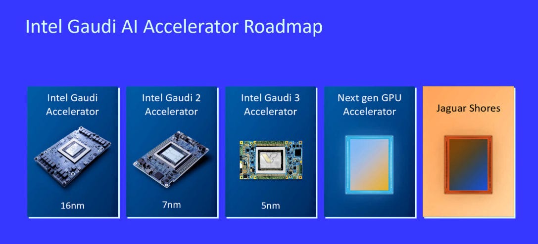
Intel’s strategy in AI acceleration can be broadly divided into two main directions: first, the Gaudi series of AI accelerators targeting cloud and data center markets; second, the Meteor Lake processors aimed at client and edge applications. Together, these product lines reflect Intel’s end-to-end approach—from high-performance training platforms to low-power inference devices—especially for emerging use cases such as robotics, smart manufacturing, and autonomous agents, enabled by tightly integrated hardware and software solutions.
The Gaudi family originates from Intel’s 2019 acquisition of the Israeli AI chip startup Habana Labs. Designed for both AI training and inference workloads, the Gaudi lineup—from the original Gaudi to the latest Gaudi 3—has steadily advanced in compute performance and interconnect capabilities. Gaudi 3 is built on a 5nm process and features 128GB of HBM2e memory, while supporting standard Ethernet-based networking. Compared to GPU architectures that rely on proprietary interconnects, this approach offers greater flexibility and improved cost efficiency. For large language model training (e.g., GPT-4–class models), Gaudi 3 delivers more than a 2× performance improvement in FP8 precision over its predecessor, making it particularly well-suited for high-density, distributed AI training workloads.

On the client and edge side, Intel has introduced a dedicated Neural Processing Unit (NPU) for the first time in its Meteor Lake processors, signaling its strong push into on-device inference. Built using Foveros 3D packaging technology, Meteor Lake integrates CPU, GPU, NPU, and SoC components into a single module. Its NPU incorporates dual AI engines capable of supporting applications such as speech recognition, image generation, and on-device generative AI, all while operating at extremely low power. This enables real-time processing with minimal impact on battery life and overall system performance, making Meteor Lake particularly well-suited for laptops, embedded robotics, and intelligent edge devices.
On the software side, Intel provides a comprehensive development stack—including oneAPI, OpenVINO, and the Habana SynapseAI SDK—to help developers optimize deployment and accelerate inference across different hardware platforms. The Gaudi series offers native support for PyTorch and integrates with mainstream frameworks such as Hugging Face, while Meteor Lake’s NPU is being aligned with toolchains like Windows AI Studio to accelerate the adoption of on-device AI.
Overall, Intel is steadily transforming from a traditional processor vendor into an integrated AI platform provider. Its product portfolio—spanning data center training to edge inference—positions the company to enhance efficiency across the entire AI model lifecycle and to drive the broader adoption of generative AI and autonomous agent technologies across diverse industry applications.

2025年6月3日
Groq’sLanguage Processing Unit (LPU) is a purpose-built accelerator designed specifically for large language model (LLM) inference. Its core objective is to deliver extremely high throughput and ultra-low latency, making it particularly well-suited for real-time natural language applications such as voice assistants, live translation, and generative AI responses. At the heart of the LPU is a deterministic design philosophy, ensuring that each token is processed at a consistent and predictable rate, thereby minimizing latency variability.

The LPU adopts a single-core streaming architecture, which avoids the scheduling overhead and resource contention commonly found in multi-core compute designs. This architecture enables fully serialized execution with highly predictable data flow, making it especially effective for token-by-token LLM inference. In contrast to traditional GPU architectures that rely heavily on High Bandwidth Memory (HBM), Groq’s LPU leverages large amounts of low-latency SRAM to improve memory access efficiency while reducing power consumption.
The LPU architecture is derived from Groq’s earlier Tensor Streaming Processor (TSP), which emphasizes static instruction scheduling and optimized dataflow. Compute units and memory are tightly interleaved to maximize data locality and utilization efficiency. This design enables exceptionally high token throughput in LLM inference workloads. Groq has demonstrated performance of up to 253 tokens per second on Llama2-70B, 473 tokens per second on Mixtral, and over 800 tokens per second on Gemma, with latency consistently maintained around 0.3 seconds.
On the software side, Groq provides a comprehensive toolchain and development environment, including the Groq Compiler, which automatically translates high-level models (such as those built in PyTorch) into optimized LPU instruction sets. The GroqCloud platform offers cloud-based inference services with precise, token-based billing. Developers can rapidly deploy inference workloads via APIs, leveraging Groq’s growing model support ecosystem, which includes major open-source models such as Llama2, Gemma, and Mixtral.
Overall, Groq’s LPU represents a simultaneous innovation across both hardware and software layers, achieving strong performance across key AI deployment metrics—throughput, latency, and energy efficiency. Rather than competing directly with NVIDIA GPUs in training, Groq’s strategy focuses on maximizing performance in the inference phase of LLMs, positioning the LPU as a compelling new option for both data center and edge inference applications.
Cerebras Systems :Introduced the Wafer Scale Engine (WSE), a chip with hundreds of thousands of cores designed to support large-scale AI model training and inference, alongside cloud-based services.

The Wafer Scale Engine (WSE) developed by Cerebras Systems is currently the largest AI-dedicated chip in the world. Its latest generation, WSE-3, is manufactured using TSMC’s 5nm process and integrates up to 4 trillion transistors and 900,000 AI cores. With a die size of 46,225 mm², it far exceeds the scale achievable by conventional chip designs. Beyond its record-breaking physical size, the WSE architecture significantly enhances AI training and inference efficiency through massive core density and expanded on-chip data pathways.
WSE-3 delivers up to 125 petaflops of AI compute performance and features orders of magnitude more on-chip memory and internal bandwidth than traditional GPUs. Its high-density SRAM is tightly integrated with compute units, minimizing data movement between memory and processing elements—one of the primary sources of latency and energy consumption in AI workloads. According to official claims, WSE-3 achieves over 50× higher compute density and performance compared to the NVIDIA H100 GPU.
Cerebras deploys WSE-3 within its CS-3 system, an integrated solution purpose-built for large language model (LLM) training and inference. The CS-3 delivers twice the performance of its predecessor and is capable of completing full training runs of massive models such as Llama2-70B in less than a day. In addition, Cerebras has built a supercomputing network called Condor Galaxy, which connects multiple CS systems to deliver exaflops-scale compute, making it one of the few platforms globally capable of handling ultra-large-scale AI models.
To expand AI accessibility, Cerebras also offers cloud-based inference services via APIs, using token-based billing. These services provide extremely low latency and high throughput for LLM inference. For example, when running Llama3.1-70B, the system can achieve inference speeds of up to 450 tokens per second—significantly outperforming traditional GPU-based architectures. This capability has been adopted by startups such as Perplexity AI and Mistral AI for applications in search, generation, and conversational AI.
Beyond commercial applications, the WSE architecture is also being applied in advanced scientific research and healthcare. Cerebras Systems has collaborated with the U.S. Department of Energy on high-performance simulation workloads, and with Mayo Clinic to develop genomics-driven predictive models. This breakthrough chip design offers a faster and more energy-efficient alternative for large-scale AI training, reshaping the computational foundation across domains ranging from data center infrastructure to precision medicine.
Amazon Web Services (AWS) and AI chip company Cerebras Systems have announced a collaboration to launch a high-speed inference solution for generative AI and large language model (LLM) workloads. The solution will be deployed on the Amazon Bedrock platform within AWS data centers, combining AWS’s in-house AI chip AWS Trainium with the Cerebras CS-3 system to significantly accelerate AI inference performance.

According to AWS, this collaboration adopts an “Inference Disaggregation” architecture, which splits the AI inference pipeline into two distinct stages: prefill and decode. The prefill stage is responsible for processing user input prompts and is highly parallelizable, requiring substantial compute resources. In contrast, the decode stage generates output tokens sequentially, typically accounting for the majority of inference time and demanding high memory bandwidth.
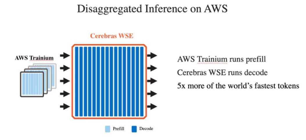
In this architecture, AWS Trainium handles the prefill stage, while Cerebras CS-3 is dedicated to decode operations. The two systems are connected via the high-speed Elastic Fabric Adapter (EFA), enabling each processor to optimize for the workloads it handles best. AWS stated that this division of labor could improve overall inference performance by an order of magnitude compared to existing solutions.

2025年6月2日
Hailo:Known for its Hailo-8 and Hailo-15 AI accelerators, Hailo focuses on edge AI inference for applications such as autonomous driving and smart cameras.
Hailo is an artificial intelligence chip company headquartered in Tel Aviv, Israel. Founded in 2017 by Orr Danon, Avi Baum, Hadar Zeitlin, and Rami Feig, the company specializes in designing high-performance AI processors optimized for edge devices. Its mission is to bring data center–class deep learning capabilities to edge environments such as smart cameras, autonomous vehicles, and industrial robots.

Hailo’s core product lineup includes the Hailo-8 and Hailo-15 chips:
Hailo-8:
This AI accelerator delivers up to 26 TOPS (trillion operations per second) while consuming only around 2.5 watts, achieving exceptional power efficiency. It features a unique dataflow architecture that enables efficient execution of deep learning models under tight power constraints. Hailo-8 is well-suited for applications such as autonomous driving, smart cities, and industrial automation.
Hailo-15:
Designed as an AI vision processor (VPU) for smart cameras, Hailo-15 provides up to 20 TOPS of compute performance. It integrates an image signal processor (ISP) and supports high dynamic range (HDR), enabling high-quality imaging even in low-light environments. The Hailo-15 family includes three variants—Hailo-15H, Hailo-15M, and Hailo-15L—targeting different performance tiers. These chips are ideal for use cases such as smart city surveillance, traffic management, and retail analytics.
Graphcoredevelops the Intelligence Processing Unit (IPU), optimized for AI workloads and designed to deliver high-performance inference solutions.

Graphcore is a UK-based AI semiconductor company headquartered in Bristol, focused on designing processors specifically for machine learning and deep learning applications—the Intelligence Processing Unit (IPU). Unlike traditional CPUs or GPUs, the IPU is built from the ground up to handle the highly parallel, low-latency, and memory-intensive demands of AI models. Graphcore’s core vision is to enable more efficient and scalable AI computation.
Graphcore’s second-generation chip, Colossus MK2 GC200, is manufactured using TSMC’s 7nm process. It integrates approximately 5.9 billion transistors and 1,472 processing cores, supporting around 9,000 concurrent independent threads. Each IPU includes 900MB of on-chip SRAM and delivers up to 250 teraFLOPS of AI compute performance. This architecture is particularly well-suited for handling large-scale vector operations and sparse data structures, with optimizations for workloads such as natural language processing (NLP), computer vision (CV), and graph neural networks.

At the architectural level, the IPU adopts a Multiple Instruction, Multiple Data (MIMD) model, in contrast to the traditional SIMD design used in GPUs. This provides greater flexibility and efficiency when processing unstructured and sparse data, which is increasingly common in modern AI models. Graphcore’s system portfolio includes platforms such as IPU-M2000 and Bow-2000, which can scale into the IPU-POD family—ranging from single-node systems to large-scale IPU clusters.
To support a full development ecosystem, Graphcore offers the Poplar software stack, which is compatible with mainstream machine learning frameworks such as TensorFlow, PyTorch, and ONNX. The Poplar SDK includes a dedicated compiler, libraries, and optimization tools tailored for the IPU architecture, enabling developers to optimize model placement, memory usage, and computational graph scheduling for improved performance.
Graphcore’s IPUs have been deployed across a wide range of real-world applications, including financial market simulation, medical imaging analysis, climate modeling, and large-scale language model training. In these use cases, IPUs provide not only high-performance training and inference capabilities but also strong energy efficiency, making them an attractive solution for power-sensitive data center environments.

Graphcore announced that the company has been acquired by SoftBank Group Corp. Under the deal, Graphcore becomes a wholly owned subsidiary of SoftBank and will continue to operate under the Graphcore name [2024/7/11].
Chinese Companies
Huawei:Introduced the Ascend series of AI chips—such as Ascend 910 and Ascend 920—to support large-scale AI model training and inference, while actively building its own AI ecosystem.
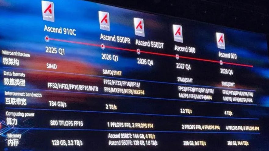
The Ascend series is the core of Huawei’s in-house AI computing platform, designed primarily for large-scale model training and inference. Since the launch of the Ascend 910 in 2019, Huawei has continuously iterated its lineup, introducing high-performance and energy-efficient chips such as Ascend 910C and the latest Ascend 920, supporting workloads across natural language processing, computer vision, and generative AI.
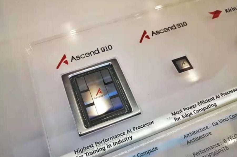
The Ascend 910C is built on a 7nm process and adopts a dual-die packaging architecture, integrating two 910B dies. It delivers approximately 800 TFLOPS of BF16 compute performance and 3.2 TB/s of memory bandwidth, with performance comparable to the NVIDIA H100. It is optimized to reduce model training time, particularly for generative AI and large language models such as PanGu and LLaMA.
The Ascend 920 represents the next-generation AI chip, manufactured using SMIC’s 6nm process. It supports HBM3 memory, achieving up to 900 TFLOPS BF16 performance and 4 TB/s memory bandwidth. The chip is optimized at the hardware level for Transformer architectures and sparse activation models such as Mixture of Experts (MoE), further reducing inference latency and improving training throughput.
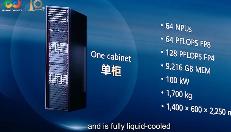
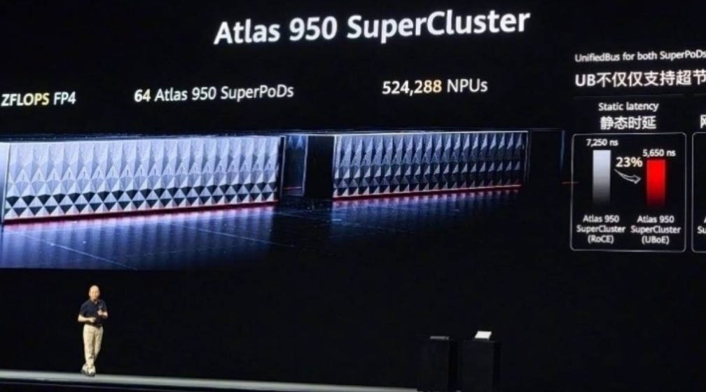
To support large-scale deployment, Huawei has also introduced the CloudMatrix 384 supernode, integrating 384 Ascend 910C chips and delivering up to 300 PFLOPS of compute performance. The system utilizes high-speed optical interconnects to minimize data transfer latency, making it suitable for training models with hundreds of billions of parameters. It has already been deployed in Huawei Cloud data centers and proprietary AI service platforms.
On the software side, Huawei promotes the MindSpore AI framework, deeply integrated with Ascend chips and supporting model conversion from TensorFlow and PyTorch. It also offers the ModelArts platform and Ascend AI Cloud, providing a full-stack toolchain—from training and tuning to deployment—aimed at building a self-sufficient AI ecosystem and reducing reliance on external supply chains.
Cambricon:Focuses on the development of AI accelerators, offering a range of chips for both cloud and edge applications.
Cambricon is a Chinese AI chip design company founded in 2016 and headquartered in Beijing. Since its inception, it has focused on designing AI processors for cloud servers, edge devices, and endpoints, following a strategy of “cloud-edge integration with hardware-software co-design.” Its product portfolio includes general-purpose AI chips, accelerator cards, and neural processor IP, widely used in smart cities, autonomous driving, and industrial vision.

In cloud computing, Cambricon has launched the MLU (Machine Learning Unit) series of high-performance AI accelerators, with the MLU370 as a flagship product. Built on a 7nm process, it integrates 39 billion transistors and delivers up to 256 TOPS (INT8), more than doubling the performance of its predecessor. It utilizes LPDDR5 memory, offering higher data throughput and energy efficiency compared to GDDR6, making it suitable for high-load scenarios such as AI training, inference, and vision processing.
For edge and industrial applications, Cambricon offers the MLU220 series, including modules such as MLU220-SOM and MLU220-M.2. These solutions feature lower power consumption and smaller form factors, making them ideal for real-time analytics in smart cameras, traffic sensing, and machine vision. For mobile and endpoint devices, Cambricon also provides lightweight neural processor IPs such as Cambricon-1M and Cambricon-1H, which have been widely integrated into domestic SoC platforms.
To support developers, Cambricon offers software platforms such as NeuWare and MagicMind, compatible with TensorFlow, PyTorch, and ONNX. These platforms enable model conversion, compilation, deployment, and optimization, helping developers efficiently run AI workloads on Cambricon hardware. The company has also partnered with multiple domestic data centers and cloud providers to deliver end-to-end AI computing solutions.
Cambricon maintains strong technological independence and commercialization capability in China and is actively expanding into global markets. Facing competition from players such as NVIDIA and Huawei Ascend, it continues to enhance its competitiveness through architectural innovation and process optimization.
Alibaba Group:Develops the Hanguang series of AI chips to support AI inference workloads in its cloud services.
Alibaba Group officially launched its first in-house AI chip, Hanguang 800, in 2019. It was jointly developed by Alibaba’s semiconductor arm, T-Head, and its DAMO Academy. The chip is designed specifically for cloud-based AI inference workloads, aiming to improve processing speed and energy efficiency while optimizing internal operations such as e-commerce and cloud services. The launch of Hanguang 800 marked a major step in Alibaba’s vertical integration of AI chips and data center infrastructure.
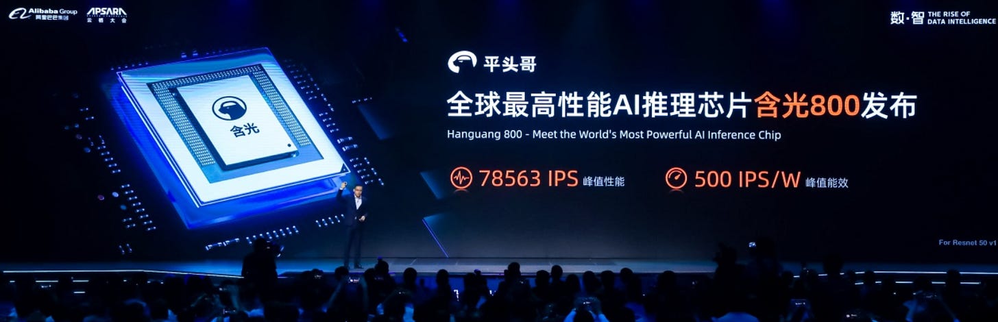
Hanguang 800 is built on TSMC’s 12nm process and integrates approximately 17 billion transistors, delivering peak performance of up to 820 TOPS. In ResNet-50 image classification tasks, it can process over 78,000 images per second, with energy efficiency reaching 500 images per second per watt—around 3–4× higher than mainstream chips at the time. The chip is optimized for low-latency, high-throughput inference tasks such as image search, speech recognition, and video understanding.
In real-world deployment, Hanguang 800 has been widely adopted across Alibaba’s core platforms, including Taobao. For example, Taobao’s image search service (“Pailitao”) processes over 1 billion product images daily; tasks that previously took hours can now be completed in just five minutes, significantly improving efficiency and user experience. The chip is also used in smart city applications such as Alibaba’s City Brain for real-time video analytics and traffic optimization.
To support cloud inference services, Alibaba integrates Hanguang 800 into its X-Dragon server architecture, providing bare-metal–level high-performance compute resources as part of Alibaba Cloud’s AI offerings. Developers and enterprises can deploy and run AI models on cloud instances powered by Hanguang 800, enabling rapid deployment of intelligent applications.
Looking ahead, Alibaba plans to expand the Hanguang series into additional domains, including medical imaging diagnostics, autonomous driving edge devices, and enterprise intelligent assistants. By vertically integrating chips, systems, and application services, Alibaba continues to strengthen its control over AI infrastructure and enhance its competitive position in the AI ecosystem.
Thanks for reading SEMIVISION @_@! This post is public so feel free to share it.


PreviousNext
TopLatestDiscussions








See all