3PHI: Building the Future of 3D-IC and Silicon Photonics Integration Ecosystem
3PHI: Building the Future of 3D-IC and Silicon Photonics Integration Ecosystem
- Source: SemiVision
- Author: SEMIVISION
- Published: 2026-04-02T10:29:01+08:00
- URL: https://tspasemiconductor.substack.com/p/3phi-building-the-future-of-3d-ic (1) 3PHI: Building the Future of 3D-IC and Silicon Photonics Integration Ecosystem


3PHI: Building the Future of 3D-IC and Silicon Photonics Integration Ecosystem
Original Article By SemiVision Research [Reading time: 16 mins]

Apr 02, 2026
∙ Paid

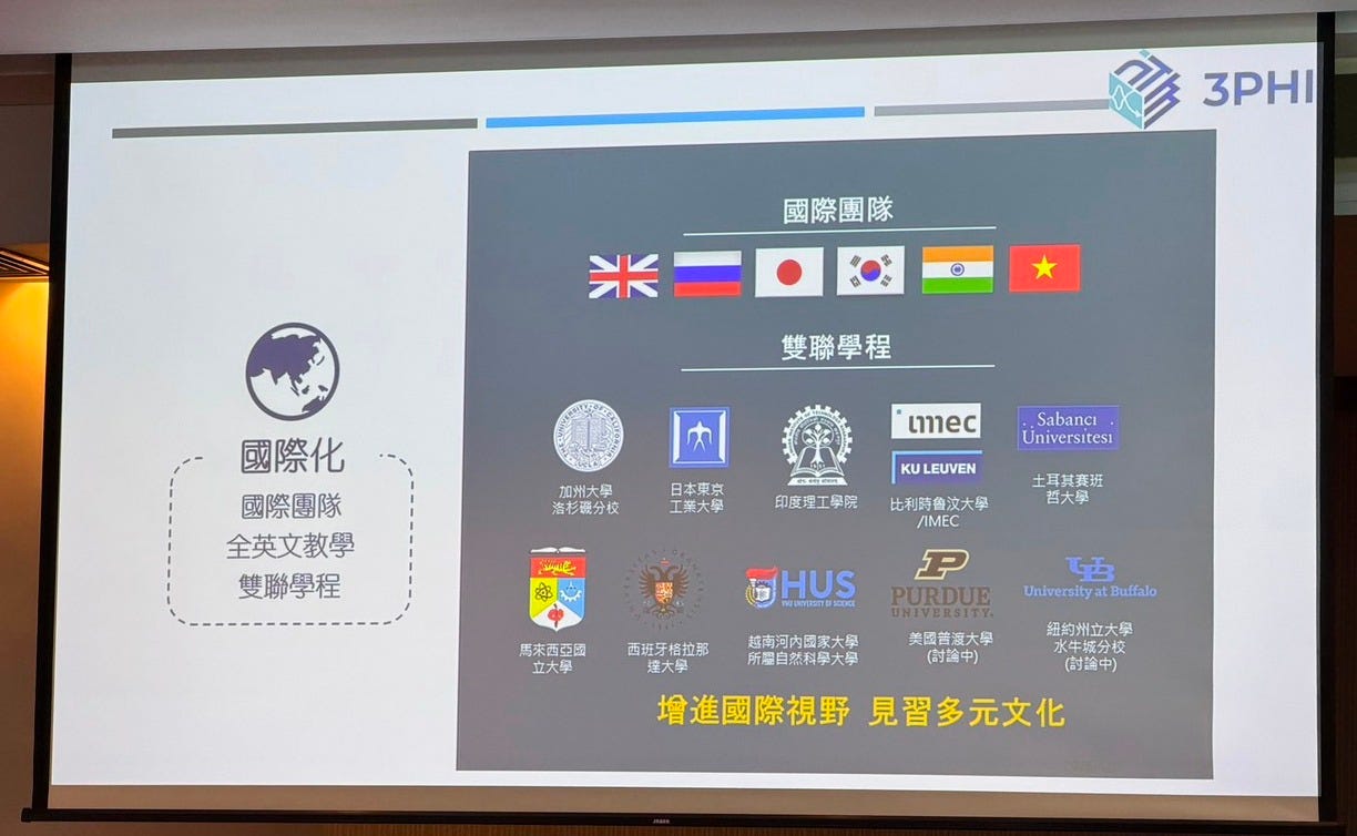
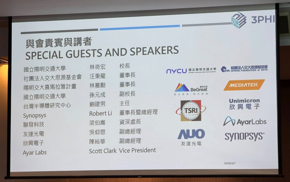
Today, SemiVision had the privilege of participating in the opening ceremony of the3D-IC & Si-Photonics Heterogeneous Integration Alliance (3PHI)in 2026. Initiated by National Yang Ming Chiao Tung University, the alliance aims to build a world-class platform that bridges academia and industry, focusing on 3D IC, co-packaged optics, and silicon photonics integration.

The alliance is designed to foster deep collaboration across the semiconductor value chain—from design, manufacturing, packaging, testing to system-level applications—while accelerating innovation through shared technologies and cross-disciplinary research. By integrating global academic and industrial resources, 3PHI seeks to strengthen Taiwan’s leadership in advanced process technologies and system integration.
Key missions include advancing 3D IC and optical co-packaging technologies, enabling next-generation R&D integration, providing technical consulting and technology transfer, cultivating long-term talent development, and promoting cross-domain innovation.
This marks an important milestone as heterogeneous integration and optical interconnects move from concept to large-scale deployment in AI infrastructure.
3PHI contact email: alli3phi@nycu.edu.tw
AI compute demand has grown explosively since 2012, with the FLOPS required to train large language models increasing by more than a billion-fold. However, the size of a single chip is constrained by the reticle limit (approximately 845 mm²), making it no longer feasible to scale performance simply by enlarging die size. At the same time, power consumption and thermal density of high-end AI/GPU chips are approaching physical limits, rendering single-package solutions insufficient.
As a result, heterogeneous integration has emerged as a key solution. By integrating multiple processors, memory, and optical components through advanced packaging, it becomes possible to overcome die size constraints while shortening signal transmission paths through close-proximity deployment.
As inter-chip data rates reach the TB/s scale, traditional copper interconnects and PCB traces suffer from severe attenuation and crosstalk. The energy cost of cross-chip communication can reach tens of picojoules per bit (pJ/bit). New interconnect paradigms must strike a balance between higher bandwidth and lower power consumption—bringing optical interconnects into the spotlight.
Optical signals, transmitted through fiber or waveguides, offer ultra-low loss and enable both long-distance and high-bandwidth communication. However, current optical engines—primarily composed of lasers and silicon photonic modulators—still face challenges in cost and power consumption. Emerging technologies such as fine-pitch photonics and microLED-based optical sources are beginning to reshape this landscape.
This analysis synthesizes the latest publicly available information to examine the strategies, technological evolution, and challenges of MediaTek, AUO, Ayar Labs, and Unimicron in the domains of heterogeneous integration and optical interconnects.
Key Technology Drivers and Shared Challenges
The Necessity of Chiplets and 3D Packaging
Due to reticle limitations, advanced nodes can no longer rely on monolithic scaling to increase compute performance. Instead, chiplet architectures are required to integrate compute dies with high-bandwidth memory (HBM). Common packaging approaches include CoWoS, fan-out, and 3D IC technologies.
Interconnect Bottlenecks Across Chips
Within AI servers, GPU-to-HBM bandwidth can easily reach several TB/s. Existing copper-based interconnects exhibit significant signal degradation and crosstalk over distances beyond a few centimeters, necessitating retimers and DSP compensation. This drives energy consumption to 10–20 pJ/bit. At system scale, interconnecting tens of thousands of ICs using conventional electrical links leads to a sharp decline in energy efficiency, becoming a critical bottleneck for large AI clusters.
Opportunities and Challenges of Optical Interconnects
Co-packaged optics (CPO), based on lasers and silicon photonic modulators, can deliver transmission speeds exceeding 800 Gbps. However, cost and power consumption remain key constraints. Fine-pitch photonics aims to further miniaturize lasers and modulators, integrating optical engines directly into packages while leveraging remote laser sources to reduce thermal load.
An alternative approach involves using large-scale microLED arrays to enable “slow-and-wide” parallel optical transmission. This architecture leverages the inherent advantages of microLEDs—high thermal tolerance, strong reliability, and lower cost—offering a potentially scalable path forward.

3月6日
Below we will share:
MediaTek: From Hybrid Electro-Optical Packaging to Active MicroLED Cable
AUO: Enabling “Slow-and-Wide” Optical Interconnects with MicroLED
Ayar Labs: UCIe Optical I/O Chiplets and Remote Laser Architecture
Unimicron: A Substrate Leader’s Strategy in Heterogeneous Integration
Trends and Outlook
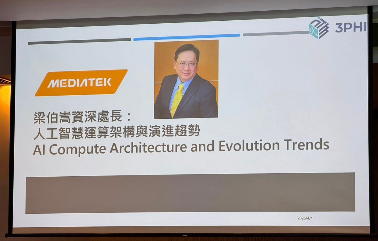
MediaTek: From Hybrid Electro-Optical Packaging to Active MicroLED Cable
AI Interconnect Bottlenecks and Heterogeneous Integration
MediaTek believes that the explosive growth of AI model scale is the primary driver behind heterogeneous integration and optical interconnects. The company points out that die size limitations make it necessary to build compute modules by stacking multiple compute dies and HBM memory using chiplet architectures.
MediaTek’s advanced packaging platform integrates 2.5D/3D IC technologies with its in-house SerDes, while collaborating with OSAT partners to adopt packaging solutions such as CoWoS and fan-out.
Co-Packaged Optics (CPO) Platform and Hybrid Electro-Optical Approach
At OFC 2024, MediaTek showcased a next-generation ASIC platform integrated with the Odin optical engine from Ranovus. This platform integrates 8 × 800 Gbps electrical links and 8 × 800 Gbps optical links on a single ASIC, delivering up to 12.8 Tbps of total bandwidth within the same board footprint.
This hybrid architecture uses SerDes for short-reach electrical transmission while leveraging CPO at the board edge for optical output, achieving an estimated system power reduction of around 50%. MediaTek emphasized that its 3 nm design capabilities and advanced packaging technologies enable tight integration of optical engines, ASICs, and HBM within a single package—optimizing both compute and interconnect simultaneously.
At the 2024 OCP Global Summit, MediaTek also introduced its 224 Gbps long-reach SerDes and highlighted its compatibility with CPO optical engines, forming a heterogeneous “electrical + optical” I/O architecture on the same ASIC.
Furthermore, MediaTek noted in a 2025 interview that the company currently prioritizes hybrid solutions—leveraging the coexistence of silicon photonics and SerDes to extend the lifecycle of copper interconnects until their physical limits are reached. Fully optical solutions are not yet the immediate priority.
He also mentioned that MediaTek is developing 336 Gbps SerDes to support higher bandwidth demands, while emphasizing that thermal management and cooling remain central challenges in advanced packaging design.

2月24日
Active MicroLED Cable: An Innovative Optical Interconnect Introduced with Microsoft
In March 2026, MediaTek and Microsoft Research jointly introduced the Active MicroLED Cable, a novel data center interconnect technology. This optical cable replaces a single laser source with hundreds of microLEDs. While each channel operates at only 2–3 Gbps, massive parallel arrays enable scaling to Tbps-level aggregate bandwidth—eliminating the need for complex SerDes and DSP.

Key Features and Technical Insights
~50% Lower Power Consumption
MicroLED arrays can be directly integrated with CMOS drivers, removing the need for power-hungry DSP. This reduces total system power consumption by approximately half compared to laser-based solutions.
High Reliability and Longevity
MicroLEDs exhibit strong tolerance to high temperature and current, with significantly longer lifetimes than traditional lasers. As a result, the solution is described as achieving “copper-like” reliability.
Extended Reach
The technology supports transmission distances exceeding 2 meters while maintaining low energy consumption, outperforming conventional copper cables.
Scalability
Total bandwidth can be scaled linearly by increasing the number of microLED channels or boosting per-channel data rates. Monolithic CMOS integration further enables direct bonding of microLED arrays and photodiodes onto a single chip.
The introduction of Active MicroLED Cable signals that MediaTek is actively exploring alternative light sources beyond lasers. The success of this approach depends on large-scale heterogeneous integration across microLED packaging, waveguide coupling, and driver ICs. Looking ahead, this technology could be deployed in short-reach, high-density intra-rack (scale-up) connections, and potentially expand to inter-rack (scale-out) and even cross–data center (scale-cross) applications.

3月20日
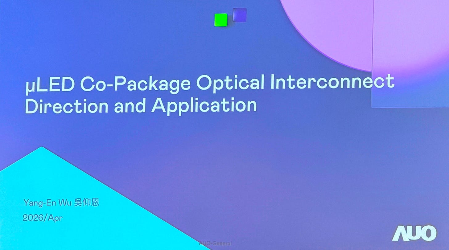
AUO: Enabling “Slow-and-Wide” Optical Interconnects with MicroLED
MicroLED CPO Modules and Data Center Applications
AUO has over a decade of experience in the display industry, particularly in large-scale MicroLED array packaging and driver integration. In recent years, organizations such as TrendForce and Optica have noted that AUO is extending its microLED technology into the optical interconnect domain, introducing commercially viable MicroLED-based co-packaged optics (CPO) modules.
These modules are designed to replace copper cables or short-reach laser modules within server racks (typically under 1 meter), reducing power consumption while improving reliability. MicroLED CPO solutions can consume as little as 5% of the power of copper interconnects, with energy efficiency reaching approximately 1–2 pJ/bit—making them highly attractive for AI data centers.
A report from April 2026 indicates that AUO is preparing to commercialize these MicroLED CPO modules for high-performance AI server racks. Analysts highlight that the “slow-and-wide” architecture enables Tbps-level bandwidth without requiring complex serializers/deserializers (SerDes), while achieving up to 95% power savings. Additionally, MicroLED modules can be co-packaged with CMOS drivers on the same substrate, and their high thermal tolerance allows deployment directly on server motherboards or substrates, reducing cooling costs.
“Slow-and-Wide” Architecture and Bandwidth Density
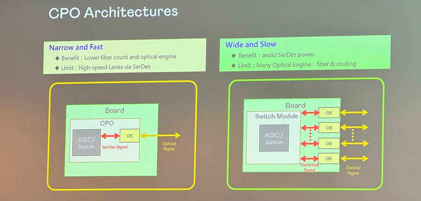
The core concept behind MicroLED optical interconnects is to achieve high aggregate bandwidth by operating a large number of low-speed channels in parallel. According to Optica, each MicroLED emitter typically operates at around 3 Gbps, but hundreds or even thousands of emitters can be integrated within a single package, enabling total bandwidth in the hundreds of Gbps to Tbps range.
Each emitter runs at relatively low clock frequencies (hundreds of MHz), with energy consumption per bit below 2 pJ—significantly lower than laser-based or SerDes-driven solutions. LEDinside further notes that MicroLED interconnects can achieve extremely high bandwidth density, as bandwidth scales linearly with channel count without the need for complex serialization or DSP.
Beyond density advantages, MicroLEDs offer superior tolerance to high temperature and current compared to semiconductor lasers. This eliminates the need for costly thermal management during packaging and operation. Optica reports that MicroLED arrays are already used in automotive headlights and displays, demonstrating high reliability and operation at temperatures exceeding 150 °C.
AUO leverages this experience by applying monolithic CMOS integration techniques, directly bonding MicroLED arrays and photodiodes onto silicon substrates to achieve ultra-high-density optical I/O. Current technical challenges include improving waveguide coupling efficiency and packaging precision. It is expected that MicroLED interconnects will first be deployed in chiplet-to-chiplet connections, before scaling to intra-rack and inter-rack applications.
Application Scenarios and Outlook
MicroLED CPO primarily targets short-reach (<10 meters), high-bandwidth-density applications. Typical use cases include interconnects between GPUs within AI servers, links between GPUs and HBM memory, and advanced automotive electronic systems.
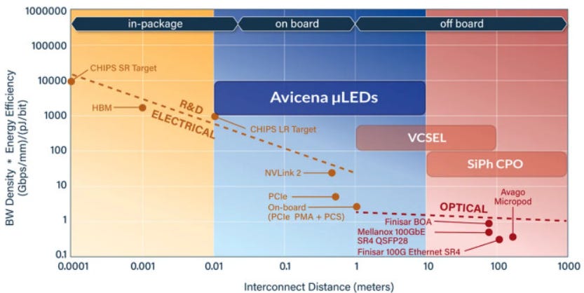
Industry report points out that, due to the absence of retimers and DSP, MicroLED CPO can also be applied in automotive sensing and defense systems. LEDinside suggests that while MicroLED optical interconnects are still in an early stage—facing challenges in waveguide coupling, micron-level alignment, and long-term reliability—they are expected to become a key technology for short-reach optical connectivity by 2030 as costs decline and manufacturing scales improve.
Ayar Labs: UCIe Optical I/O Chiplets and Remote Laser Architecture
TeraPHY and SuperNova

Ayar Labs is an early pioneer in silicon photonics-based optical I/O, focusing on optical I/O chiplets and remote laser light sources. Its flagship product,TeraPHY, is a compact, low-power, and low-latency optical I/O chip designed using standard CMOS combined with silicon photonics processes. It is compliant with the UCIe standard and can function as a chiplet interconnected with CPU, GPU, and HBM within advanced packages.
According to official data, the third-generation TeraPHY provides 8 full-duplex optical ports per chiplet, with each port supporting 16 WDM wavelengths, delivering up to 8 Tbps of bidirectional bandwidth. Latency per chiplet is approximately 10 ns, with communication distances ranging from millimeters to kilometers.
When paired with the SuperNova remote laser module, the system can achieve 5–10× bandwidth improvement, 10× lower latency, and 4–8× better energy efficiency. SuperNova consists of distributed feedback (DFB) lasers located remotely, supplying optical signals to TeraPHY chiplets.
Industry interviews indicate that third-generation TeraPHY can transmit UCIe protocols optically, enabling chiplets such as GPUs and HBM to communicate over fiber as if they were within the same package. Each optical port uses 16 microring resonators for wavelength selection, achieving ~1 Tbps per port. SuperNova modules can support 8 or 16 ports, each generating 16 wavelengths.
Eliminating Electrical SerDes and Creating Optical “Islands”
Unlike traditional CPO architectures, Ayar Labs’ TeraPHY eliminates electrical SerDes entirely. Optical I/O is integrated directly at the die level, removing the need for power-intensive SerDes and DSP blocks between GPUs.
This architecture enables the formation of “optical islands,” where GPUs across different boards or servers are interconnected optically and behave as if they reside within the same package. Such a paradigm allows thousands of GPUs to operate cohesively, addressing the scalability demands of large AI model training clusters.
Ayar Labs believes that once manufacturing and testing bottlenecks are resolved, optical I/O will enable seamless, scalable compute fabrics spanning distances from millimeters to kilometers.
The third-generation TeraPHY is currently built on GlobalFoundries 45 nm silicon photonics technology, but the company has indicated portability to other foundries such as TSMC, along with integration into 2.5D/3D advanced packaging platforms. By adhering to the UCIe standard, TeraPHY enables standardized optical interconnects across chiplet ecosystems.
Ayar Labs is also heavily investing in wafer-level testing to ensure Known Good Die (KGD), which is critical as customers integrate multiple TeraPHY chiplets within a single package to build ultra-high-bandwidth channels. High yield and reliability at the wafer level are essential to overall system performance.
Manufacturing and Testing Challenges
Ayar Labs emphasizes that the bottleneck for large-scale optical I/O deployment is not just the core technology, but also the surrounding ecosystem—including fiber attach, waveguide integration, and testing infrastructure.
A 2025 blog post highlights the importance of developing pluggable optical connectors in collaboration with partners. Examples include glass photonic interconnects from Intel Foundry and the TeraVERSE connector from Teramount.
Another discussion on CPO mass production strategies points out that success depends on a unified OSAT ecosystem and extensive testing capacity. Manufacturing facilities must support high-density optical alignment and connector assembly at scale. Standardization itself is not the primary challenge—rather, supply chain readiness and testing infrastructure are the true keys to scaling deployment.
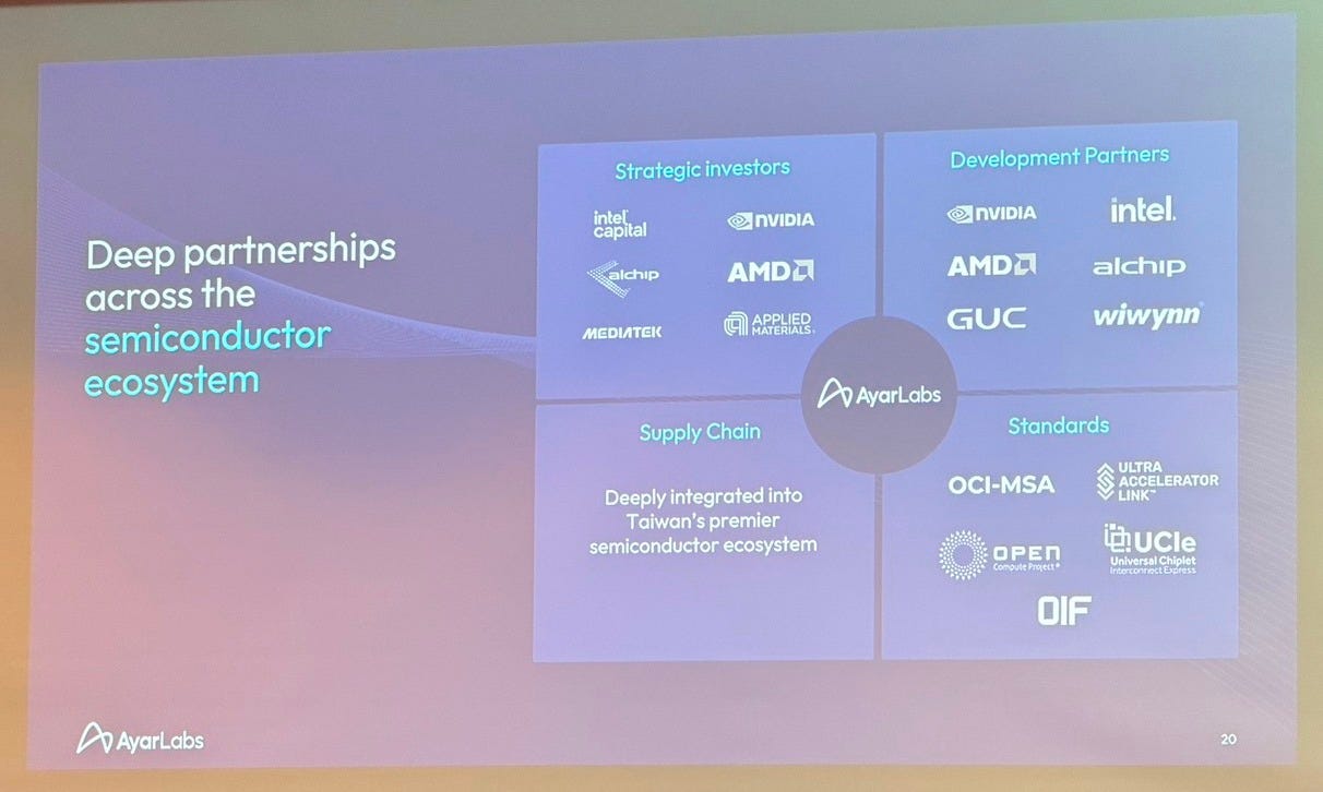
This aligns with Ayar Labs’ broader strategy: building deep partnerships across the ecosystem, including foundries (GlobalFoundries, TSMC), packaging providers (such as ASE and GUC), and test equipment vendors, to secure a strong position within the heterogeneous integration landscape.
Unimicron: A Substrate Leader’s Strategy in Heterogeneous Integration
ABF Substrates and Chiplet Architecture
Unimicron is a global leader in ABF substrates, long supplying advanced packaging substrates to companies such as AMD and NVIDIA. As AI chips evolve from monolithic designs to chiplet-based multi-die stacking, substrate sizes have expanded from around 100 × 100 mm to 120 × 120 mm, while layer counts have increased from roughly 20 layers to 30 or even up to 78 layers in advanced PCBs.
Unimicron emphasizes that substrates serve as the “foundation” of the system, supporting increasingly complex 3D IC stacks. Key challenges in heterogeneous integration include coefficient of thermal expansion (CTE) mismatch, structural warpage, and signal integrity (SI/PI) management. These issues require close co-design collaboration with chip designers to mitigate thermal and mechanical stress.

Driven by AI demand, Unimicron continues to expand ABF capacity. A 2026 Yahoo Finance report indicates that the company plans to invest approximately NT$254 billion in capital expenditures, expanding ABF production lines in Taiwan (Guangfu Phase II) and a new facility in Thailand to meet AI and high-performance computing demand.
At the same time, Unimicron participates in the 3DIC Advanced Manufacturing Alliance (3DICAMA) at SEMICON Taiwan—co-led by TSMC and ASE Technology—aiming to build a comprehensive 3D IC advanced packaging ecosystem and overcome bottlenecks in thermal management and interconnect scaling.
Perspectives on Optical Interconnects and New Materials
As a substrate supplier, Unimicron’s role is to provide platforms compatible with optoelectronic integration. The company recognizes that optical-electrical integration imposes stricter requirements on substrate flatness and dimensional stability, while also introducing challenges in managing mechanical stress from embedded waveguides or optical fibers within PCBs.
Regarding glass substrates, Unimicron maintains a cautious stance. According to technical analysis from 3DInCites, simulations conducted by Unimicron engineers show that while glass-core substrates have CTE values close to silicon, flip-chip connections on glass result in 3–4× higher inelastic strain at solder joints compared to organic substrates, increasing the risk of cracking. The study suggests tuning glass CTE to better match PCB materials and concludes that glass substrates are likely to remain limited to niche applications in the near term.

2025年6月30日
Glass substrates offer advantages such as low dielectric constant (Dk) and CTE values of 3–7 ppm/°C—close to silicon—making them suitable for embedding optical waveguides and enabling Cu–Cu hybrid bonding. However, costs are currently 3–5× higher than traditional ABF substrates, and yield and reliability remain unproven. Large-scale adoption is unlikely before 2028.
Unimicron is evaluating glass substrate technologies in alignment with TSMC’s roadmap, with validation expected to begin in 2026 and mass production requiring an additional 12–24 months. While glass substrates are unlikely to replace ABF in the short term, they hold long-term potential for deep integration with optical interconnects.
Ecosystem and Collaboration
Unimicron emphasizes that substrate technology must be co-developed with foundries, packaging houses, and system vendors to meet the demands of chiplet integration and optical interconnects. The company actively participates in 3DICAMA and multiple industry standard organizations, collaborating with TSMC and ASE to define interface standards between substrates and optoelectronic components.
Additionally, Unimicron works with material suppliers and equipment partners to develop low-CTE resins, low-Dk dielectric materials, and high-density via technologies—laying the groundwork for future platforms such as CoWoS, panel-level packaging (PLP), and CPO solutions.

2025年5月12日
Trends and Outlook
AI-driven connectivity demand is accelerating electro-optical integration
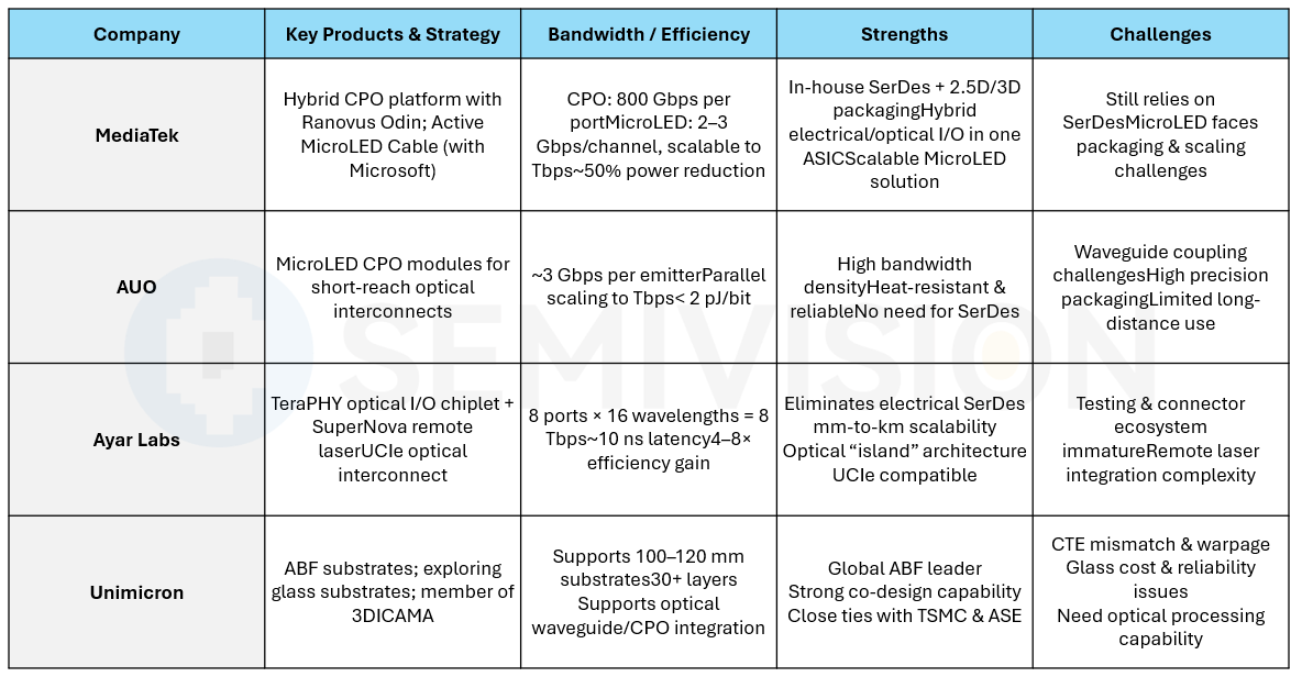
The scale of AI models continues to double year by year, requiring GPUs to exchange massive amounts of parameters through high-speed, low-latency interconnects. Whether it is MediaTek’s hybrid CPO approach, Ayar Labs’ full optical I/O, or AUO’s MicroLED-based CPO, all aim to reduce power consumption, expand bandwidth, and minimize latency.
In the near term, hybrid solutions are more practical as they coexist with existing SerDes technologies. In the long run, however, fully optical interconnects—enabled by standards such as UCIe—are expected to eliminate the bottlenecks of electrical SerDes.
MicroLED and silicon photonics are complementary
MicroLED emphasizes a “slow-and-wide” parallel architecture, making it well-suited for short-reach, high-density interconnects. In contrast, silicon photonics leverages high-speed modulation and wavelength-division multiplexing (WDM), making it ideal for medium- to long-distance links, including rack-to-rack and beyond.
Future data centers are likely to adopt both approaches: MicroLED for intra-package or board-level short-reach communication, and silicon photonics for longer-distance or cross-node interconnects.
The critical role of advanced packaging and substrates
As both optical interconnects and chiplet stacking evolve, substrates and packaging must support increasingly diverse components. Suppliers like Unimicron need to address challenges such as CTE mismatch, warpage, and signal integrity, while developing low-Dk materials and exploring glass substrates.
Substrate vendors must collaborate closely with foundries and OSATs to establish co-design frameworks that support optical I/O integration. While glass substrates hold long-term potential, ABF substrates will remain dominant in the near term.
Ecosystem development and standardization
Ayar Labs emphasizes the importance of remote light sources, pluggable optical connectors, and scalable testing infrastructure. MediaTek and AUO similarly depend on supply chain maturity in microLED packaging and waveguide integration.
The industry is moving toward ecosystem-driven collaboration, involving foundries, OSATs, substrate vendors, optical component suppliers, and system companies. Alliances such as SEMI’s 3DICAMA are emerging to define standards, share infrastructure, and accelerate the adoption of CPO and optical I/O technologies.
Conclusion
Heterogeneous integration and optical interconnects are becoming foundational to next-generation AI and high-performance computing architectures. MediaTek is advancing through hybrid CPO while exploring MicroLED cables; AUO is pushing short-reach optical connectivity via MicroLED CPO; Ayar Labs advocates fully optical I/O to enable scalable “optical islands”; and Unimicron, as a substrate leader, is building the foundation to support these innovations.
No single solution will dominate. Instead, these approaches will coexist and complement each other across different distance and power requirements. As standards like UCIe mature, testing and packaging infrastructure improves, and ecosystem collaboration deepens, the heterogeneous integration and optical interconnect landscape will continue to expand—delivering higher energy efficiency and scalability for the next wave of AI computing.
Thanks for reading SEMIVISION @_@! This post is public so feel free to share it.

2025年6月13日


PreviousNext
TopLatestDiscussions








See all