SRAM as the New Compute Fabric: A Comparative Architecture Study of Groq LPU, Cerebras WSE, and Google TPU
SRAM as the New Compute Fabric: A Comparative Architecture Study of Groq LPU, Cerebras WSE, and Google TPU
- Source: SemiVision
- Author: SEMIVISION
- Published: 2026-03-30T20:47:43+08:00
- URL: https://tspasemiconductor.substack.com/p/sram-as-the-new-compute-fabric-a (1) SRAM as the New Compute Fabric: A Comparative Architecture Study of Groq LPU, Cerebras WSE, and Google TPU


SRAM as the New Compute Fabric: A Comparative Architecture Study of Groq LPU, Cerebras WSE, and Google TPU
Original Article By SemiVision Research [Reading time: 22 mins]

Mar 30, 2026
∙ Paid
The New Bottleneck in AI Inference
Over the past few years, large language models (LLMs) and generative AI agents have advanced rapidly. As a result, inference speed and energy efficiency have become critical factors shaping user experience.
In 2026—particularly in major Asian technology hubs such as Taipei—user expectations for chatbots, voice assistants, real-time translation, and autonomous agents continue to rise. The industry now faces a shared challenge: how to reduce the time required to generate each token while maintaining model accuracy.
Traditional GPU architectures are optimized for floating-point computation and high throughput. However, during inference—especially in the decode stage—models repeatedly access intermediate results from previous layers. This creates a new bottleneck:memory access latency and bandwidth.

3月17日
To address this challenge, NVIDIA, together with SRAM-centric accelerator company Groq, has introduced a new architecture: the Language Processing Unit (LPU). Built around ultra-high-bandwidth on-chip SRAM, and integrated into a heterogeneous platform such asVera Rubin + LPX, this approach is designed to significantly reduce LLM inference latency.
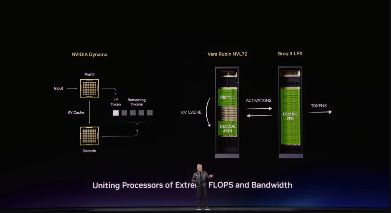
This article, based on multiple official reports and industry analyses, examines the advantages of SRAM in inference from three perspectives: physical fundamentals, architectural design, and industry strategy—while exploring the future role of LPU in AI computing systems.
Memory Types and Trade-offs: SRAM, DRAM, and HBM

Before understanding the LPU architecture, it is essential to clarify the characteristics of different memory technologies.
Dynamic Random-Access Memory (DRAM)is the dominant memory used in today’s servers and GPUs. Each DRAM bit consists of one transistor and one capacitor, with the capacitor storing charge to represent binary states. This design allows for high density and scalability. However, because capacitors leak charge, DRAM requires periodic refresh cycles and suffers from relatively slow access speeds.
In contrast,Static Random-Access Memory (SRAM)uses six transistors to form two cross-coupled inverters. The stored data is maintained through stable voltage states, eliminating the need for refresh. According to Gimlet Labs, SRAM cells achieve access times of around 1 ns, whereas DRAM cells typically require 10–15 ns.
SRAM can be co-located with compute units on the same silicon process, enabling extremely low latency and high bandwidth. However, its drawbacks include significantly larger area and higher cost per bit.
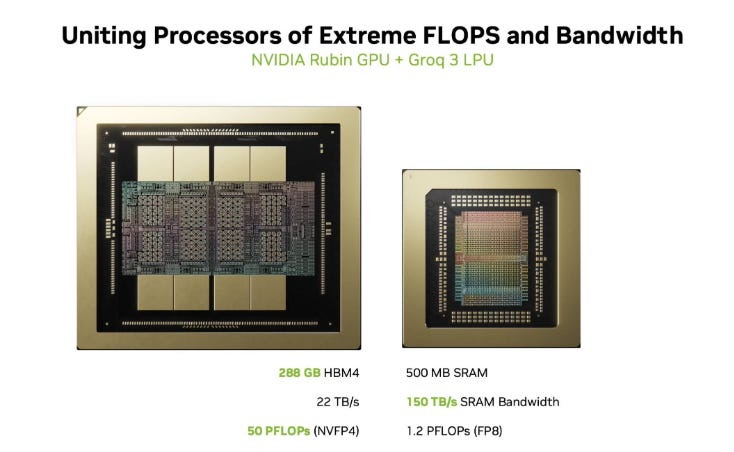
High Bandwidth Memory (HBM), designed for high-performance GPUs, stacks multiple DRAM dies using a silicon interposer to achieve massive aggregate bandwidth. For example, Rubin GPUs equipped with 288 GB of HBM4 can deliver up to 22 TB/s of bandwidth.
Despite this, HBM remains an off-chip DRAM solution. It connects to GPUs via 2.5D interposers and incurs latency from row activation and precharge operations. Typical access latency ranges from 375 to 500 ns, making it unsuitable for ultra-low-latency inference loops.
Within GPUs themselves, SRAM is already heavily utilized across the memory hierarchy. For instance, each SM in an H100 GPU includes 256 KB of register files and shared memory, with access latency below 1 ns. L1/L2 caches (also SRAM-based) have latencies around 20 ns, while external HBM3 access latency extends to hundreds of nanoseconds.
This establishes a clear Pareto frontier:
SRAM→ low capacity, ultra-fast
DRAM/HBM→ high capacity, slower access
The LPU architecture pushes this trade-off to the extreme—allocating a large portion of chip area to SRAM to achieve ultra-high bandwidth and ultra-low latency.

2025年10月13日
The Inference Bottleneck: Latency-Driven Workloads and Arithmetic Intensity
The inference process of large language models can be broadly divided into two stages:
Prefill
Decode
During the prefill stage, user inputs are vectorized and processed through matrix multiplications to establish relationships between context and model weights. This stage has high arithmetic intensity and is well-suited for GPUs, which excel at parallel computation.
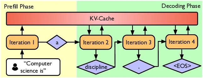
Prefill and decoding phase in the LLM inference
The decode stage, however, is fundamentally different. It generates tokens sequentially, relying on previous outputs at every step. The computation alternates between attention mechanisms and feed-forward networks (FFN/MoE), requiring continuous access to intermediate results.
This creates a workload that is:
Highly sequential (strong dependency across tokens)
Memory-intensive
Each token depends on the completion of the previous one, making large-scale parallelization difficult. Industry analysis shows that if a single step incurs an additional 10 ns latency, a 100-layer model would accumulate 1 μs delay—a significant impact for real-time applications.
The ratio between compute operations and memory access is known as arithmetic intensity. According to Gimlet Labs, workloads with low arithmetic intensity—such as sparse matrix operations in FFN/MoE—often become memory-bound. In such cases, compute units remain underutilized while waiting for data.
This is precisely where the LPU architecture differentiates itself. Rather than maximizing raw compute throughput, it prioritizes:
Extremely high SRAM bandwidth
Deterministic, low-latency data access
By trading off some compute density for memory efficiency, LPU targets the true bottleneck of modern inference workloads.
LPU Architecture Deep Dive: Massive SRAM and Deterministic Execution
Massive On-Chip SRAM and 150 TB/s Bandwidth
The NVIDIA Groq 3 LPU is fabricated on Samsung’s 4 nm process and integrates 512 MB of SRAM on a single die. According to current reports, this chip delivers 150 TB/s of memory bandwidth—an order of magnitude higher than the 22 TB/s provided by 288 GB of HBM4 in Rubin GPUs.
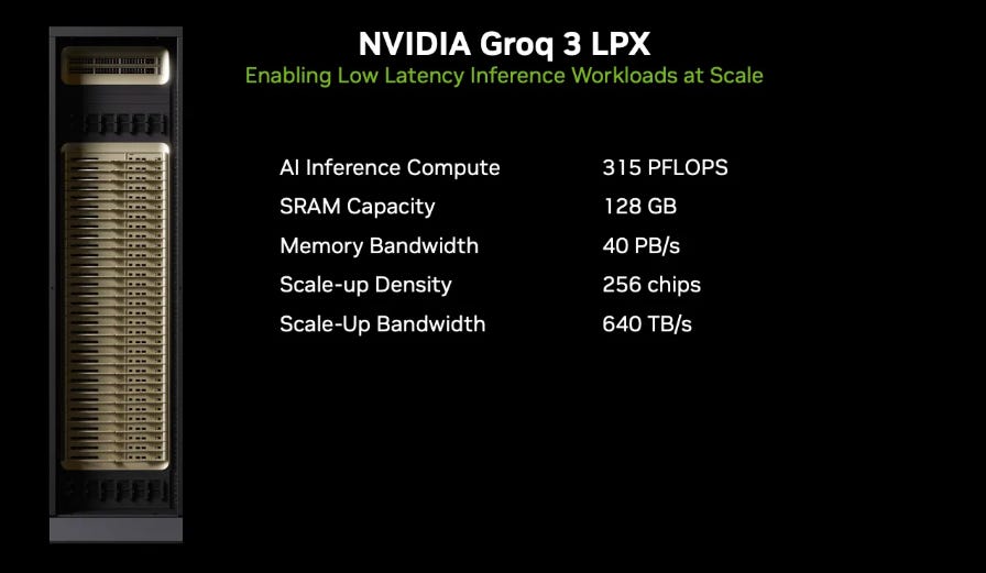
An LPX rack consists of 256 LPUs, collectively offering 128 GB of SRAM and an aggregate bandwidth of 40 PB/s. The high bandwidth of the LPU primarily comes from massive parallelism across numerous memory banks and on-chip interconnects, enabling extremely low read/write latency. This allows token generation throughput to scale from roughly 100 tokens per second to over 1,500 tokens per second.
Importantly, this bandwidth is not derived from a single memory bus, but rather from the aggregate performance of all SRAM banks. A single LPU may contain thousands of independent memory banks, each providing a width of 256 bytes. Operating at a 1.5 GHz clock frequency, these banks can simultaneously transfer data, resulting in aggregate bandwidth in the hundreds of TB/s.
Unlike DRAM, SRAM does not require row activation or precharge operations. Each bank can independently deliver data at every clock cycle, enabling consistent, low-latency access.
Earlier versions, such as LPU v1, featured 230 MB of SRAM, while the new LP30 increases this to 512 MB and introduces FP8 compute capability reaching 1.23 PFLOPS.
This design maximizes bandwidth density—delivering significantly higher instantaneous bandwidth per unit silicon area compared to GPUs—albeit at the cost of reduced total DRAM capacity.
Spatial Execution Model and Deterministic Scheduling
The LPU adopts aVLIW (Very Long Instruction Word) architecture combined with compiler-driven scheduling, forming a spatial execution model.
Unlike traditional GPUs, which rely on hardware schedulers for dynamic task dispatch, the LPU determines instruction scheduling entirely at compile time. As highlighted by ServeTheHome, Groq’s architecture uses the compiler to pre-arrange both computation and data movement paths.
As a result:
The hardware does not need to predict when data will arrive
Execution is not stalled by cache misses
All data transfers, computations, and synchronizations are predetermined per clock cycle
This deterministic execution model eliminates the jitter associated with cache misses in conventional GPU architectures and delivers highly stable tail latency, which is critical for real-time inference workloads.

CISC, RISC, and VLIW represent three distinct philosophies in processor design, each optimizing a different balance between hardware complexity, compiler responsibility, and execution efficiency.
CISC emphasizes rich, complex instructions to reduce software burden, but at the cost of more intricate hardware and less predictable performance.
RISC simplifies instructions and standardizes formats, enabling efficient pipelining and higher clock speeds while shifting some complexity to software.
VLIW goes one step further by delegating most scheduling and parallelism extraction to the compiler, allowing hardware to remain simple while executing multiple independent operations simultaneously.
In modern high-performance systems—especially AI accelerators—VLIW-like approaches are increasingly relevant, as they enable deterministic execution and high throughput by tightly coordinating computation and data movement at compile time.
Structurally, the LPU consists of multiple superlanes, each containing:
Compute units
Instruction storage (Instr)
Memory blocks (MEM)
The MEM blocks within each superlane are mirrored by SRAM banks on both the east and west sides, enabling multi-directional data movement across the chip.
According to NVIDIA’s official blog, each MEM module integrates approximately 500 MB of high-speed SRAM, composed of numerous smaller SRAM banks. The compiler directly maps data to specific physical bank addresses, allowing precise control over data placement.
During scheduling, data is assigned to designated banks and moved according to predefined communication protocols—referred to as RealScale chip-to-chip (C2C) links. These links operate under fixed clock timing, ensuring deterministic data transfer across chips while eliminating clock drift.
This plesiochronous protocol ensures that an entire LPU cluster operates as a single, tightly coordinated system, rather than a collection of loosely synchronized processors.
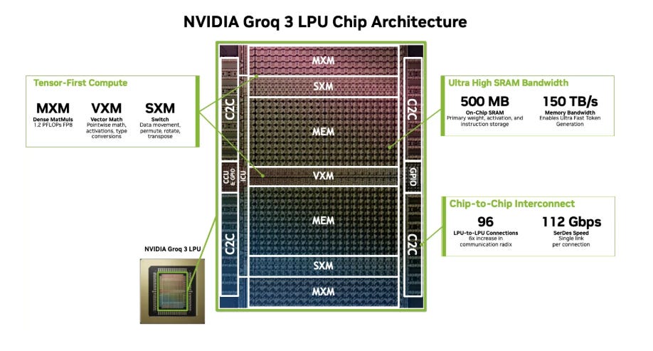
RealScale C2C Interconnect
LPU modules are interconnected via RealScale Chip-to-Chip (C2C) links. Each LPU is equipped with 96 C2C ports, operating at 112 Gbps per link, connecting to neighboring LPUs or BlueField DPUs to form a unidirectional point-to-point network.
Based on current understanding, each LPU delivers approximately 2.5 TB/s of inter-chip bandwidth through C2C connections. An LPX compute tray (comprising 8 LPUs) can achieve around 20 TB/s of scale-up bandwidth via 96 C2C links.
The RealScale interconnect does not require hardware arbitration. Instead, routing is software-defined, ensuring that data arrives within a predetermined timing window. This design further reinforces the deterministic execution model of the LPU architecture.


AFD: Decode Disaggregation and Heterogeneous Inference
Another key feature of the LPU is its cooperative execution model with GPUs, usingAttention–FFN Disaggregation (AFD)to handle the decode stage.
According to NVIDIA’s official blog, the prefill and attention stages are compute-intensive and require large memory capacity, making them well-suited for execution on Rubin GPUs. In contrast, the feed-forward network (FFN) and sparse MoE expert computations involve frequent weight access and are therefore memory bandwidth-intensive, making them ideal for execution on LPUs.


Feb 2026
Within the AFD loop, the LPU receives intermediate activations from the GPU, performs FFN/MoE computations, and then sends the results back to the GPU for the next attention layer. This process repeats iteratively across layers.
The advantage of this division of labor is twofold:
GPUs can maintain high utilization without being stalled by serial decode dependencies
LPUs can execute FFN operations with ultra-low latency, shortening the overall inference loop
By decomposing the decode process into amulti-engine loop, NVIDIA preserves the general-purpose flexibility of GPUs while leveraging the low-latency strengths of LPUs.
According to market data, pairing an LPX rack with an NVL72 GPU system can deliver up to 35× higher inference throughput per megawatt compared to Blackwell NVL72 when running trillion-parameter models.

In addition, NVIDIA’s Dynamo scheduling system dynamically orchestrates the AFD loop between GPUs and LPUs, allocating workloads based on batch size and parallelism levels. Dynamo evaluates KV cache size and latency targets in advance to determine when to route workloads to the LPU, enabling KV-aware routing.
Through low-overhead data transfer and latency-oriented scheduling, Dynamo minimizes cross-tenant interference and maintains stable tail latency. This significantly improves the efficiency of agentic AI workflows, including multi-step inference, retrieval, and tool usage.
Samsung’s Advantage: 4 nm Process and Supply Chain Strategy
Stacking 512 MB of SRAM on a single ASIC while maintaining high yield is no trivial task. Samsung Semiconductor serves as the manufacturing partner for the LPU, responsible for wafer fabrication as well as part of the high-bandwidth memory supply chain.
The LPU is fabricated using Samsung’s 4 nm process. Initial production capacity was around 9,000 wafers per month, which has since increased to approximately 15,000 wafers, with yields exceeding 80%. Each wafer can produce roughly 65 LPU dies.
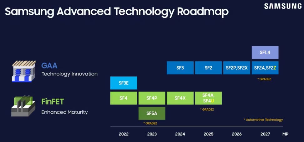
Due to the relatively large cell size of SRAM, a single wafer yields only about 60–70 dies, significantly fewer than GPU designs that rely on HBM. This is a key factor contributing to the higher cost of LPU chips.
However, as a global leader in DRAM, HBM, and logic foundry services, Samsung possesses a fully integrated memory and advanced packaging supply chain. Its strategy is to alleviate HBM supply bottlenecks by supporting alternative architectures such as the LPU.
The use of SRAM in LPUs is not intended to replace HBM. Instead, it acts as an offload engine for FFN/MoE workloads during decoding, allowing Rubin GPUs to avoid wasting precious HBM bandwidth on sparse computations.
System Integration: CPU, DPU, and DRAM Dependencies
In addition, each LPX compute tray includes a host CPU and a BlueField-4 DPU, responsible for operating system management and networking.
The BlueField-4 DPU integrates a 64-core Grace CPU, along with 128 GB of LPDDR5 memory and 114 MB of L3 cache. These components still require external DRAM modules. It is estimated that an LPX tray is equipped with approximately 384 GB of DDR5 DRAM (for example, six 64 GB RDIMMs), meaning the system as a whole continues to rely on DRAM.
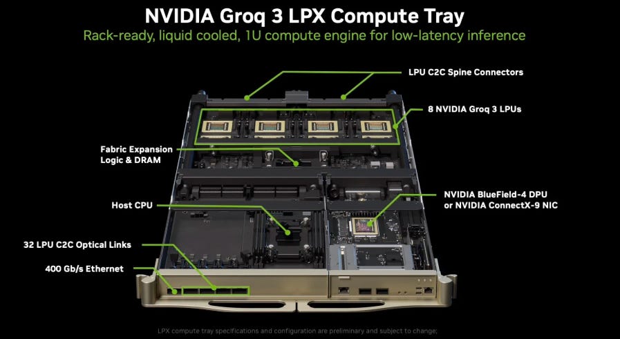
Samsung’s DDR5 supply also plays a critical role, further strengthening its supply chain position within the LPU + GPU heterogeneous platform.

3月2日
Heterogeneous Integration of Training and Inference
While the LPU demonstrates significant advantages in the decode stage of inference, model training still relies on GPUs.
This is because training involves backpropagation and gradient accumulation, requiring substantial computational throughput and memory capacity. Training workloads are typically optimized with large batch sizes to maximize hardware utilization.
Given the limited capacity of SRAM, it is not feasible to accommodate hundreds of gigabytes to terabytes of model weights and gradients. As a result, current LPU architectures are not suitable for training tasks.
In contrast, Rubin GPUs, equipped with a large number of Tensor Cores and HBM4, can deliver tens of TFLOPS to PFLOPS of training performance, while supporting low-precision formats such as FP8 and FP4.
The Future of Inference: Heterogeneous Architectures
For inference, the emerging trend isheterogeneous integration:
GPU→ Prefill and attention
LPU→ FFN / MoE
DPU→ Networking and security isolation
CPU→ Control and orchestration
A single LPX rack paired with an NVL72 GPU system can deliver the throughput required for state-of-the-art LLM inference, while achieving excellent performance per watt.
This architecture is expected to gradually replace GPU-only inference in cloud data centers, marking a transition toward a heterogeneous computing era.
Algorithm-Level Synergy: Speculative Decoding and Draft Models
To further reduce latency, researchers have introducedspeculative decoding.
This approach uses a lightweight draft model to generate a batch of candidate tokens in advance, which are then verified by a larger LLM. If the outputs are consistent, multiple tokens can be committed at once, significantly improving inference throughput.
According to NVIDIA’s official blog, the LPU’s deterministic execution model and ultra-high on-chip bandwidth make it particularly well-suited to act as a draft model engine, pre-generating tokens efficiently.
Meanwhile, the GPU continues to handle attention and validation tasks for the large model. This division of labor reduces bottlenecks within multi-stage inference loops.
In addition, researchers are exploring the integration of small specialized models within LLM pipelines. For example, compact models trained to predict classical text patterns or common phrases could be executed directly on the LPU, reducing the need to load large model parameters and further lowering computational overhead.
Economic and Industry Implications of Inference Architectures
Supply Chain and Market Competition
Over the past two years, the true bottleneck in the AI industry has not been wafer capacity, but rather HBM supply and advanced packaging capacity.
HBM demand is surging, yet only a handful of suppliers globally can deliver high-yield HBM dies and 2.5D interposer packaging at scale. The Groq 3 LPU, by leveraging an SRAM-centric design, effectively bypasses the HBM bottleneck and creates new growth opportunities for memory vendors such as Samsung.

The LPU solution does not rely on scarce HBM or still-maturing technologies like GDDR7, helping to alleviate pressure across the supply chain.

Source: SK Hynix
Industry Dynamics and Competitive Landscape
On the industry front, NVIDIA secured a non-exclusive license to Groq’s core technologies in 2025 for approximately $20 billion, enabling it to rapidly bring LPU products to market and integrate them into its Vera Rubin platform.
According to industry analysis, this move is analogous to NVIDIA’s 2019 acquisition of Mellanox, which established NVLink and InfiniBand as foundational technologies for AI infrastructure.
With the introduction of LPU as a dedicated inference accelerator, NVIDIA expands its value capture beyond training GPUs and positions itself to dominate the inference market as well.
At the same time, major cloud providers—including Google (TPU v7 Ironwood), Meta (MTIA), AWS (Trainium / Inferentia), and Alibaba (Zhenwu 810E)—are accelerating the development of their own inference ASICs.
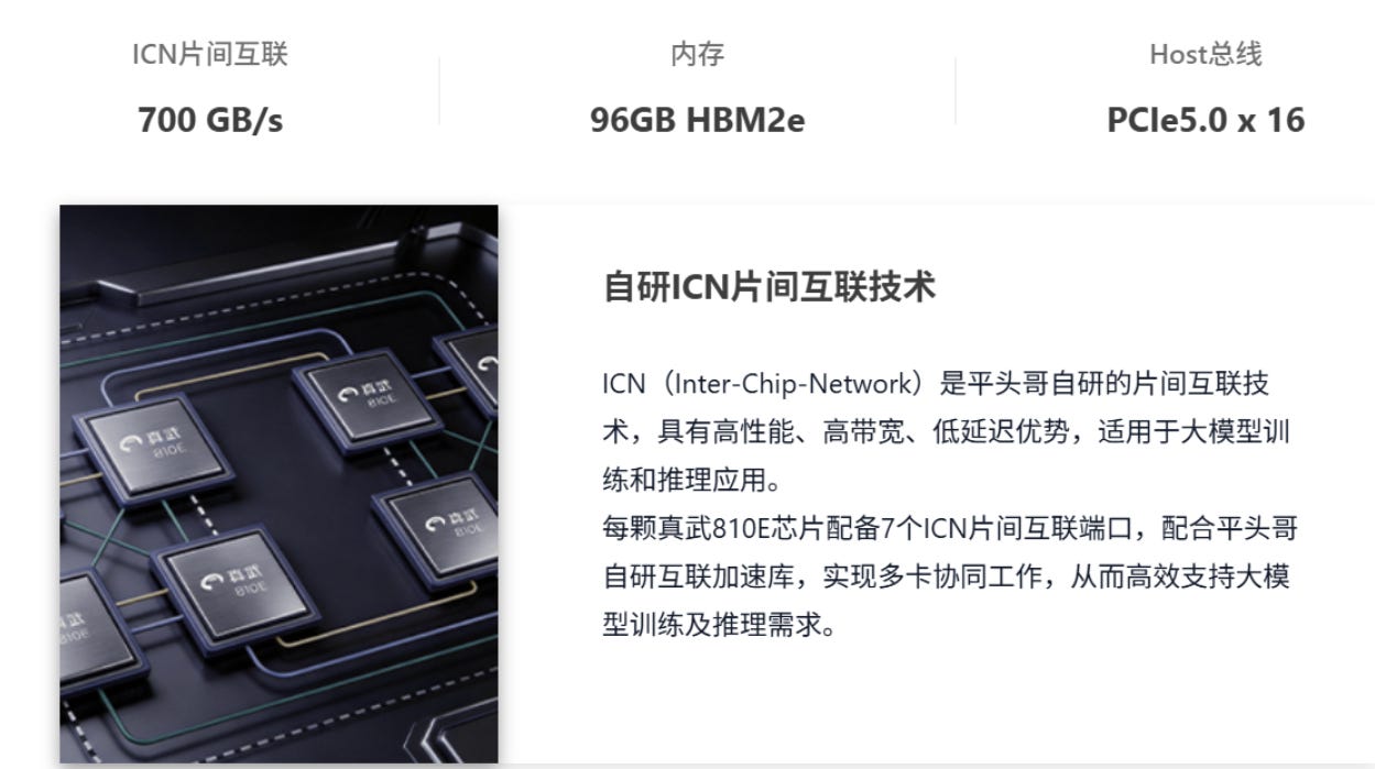
Alibaba (Zhenwu 810E)
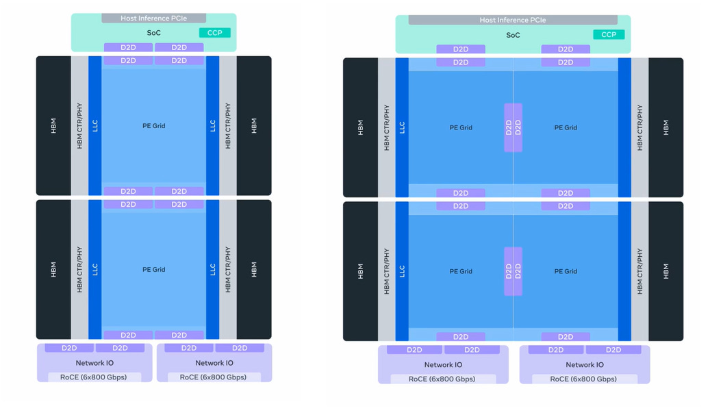
Meta MTIA 450 & 500
Meta: Four MTIA Chips in Two Years: Scaling AI Experiences for Billions
Industry data indicates that by 2026, non-GPU XPU accelerators will become the fastest-growing segment in data center compute investment, with a 22% annual growth rate, outpacing GPUs (19%) and CPUs (14%).
Impact on the DRAM and Packaging Industries
The LPU does not fully replace DRAM. Each LPX compute tray still integrates an x86 or ARM CPU along with DDR5 RDIMMs to support the operating system and control software. The BlueField-4 DPU is also equipped with 128 GB of LPDDR5 memory.
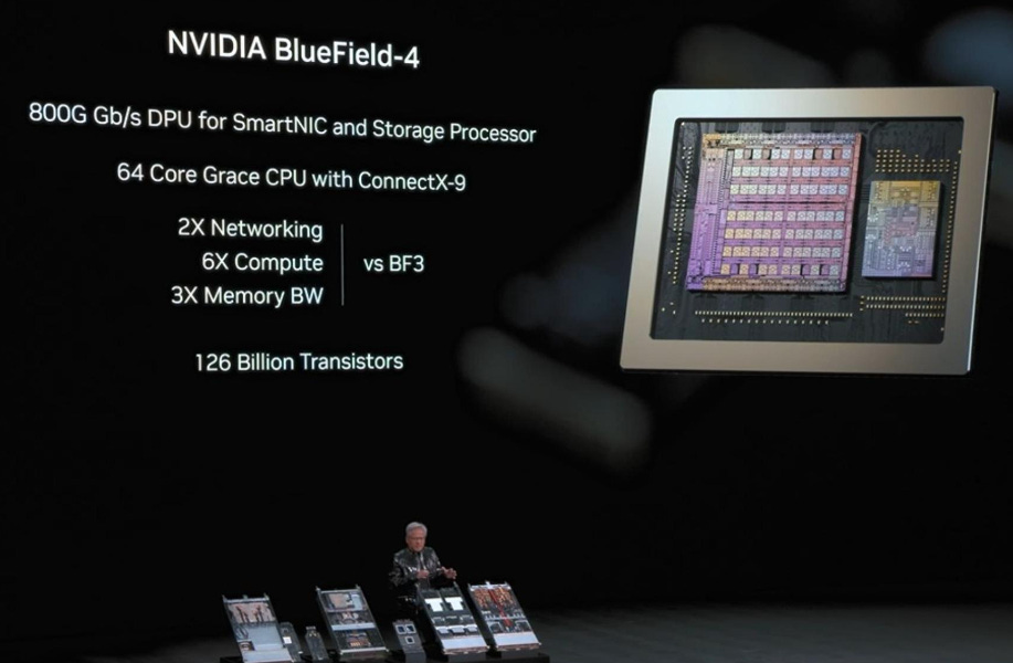
In fact, LPUs expand overall DRAM demand. A single LPX rack may be equipped with up to 12 TB of DDR5 DRAM.
Moreover, the LPX architecture allows SRAM-based workloads to operate without competing for HBM capacity. Samsung can manufacture LPU dies on its existing 4 nm process lines, while continuing to scale production on its HBM lines.
This creates a differentiated advantage for Samsung and provides an additional revenue stream beyond TSMC’s CoWoS-based packaging ecosystem.
Competitive Landscape and Strategy
The alliance between NVIDIA and Samsung places significant pressure on other inference accelerator companies.
SRAM-based startups such asCerebrasandd-Matrixoffer advantages in inference efficiency, but lack the extensive CUDA ecosystem and software stack support. By licensing Groq’s technology and integrating it into its own platform, NVIDIA leverages its existing CUDA and TensorRT toolchains to provide customers with a seamless compilation and deployment environment.
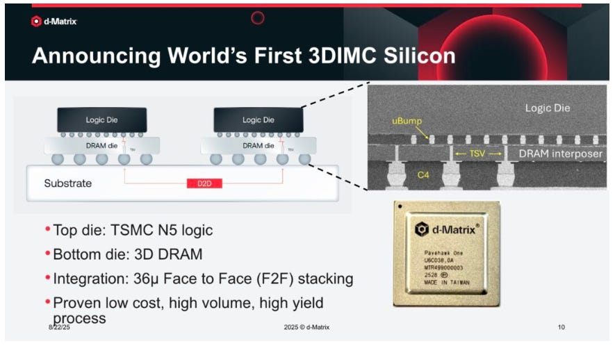
d-Matrix’s represents a new approach to AI inference by introducing3DIMC (3D Digital In-Memory Compute)—a technology that vertically integrates DRAM and compute logic to directly address the “memory wall” problem. Unlike traditional GPU architectures that rely on expensive and supply-constrained HBM, Pavehawk tightly couples memory and compute through 3D stacking, enabling higher bandwidth, lower latency, and improved energy efficiency.
Designed specifically for inference workloads, this architecture allows computation to occur closer to where data resides, significantly reducing data movement overhead. d-Matrix claims that 3DIMC can deliver up to 10× better performance and energy efficiency compared to HBM-based systems, positioning it as a potential alternative for scalable, cost-effective AI inference infrastructure.

Overall, d-Matrix reflects a broader industry shift: moving from compute-centric to memory-centric architectures as inference becomes the dominant workload in AI data centers.
Cerebras Systemsis an AI hardware company known for developing theWafer-Scale Engine (WSE)—the largest chip ever built, designed specifically for accelerating AI workloads.

Instead of using many smaller chips like GPUs, Cerebras integrates an entire wafer into a single processor, enabling massive on-chip memory, high bandwidth, and extremely fast data movement. This architecture is particularly effective for large-scale AI training and inference, where minimizing data transfer bottlenecks is critical.
Cerebras positions itself as an alternative to GPU-based systems, offering simplified scaling, high performance, and improved efficiency for frontier AI models.

2025 saw a wave of consolidation among inference chip companies, including AMD acquiring the Untether AI team, Meta acquiring Rivos, and Intel investing in SambaNova.
This trend suggests that independent inference startups are finding it increasingly difficult to compete within the dominant GPU ecosystem, pointing toward a likelyoligopolistic market structurein the future.
Deep Dive: SRAM Scaling and Performance Analysis
How to Integrate 512 MB of SRAM on an ASIC
Integrating 512 MB of SRAM on a single ASIC requires a massive silicon area. At the 4 nm node, an SRAM cell typically occupies around 0.02 μm² per bit, which is approximately 6–8× larger than a DRAM cell. Achieving this level of integration means dedicating a substantial portion of the die area to memory.
According to Gimlet Labs’ comparison of SRAM density across architectures:
NVIDIA B200 GPU (4 nm, dual-die): ~1600 mm² die area with126 MB L2 cache(~0.08 MB/mm²)
Groq LPU v1 (14 nm):230 MB SRAM(~0.32 MB/mm²)
d-Matrix Corsair (6 nm):256 MB SRAM(~0.64 MB/mm²)
Cerebras WSE-3 (5 nm):44 GB SRAM(~0.97 MB/mm²)
Cerebras achieves the highest density through its wafer-scale engine, while the LP30, built on 4 nm, integrates 512 MB of SRAM with a density of approximately 0.32 MB/mm², placing it between d-Matrix and Cerebras.
To achieve this density, the LPU adopts a multi-bank + tiled architecture. SRAM is partitioned into thousands of independent banks, distributed across the east and west sides of the chip. Compute tiles and memory tiles (MEM) are tightly coupled, separated only by short physical distances to minimize signal propagation delay.
The compiler maps working sets to specific banks to avoid runtime conflicts and schedules data movement at each cycle. This design allows aggregate bandwidth to scale nearly linearly with the number of banks. As noted by StorageReview, each LPU can deliver 2.5 TB/s of inter-chip bandwidth through 96 C2C links.
How Is 150 TB/s SRAM Bandwidth Achieved?
The internal SRAM bandwidth of a single LPU reaches 150 TB/s, which represents the aggregate bandwidth across all memory banks. If examining a single data path—for example, between compute units and MEM blocks—the bandwidth may be in the multi-terabyte-per-second range.
This level of bandwidth is enabled by several key architectural techniques:
Massive Port Count and Banked Architecture
Each SRAM bank supports multiple read/write ports, allowing multiple compute tiles to access different banks simultaneously. For example, with ~2000 banks, each 128 bits wide, operating at 1.5 GHz, the aggregate bandwidth can reach hundreds of TB/s. Since SRAM does not require refresh cycles, each bank can deliver data every clock cycle.
Pipelined Streaming Fabric
The LPU employs an east–weststreaming fabric, where data flows through pipelines at a fixed rate. Compute tiles synchronize with MEM at specific clock cycles to retrieve data, eliminating the need for global arbitration.
Compiler-Driven Scheduling
All data paths and timing are scheduled at compile time, avoiding bank conflicts. Dynamic scheduling would introduce latency and jitter, whereas the LPU’s compiler-controlled execution ensures predictable read/write timing and deterministic performance.
Power and Area Trade-offs of SRAM Architectures
Despite its low latency, SRAM comes with significantly higher area and power consumption compared to DRAM.
To mitigate static leakage, the LPU employs power gating and hierarchical clock gating, selectively shutting down unused memory banks during operation.
At the architectural level, designers must balance compute and memory resources. Allocating large amounts of SRAM inevitably reduces the number of arithmetic units. This is why each LPU delivers around 1.23 PFLOPS of compute performance, compared to tens of PFLOPS in a B200 GPU.
Rather than maximizing raw compute throughput, the LPU is explicitly optimized for memory bandwidth-bound workloads, where data movement—not arithmetic—is the dominant bottleneck.
GPU and LPU: Complementary Roles and Case Analysis
Agentic Inference Scenarios
In agent-based AI systems, each request often involves multiple rounds of inference, retrieval, and tool usage—such as calling external APIs, querying databases, or executing programs. The accumulated latency across these loops directly impacts user experience.
GPUs are designed for high throughput and can process large batches efficiently, but their optimization is primarily geared toward training and batch inference. When GPUs are used alone for serial decode, latency from shared memory and L2 cache hierarchies becomes amplified, leading to increased tail latency.
The LPU fills this gap. By leveraging 512 MB of on-chip SRAM, it stores model weight segments and intermediate activations locally, enabling near-zero-latency execution of FFN/MoE operations and significantly reducing token latency.
ServeTheHome emphasizes that the decode stage is more sensitive to memory latency than prefill. The LPU addresses this weakness of GPUs in sequential inference through its specialized architecture.
Performance Gains
When paired with an NVL72 GPU system, an LPX rack can deliver up to 35× higher inference efficiency, reducing compute cost to approximately $45 per million tokens.
Tom’s Hardware reports that a single LPU chip can generate thousands of tokens per second, bringing per-user latency down to the millisecond level.
These performance gains stem fromhardware co-design:
GPUs provide high-FLOPS parallelism for prefill and attention
LPUs deliver ultra-low-latency execution for FFN/MoE and draft generation
Both are seamlessly coordinated through Dynamo scheduling, ensuring deterministic data exchange within fixed clock cycles and eliminating unpredictable jitter.
Convergence of Market and Technology
3D Integration and NVLink Evolution
Although current LPUs are not tightly integrated with GPUs via NVLink, future generations (e.g., LP35 / LP40) may join the NVLink domain, enabling shared address space between LPUs and GPUs.

This would reduce the latency of transferring intermediate activations over Ethernet/RDMA and improve the efficiency of the AFD loop.
Meanwhile, research is exploring 3D SRAM stacking, such as multi-layer SRAM dies or eDRAM, to increase capacity without expanding 2D die area. If SRAM capacity can scale beyond 2 GB, LPUs may be able to host more model layers independently, reducing reliance on GPUs.
Software Stack and Ecosystem
The success of LPU depends not only on hardware, but also on the maturity of its software ecosystem.
Through tools such as CUDA, TensorRT, and Triton Inference Server, NVIDIA enables developers to compile PyTorch/TensorFlow models directly onto LPUs.
Dynamo acts as the orchestrator, partitioning the model graph and determining which operators run on GPUs and which on LPUs. This integration allows users to benefit from LPU acceleration without rewriting code, significantly lowering adoption barriers.
Future versions are expected to support additional data formats, such as FP4 / NVFP4, and integrate with higher-level frameworks like agentic AI pipelines (e.g., RTX-based systems).
Implications for Taiwan’s Semiconductor Industry
Taiwan remains a global semiconductor hub with strong capabilities in foundry and advanced packaging.
Reduced reliance on HBM in LPU-based architectures may slightly ease pressure on TSMC’s CoWoS capacity, but with Samsung manufacturing LPUs, TSMC faces new competitive dynamics.
Taiwan’s supply chain can still participate in the heterogeneous inference ecosystem by providing:
DDR5 / LPDDR5 modules
Server motherboards
Networking switches
Additionally, local companies can explore SRAM-first architectures and 3D SRAM stacking technologies, either through collaboration with global players or through independent development.
Future Outlook: Compatibility and Continuous Innovation
In the long term, the LPU is not a replacement for GPUs, but a complement.
Inference workloads are diverse, and some still require large memory capacity and high arithmetic intensity—areas where GPUs remain indispensable. The LPU fills the gap in low-latency, sequential inference and agentic AI workloads.
Over the next few years, several key trends are likely to emerge:
Diversification of inference accelerators
Beyond LPUs, architectures such as d-Matrix Corsair (SRAM-based), Cerebras WSE, and MoE-specific ASICs will compete across different model sizes, sparsity levels, and algorithmic needs.
Tighter heterogeneous integration (NVLink / NVSwitch)
Integrating LPUs into NVLink domains or leveraging NVSwitch will reduce GPU–LPU latency and support larger KV caches and more complex models.
Mainstream adoption of speculative decoding
With draft models running on LPUs, speculative decoding will become standard. Software stacks will need to dynamically orchestrate draft and verifier models and adjust token batching strategies.
Memory innovation
Emerging memory technologies such as eDRAM, MRAM, and PCM may offer intermediate trade-offs between SRAM and DRAM in the next 5 years, impacting LPU-like architectures by redefining the balance between speed, cost, and capacity.
Energy efficiency and sustainability
AI inference consumes significant power. LPUs, with high compute density and low latency, reduce total loop iterations and tail latency, improving system-level energy efficiency compared to GPU-only systems. Future gains will come from DVFS (dynamic voltage and frequency scaling) and material innovations such as GaN-based power systems.
Conclusion
Large language models and agentic AI demand high real-time responsiveness and stability. Traditional GPU architectures, optimized for throughput, face limitations in sequential decode workloads.
The NVIDIA Groq 3 LPU and LPX system, with 512 MB on-chip SRAM, 150 TB/s bandwidth, and a deterministic execution model, introduces a new direction for inference computing.
Through AFD disaggregation, GPUs handle prefill and attention at high throughput, while LPUs accelerate bandwidth-intensive FFN/MoE operations. This division significantly reduces latency without sacrificing throughput—improving both user experience and energy efficiency.
Samsung’s role highlights the strategic importance of process technology and memory supply. Its 4 nm high-yield process, combined with DDR5/LPDDR5 and BlueField DPUs, enables a robust heterogeneous inference platform.
At the market level, the rise of inference ASICs is reshaping the semiconductor industry—from a pure focus on compute scaling (Moore’s Law) toward memory bandwidth and latency optimization. Over the next 3–5 years, heterogeneous computing will become the norm, with diverse XPUs competing and collaborating within the AI infrastructure stack.
In summary, the SRAM-driven LPU architecture does not replace GPUs—it completes them. Through thoughtful system design, supply chain coordination, and software ecosystem integration, the GPU + LPU combination will deliver more efficient, cost-effective, and scalable solutions for next-generation AI inference.


PreviousNext
TopLatestDiscussions








See all