OFC 2026 Summary: How Silicon Photonics, CPO, OCI, and OCS Are Redefining the Physical Boundaries of Data Centers
OFC 2026 Summary: How Silicon Photonics, CPO, OCI, and OCS Are Redefining the Physical Boundaries of Data Centers
- Source: SemiVision
- Author: SEMIVISION
- Published: 2026-03-26T23:02:44+08:00
- URL: https://tspasemiconductor.substack.com/p/ofc-2026-summary-how-silicon-photonics (1) OFC 2026 Summary: How Silicon Photonics, CPO, OCI, and OCS Are Redefining the Physical Boundaries of Data Centers


OFC 2026 Summary: How Silicon Photonics, CPO, OCI, and OCS Are Redefining the Physical Boundaries of Data Centers
Original Article By SemiVision Research [Reading time: 25 mins]

Mar 26, 2026
∙ Paid
OFC 2026: The Moment AI Infrastructure Moved Beyond the Chip
If the dominant theme of the semiconductor industry over the past decade was process scaling, then what truly stood out at OFC 2026 was a deeper and far more structural shift:
In the AI era, the bottleneck is no longer just within the chip itself—
it lies between chips, between racks, and between switches and accelerators.
The real question is whether we can connect the entire system—
with acceptable power consumption, manageable latency, and manufacturable packaging.
This is the essence of OFC 2026.
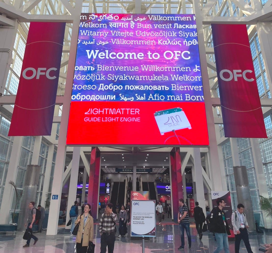
Optical communications is no longer just a showcase for modules, lasers, DSPs, or switching components. It has officially become a system-level battlefield for AI infrastructure.
From NVIDIA’s definition of the AI Factory, to Meta’s 90-million-hour reliability validation for CPO; from Broadcom pushing CPO toward commercial maturity, to Intel driving OCI into the package; from ST and Samsung bringing silicon photonics onto 300mm platforms, to FormFactor and GF/Cadence tackling testing and EDA—two of the least glamorous yet most critical barriers to scale—
the entire industry is, in fact, answering the same question:
As AI clusters scale to 100K, 500K, or even 1 million GPUs, what should the future data center interconnect actually look like?

3月17日
OFC 2026: Not a Telecom Show, but a Debate on “System Physics” in the AI Era
In this context, OFC 2026 was not merely an optical communications conference.
It was an open debate about the“system physics”of the AI era.
Because when:
Rack-level power scales from 120 kW to 600 kW,
A single AI factory demands hundreds of megawatts,
Both training and inference begin treating networking as a first-class resource, interconnect is no longer a supporting role—it becomes core infrastructure that determines whether compute can be monetized.
NVIDIA articulated this clearly at the conference:
“The data center is a computer, and the network defines its boundaries.”
What this really implies is:
The future competition is not just about who has more GPUs—
but who can assemble those GPUs into a working AI factory with:
The lowest pJ/bit,
The smallest failure domain (blast radius),
The highest serviceability.
The Real Bottleneck of AI Factories: Not Compute, but Whether Interconnect Can Keep Up with Agentic Scaling
Historically, discussions around AI infrastructure have focused on GPUs, HBM, advanced packaging, and process nodes, but at OFC 2026 one signal became unmistakably clear: the performance scaling of compute cores is now outpacing the scaling of I/O and networking, fundamentally shifting the bottleneck. The key question is no longer whether a single chip is fast enough, but whether the entire cluster can operate as if it were a single chip.
From Bandwidth to Architecture: Scale-Up vs. Scale-Out
This is why companies across the spectrum— OpenAI, Microsoft, AMD, NVIDIA, and Broadcom— are shifting the discussion:
From raw bandwidth → to architectural partitioning between scale-up and scale-out
Scale-up: ultra-low latency, high synchronization efficiency between accelerators
Scale-out: throughput, elasticity, and scalability across racks and clusters
In the past, both domains could partially rely on shared copper interconnects and electrical switching architectures.
But as model sizes and data flows explode, that assumption is breaking down.
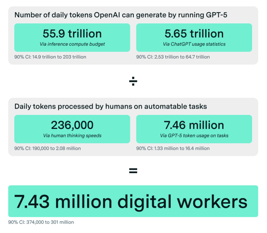
OpenAI’s framing at the conference was particularly direct: inference token growth is no longer linear but expanding by orders of magnitude, which implies that each new generation of infrastructure must simultaneously deliver roughly 2× improvements in bandwidth density while continuously reducing I/O power; otherwise, the economics of the AI factory will deteriorate rapidly.
Source: epoch.ai
Below we will share:
Silicon Photonics Has Finally Entered the True 300 mm Era—But the Bottleneck Is No Longer Just the Device
1.6T Is No Longer the Future — The Real Battlefield Lies in 3.2T and Beyond 400G/lane
From Pluggables to CPO to OCI: The Interconnect Boundary Keeps Moving Closer to the Chip
Meta Has Answered the Hardest Question Around CPO: Reliability
NVIDIA, Lightmatter, and Broadcom Represent Three Different Futures: High-Density Microrings, In-Package DWDM, and System-Level CPO
The Real Implication for Taiwan and the Supply Chain: The Center of Value in Optical Interconnects Is Shifting from Modules to Platforms and Packaging
The Real Theme of OFC 2026: How Deep Optical Integration Goes Inside the Data Center
This leads to the real theme of OFC 2026: it is not about which optical module is better, but about how deeply optical interconnect can penetrate into the data center architecture. Historically, optics operated at the periphery—rack-to-rack, row-to-row, and across data center interconnects (DCI). Today, that boundary is rapidly moving inward: into the rack, onto the board, toward the package edge, and even approaching the chip perimeter. Each step inward is not merely a product evolution, but a fundamental rewrite of system architecture.
From:
→ Pluggable optics
→ Linear pluggable optics (LPO)
→ Near-packaged optics (NPO)
→ Co-packaged optics (CPO)
→ Optical I/O (OIO)
This is not merely a form factor transition.
It is a transformation from:
“Electric-dominant, optics-assisted” architecturesto
“Electro-optical co-design—and in some domains, optics-first systems.”

Source: ASE
Silicon Photonics Has Finally Entered the True 300 mm Era—But the Bottleneck Is No Longer Just the Device
If one sentence were to summarize the significance of OFC 2026 for silicon photonics manufacturing, it would be this: silicon photonics has finally moved from “can be built” to “can be mass-produced,” but the real point of competition is no longer at the level of individual devices—it lies in whether the entire ecosystem of platforms, testing, PDKs, packaging, and design tools can mature in sync.
Two of the most representative examples areSTMicroelectronics’ PIC100 platform andSamsungFoundry’s 300 mm silicon photonics platform.

The importance of ST’s PIC100 platform is not just that it supports 200G per lane, but that it demonstrates the transition of silicon photonics from discrete components to a system-level platform. Built on 300 mm wafers, it integrates front-end SOI waveguides, Ge photodetectors, modulators, and TiN heaters, while also incorporating backside integration to bring in 400 nm SiN waveguides and edge couplers, forming a structure with 5 µm optical isolation. What this really addresses is a critical issue: future high-speed silicon photonics platforms cannot simply optimize individual components—they must achieve a system-level balance across thermal behavior, loss, coupling, and packaging compatibility. The performance metrics of PIC100—such as 80 GHz Ge photodetectors, 1 A/W responsivity, 11 nA dark current, 0.6 dB/cm silicon waveguide loss, and 0.5–0.6 dB edge coupler loss—make it clear that ST is not building a showcase, but rather a platform designed to transition toward NPO and CPO architectures.
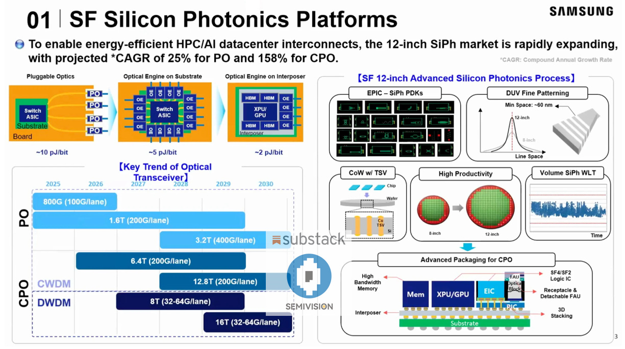
Samsung’s approach carries a different implication. Rather than presenting a single platform to demonstrate capability, Samsung is signaling through its full IDM + foundry model that silicon photonics will not exist as a standalone photonics process—it must be co-developed alongside HBM, XPU, advanced packaging, and the broader 300 mm manufacturing ecosystem.
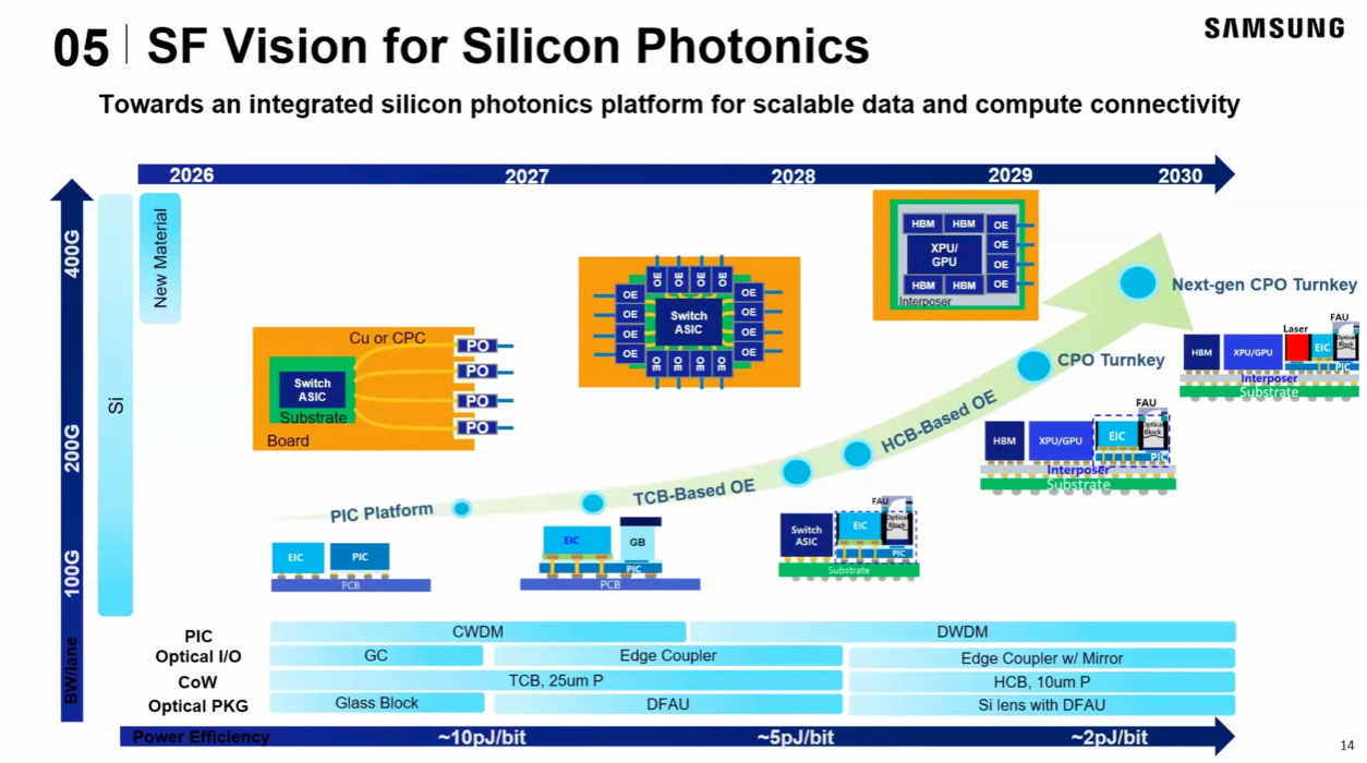
At OFC 2026, Samsung showcased key metrics including 1.4 dB/cm Si strip loss, 0.7 dB/cm Si rib loss, and 0.4 dB/cm SiN loss, alongside inverse-designed 2D grating couplers, MZMs exceeding 50 GHz, microring modulators with 55 pm/V efficiency, and Ge photodetectors reaching 100 GHz. While these figures are important, what matters more is the roadmap behind them: a transition from pluggable optics at around 10 pJ/bit toward CPO-level efficiency of ~2 pJ/bit by 2030. This reflects Samsung’s strategy of presenting not just isolated demonstrations, but a full pathway to integrating silicon photonics into mainstream advanced manufacturing and packaging.
If ST and Samsung represent progress on the manufacturing platform side, then GlobalFoundries and Cadence represent a fundamental catch-up on the design tool side. Historically, one of the key challenges in photonic circuit design has been that many models attempt to describe optical behavior using frameworks originally built for electronic design, limiting both efficiency and accuracy when simulating large-scale, multi-wavelength, multimodal, and bidirectional systems.
The photonic-native compact modeling introduced by GF and Cadence essentially argues that if silicon photonics is to become a true large-scale IC platform—rather than a collection of stitched-together components—EDA must be built on native optical physics. Their models support simultaneous forward and backward wave modeling, deliver up to 2× simulation speed improvements at system scales with tens of thousands of components, and enable system-level verification of over 80 validated hardware components, including WDM thermal coupling and reflection effects. These are not incremental features, but necessary conditions for achieving true high-volume manufacturing.
Perhaps most importantly, by OFC 2026 the hardest challenge in scaling silicon photonics has clearly shifted. The bottleneck is no longer primarily in front-end process technology—it is now in testing.

FormFactor’s Pharos is one of the clearest demonstrations of this overarching trend. Historically, PIC testing has been expensive due to its heavy reliance on optical alignment, mechanical precision, and inherently low-throughput processes. Pharos addresses this by automating the workflow through a combination of two-photon polymerization (2PP) 3D-printed micro-lenses, periscope-style edge coupling, collimated beams via grating couplers, and 3D beam scanning. The performance metrics are critical: edge coupling loss is reduced to 0.5 dB per facet, measurement stability improves by 10×, angular repeatability is kept below 0.13°, and the Skip Die Strategy boosts throughput by 1.8–2.5×.
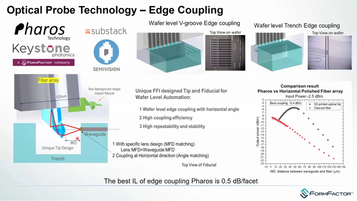
This points to a fundamental shift: the future competition in silicon photonics will not be defined solely by faster modulators, but by who can industrialize the entire chain—from yield discovery and validation to packaging yield—into a semiconductor-like manufacturing process.
In other words, the biggest breakthrough for silicon photonics at OFC 2026 is not just higher speed, but the industry’s transition from “building components” to “establishing scalable manufacturing methodologies.”
1.6T Is No Longer the Future — The Real Battlefield Lies in 3.2T and Beyond 400G/lane
If OFC 2024–2025 was still about when 1.6T would become commercially viable, by OFC 2026, 1.6T has effectively become the baseline assumption. What now differentiates industry trajectories is how to approach 3.2T and 400G per lane.

3月4日
At its core, this is not simply a matter of scaling each lane from 200G to 400G. The entire interconnect system has entered a new engineering regime—one where electrical–optical interfaces, modulator bandwidth, DSP complexity, laser power, packaging thermal density, and testing difficulty all rise simultaneously. As a result, the various approaches presented at OFC 2026 are not just technical options—they represent fundamentally different worldviews.
OpenLightstands out as a leading proponent of heterogeneous integration. Its 1.6T DR8 PIC does more than integrate DFB lasers, EAMs, SOAs, and photodetectors—it further co-packages a 400G/lane III-V-on-silicon EAM with a MACOM driver. The reported metrics are telling: 3 dBm OMA, extinction ratio exceeding 3.5 dB, and power consumption on the 1.6T DR8 evaluation board reduced from 2.7 W in early samples to around 2.0 W.

Openlight carrys a clear message: if future 3.2T systems and 400G/lane architectures are to balance bandwidth, power efficiency, and packaging integration, heterogeneous integration is not just viable—it may be the most practical path to high-volume manufacturing.
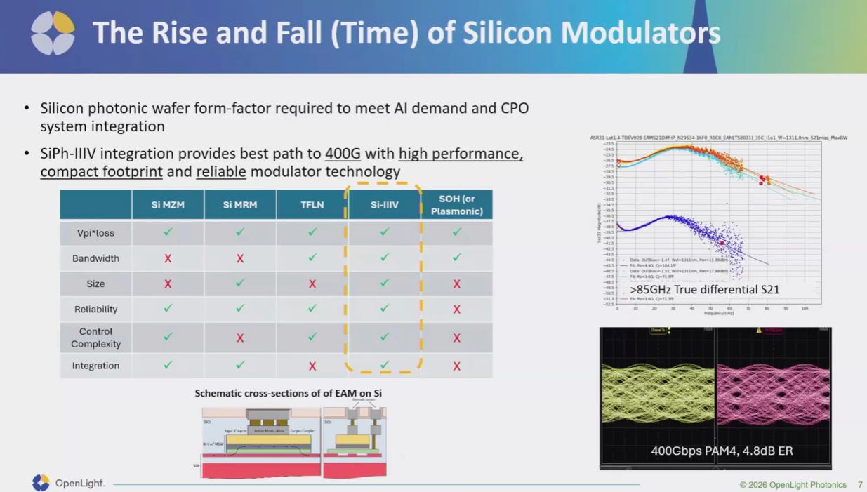
Equally notable is that OpenLight is no longer presenting just components. By showcasing alongside GDS Factory, Spark Photonics, and Oriole Networks, it is actively building a design and system ecosystem—signaling a strategic shift toward becoming a platform company.
Coherent, by contrast, represents a multi-platform parallel strategy. Rather than betting everything on a single technology path, it showcased a broad portfolio at OFC 2026, including 1.6T SiPh PICs, InP CW lasers, InP EMLs, and GaAs VCSEL solutions. Moving toward 3.2T, it further demonstrated 400G differential EMLs alongside pure-silicon PN junction Mach–Zehnder modulators.
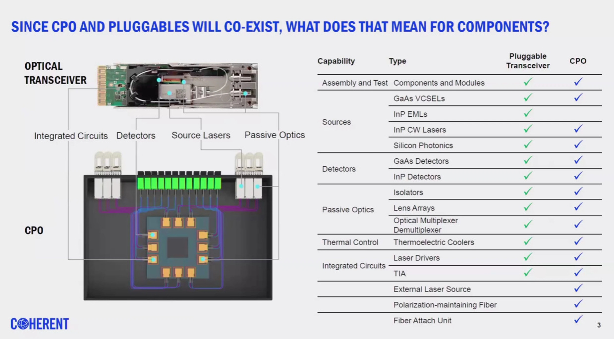
The logic behind this approach is clear: the dominant solution for 400G per lane is unlikely to converge into a single path anytime soon. Some applications will favor the maturity and performance of InP/EML, others will lean toward the scalability of pure silicon platforms, while short-reach, high-density use cases may revert to VCSEL-based solutions. Coherent even previewed a multi-lane XPO pluggable MSA targeting beyond 12.8T, signaling that it does not view 3.2T as an endpoint, but rather as a transitional step toward higher-generation systems.
Lumentum, on the other hand, positions itself more as a light source and system enabler. Its key signal at OFC 2026 was not just the 1.6T DR4 OSFP module, but its demonstration of ultra-high-power lasers and 16-channel DWDM ELSFP solutions. The 1310 nm single-mode high-power (SHP) laser delivers over 1 W of optical power at 25°C and remains above 800 mW at 50°C, with linewidth below 100 kHz and SMSR exceeding 40 dB. Meanwhile, its 16-channel DWDM light source uses two ELSFP modules to generate 16 wavelengths on a 200 GHz grid, each channel reaching approximately 24 dBm.
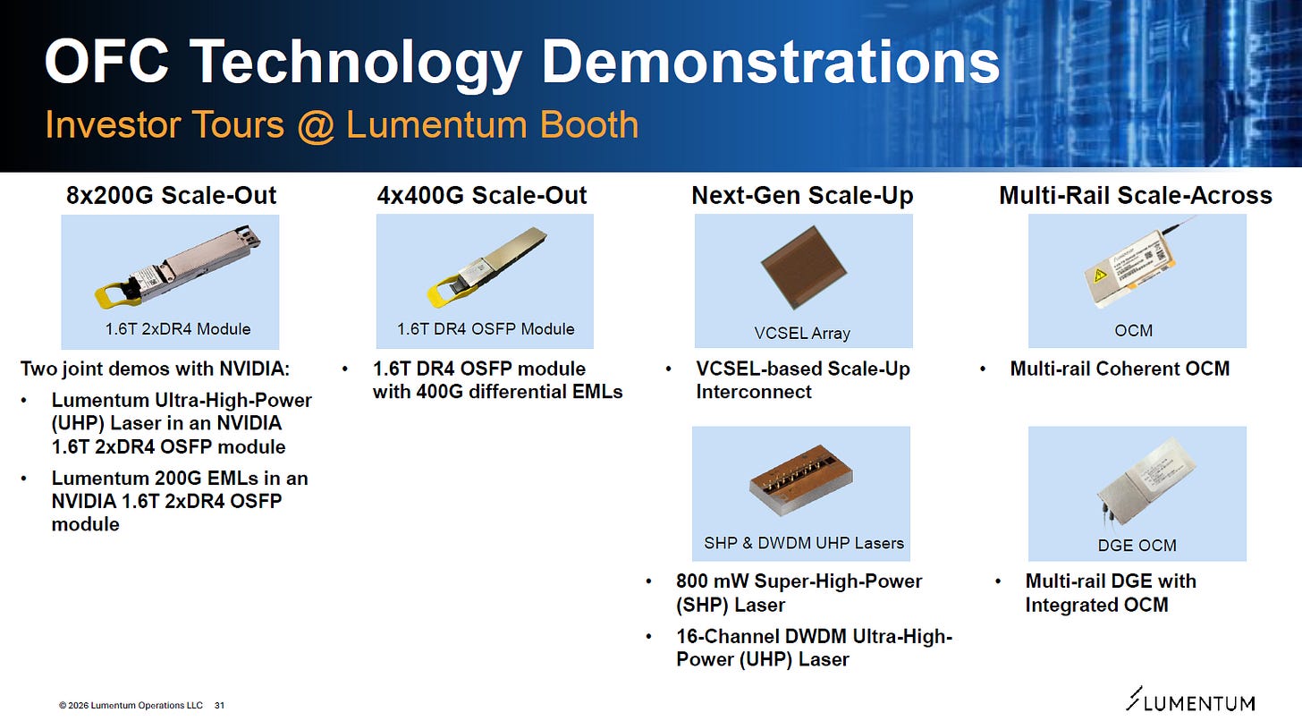
These metrics send a clear message to the market: as interconnect architectures evolve toward CPO, OCI, and high-density DWDM, the real bottleneck may no longer be the optical module itself, but rather the performance and management of external lasers and light sources.
From Pluggables to CPO to OCI: The Interconnect Boundary Keeps Moving Closer to the Chip
The rapid adoption of optical modules in the past was driven by a simple value proposition: they were replaceable, serviceable, and supported by a mature supply chain. But by OFC 2026, it has become clear that these advantages alone are no longer sufficient. As bandwidth density continues to rise and power consumption becomes a first-order cost in AI factories, optics must move closer to the chip to meaningfully reduce total system energy.

Broadcomprovided one of the most direct comparisons: at 100G per lane, DSP-based pluggables consume around 15 pJ/bit, LPO reduces that to roughly 10 pJ/bit, while CPO can bring it down to about 6 pJ/bit. This is not a marginal improvement—it is a system-level power step-change. In an AI data center with millions of optical interconnect points, such differences scale directly into megawatt-level power savings. Broadcom’s strong presence at the event was not just based on theory, but on real data: its TH5-Bailly 51.2T switch, validated with Meta, demonstrated the first 1 million hours without link flaps and an accumulated 50 million hours without unrecoverable failures. This marks a turning point where CPO moves beyond being “technically elegant” to becoming genuinely compelling under hyperscaler procurement criteria.
However, this does not mean pluggables or LPO are being displaced. In fact, perspectives from Microsoft, Oracle, and Arista make it clear that the market will not converge on a single architecture anytime soon. Microsoft is focused on scale-up system requirements—distances beyond 20 meters, bandwidth exceeding 50 Tbps, round-trip latency under 1 microsecond, and energy efficiency below 4 pJ/bit. Oracle emphasizes blast radius and serviceability in large-scale clusters. Arista, more bluntly, criticizes fully soldered architectures as too rigid, advocating instead for socketed or open CPO designs, where optical engines can be replaced much like CPUs.
In other words, CPO wins on power efficiency but still carries inherent drawbacks in maintainability. Pluggables and LPO, while less efficient, remain far more practical from a supply chain and operational perspective.
This is precisely why NPO and XPO drew significant attention at OFC 2026.
Arista’s 12.8T XPO concept, for example, essentially consolidates the equivalent functionality of eight OSFP modules into a single liquid-cooled unit.

It is not a final solution, but a pragmatic transitional architecture. These approaches aim to strike a balance between CPO and pluggables—bringing optics closer to the ASIC to reduce loss and routing complexity, while preserving a degree of modular serviceability. Such hybrid architectures are likely to serve as critical stepping stones over the next two to three years.

Taking it one step further leads toOCI (Optical Compute Interconnect). The significance of this concept lies in the fact that it no longer treats optics as an external attachment at the switch or module level, but instead integrates optical I/O directly into the compute system itself. Intel is currently the most prominent advocate of this direction. Its proposed OCI chipset delivers end-to-end energy efficiency of around 5 pJ/bit, shoreline bandwidth density of 1 Tbps/mm, transmission distances exceeding 10 meters, and added latency below 10 ns. It also leverages UCIe to enable “wide and slow” die-to-die connections, reducing traditional SerDes power consumption by 3–4 pJ/bit. The key to this strategy is not only light source integration—such as InP on silicon with over 40 million units shipped and FIT rates below 0.1—but also a fundamental redefinition of system boundaries: shifting high-speed data transmission challenges from the PCB level into the package and chiplet interface.
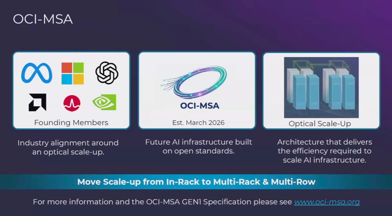
From a broader perspective, this evolution—from pluggables to LPO/XPO/NPO, to CPO, and ultimately to OCI—represents a continuous migration of the optical boundary toward the compute boundary. With each step closer, power consumption decreases and density increases, but at the same time, challenges in serviceability, yield pressure, packaging complexity, and supply chain control all intensify. This implies that future winners will not simply be those with the best modulators, but those capable of integrating optics, electronics, packaging, thermal management, testing, and operations into a unified system.
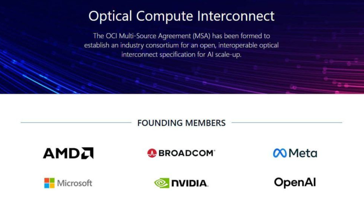
These three standards each address different layers of optical communication in AI data centers, providing a unified framework across the ecosystem:
OCI MSA:Defines the optical signaling formats and transmission protocols for scale-up interconnects—ultra-short-distance links within the rack, particularly between GPUs. It enables all devices to communicate using a common language, replacing copper-based solutions that are approaching their physical limits.
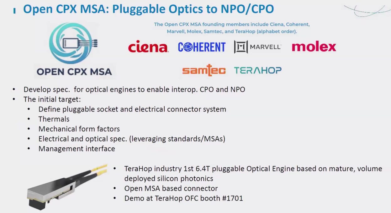
Open CPX MSA:Defines the socket and interface standards for optical engines mounted directly adjacent to chips. It enables interoperability across vendors for embedded optics such as NPO and CPO, addressing the long-standing issue of incompatible proprietary implementations.
Source: Terahop
XPO MSA:Specifies the form factor, thermal design, and mechanical requirements for external high-density optical modules. It is designed for scale-out connections between racks, significantly increasing front-panel density and thermal capacity, allowing a single module to handle much higher bandwidth.
Together, these three standards mark a transition for the industry—from a fragmented phase of vendor-specific approaches and incompatible specifications to a more standardized ecosystem capable of scaling into high-volume deployment.
Meta Has Answered the Hardest Question Around CPO: Reliability
The strongest argument against CPO has never been that it lacks power efficiency—it has been, quite simply, “What happens when it fails?” This concern is even more practical than power consumption, because in the hyperscaler world, the real risk is not that a module is expensive, but that it becomes a systemic maintenance nightmare at scale.
What makes Meta’s presence at OFC 2026 so significant is that, for the first time, it brought this debate into the realm of empirical data. Its presentation, based on 90 million cumulative device hours, showed that—excluding known and correctable issues related to PLS and laser drivers—CPO Phase 1 achieved an MTBF of 8.2 million hours. By comparison, a reference setup using 2×400G FR4 pluggables under 40°C stress conditions achieved only about 0.71 million hours. This is not a marginal improvement—it represents more than a 10× increase in reliability.

Source: meta
Meta also made a crucial clarification: the primary sources of failure were not inherent to the CPO architecture itself, but rather linked to degradation of SMT components in external laser driver circuits. In effect, this reframes the problem. Instead of being seen as an “architecturally flawed” approach, CPO is now understood as a viable architecture that still requires optimization at the implementation level.
This shift is critical because it fundamentally changes how the market talks about CPO.
The old narrative was: “CPO is efficient, but unreliable.” Meta’s updated narrative is: “CPO is not only efficient, but under certain conditions can be more reliable than pluggables—provided system design, external laser architecture, and service models are rethought.
”This is why discussions at OFC 2026 extended beyond CPO itself to include blind-mate optical backplanes, ELSFP, serviceability models, connector cleanliness, and upstream testing at the OSAT level. Once CPO is proven viable, the industry’s next challenge becomes how to redesign maintenance workflows and allocate manufacturing responsibility.
From a supply chain perspective, this has two major implications.
First,the importance of external laser suppliers increases significantly. As lasers become decoupled from optical engines, companies such as Lumentum, Broadcom, and Coherent—capable of delivering high-power, high-reliability external laser sources—become integral to overall system stability rather than just component vendors.
Second,testing shifts upstream into earlier stages of packaging. Future CPO systems will require not just module-level validation, but system-level optoelectronic testing at the packaging stage, elevating the strategic importance of OSATs, advanced packaging providers, and ODMs. This is why companies like TSMC, ASE, and Amkor are transitioning from backend enablers to structurally critical nodes in the optical interconnect ecosystem.
NVIDIA, Lightmatter, and Broadcom Represent Three Different Futures: High-Density Microrings, In-Package DWDM, and System-Level CPO
If one were to distill the many technical demonstrations at OFC 2026 into the most representative future directions, NVIDIA, Lightmatter, and Broadcom would stand out—each representing a different layer of the answer.
Lightmatter’s significance lies in proving that microring modulators are no longer just a high-density academic concept, but a viable foundation for commercial AI interconnects. Its demonstrated 16-wavelength, 800 Gbps bidirectional single-mode fiber link—based on 50 Gbps NRZ, achieving 1E-9 BER without FEC, 2.6 pJ/bit energy efficiency, and transmission distances up to 1 km—comes remarkably close to real-world deployment requirements.

More importantly, its experiments showed stable BER across 25–105°C thermal cycling, corresponding to the ability to track temperature variations on the order of 2000°C/s. This directly addresses the long-standing concern around microrings: whether thermal stability can withstand the dynamic workload fluctuations of AI accelerators. If the answer is yes, microrings are no longer just a density advantage—they become a leading candidate for short-reach, high-density optical interconnects.

1月29日
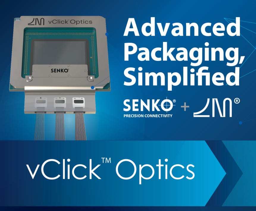
AI infrastructure demands more bandwidth and tighter integration.Lightmattermeets the challenge with vClick™ Optics, a next-generation 3D photonic interconnect architecture featuring SENKO Precision Connectivity for detachable fiber connectivity.
By integrating SENKO’s Metallic PIC Coupler (MPC) and SEAT™ optical interface, the solution delivers:
Detachable Fiber Array Units (FAUs) for advanced packaging environments
Serviceable optical interfaces for 3D photonic interconnects
<1.5 dB re-insertion loss for high-performance field serviceability
Scalable optical connectivity supporting 32–100 Tbps+ bandwidth
This breakthrough enables known-good optical engines prior to final integration, helping improve manufacturing yield while supporting the massive bandwidth requirements of AI infrastructure.
NVIDIA, by contrast, is advancing a more system-level philosophy. Its 256 Gb/s DWDM optical I/O is not about maximizing per-lane speed, but about redefining interconnect architecture closer to a future compute fabric. By leveraging TSMC’s COUPE and SoIC technologies, NVIDIA hybrid-bonds a 7nm EIC with a 65nm PIC in a face-to-face configuration, using clock forwarding and band-pass filtering to achieve an overall efficiency of 2.6 pJ/bit, a 6× improvement in shoreline density, and an area bandwidth density of 1.33 Tb/s/mm².

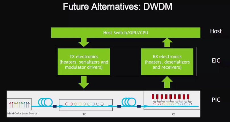
Source: NVIDIA
The core message is clear: the value of future interconnects lies not in pushing single-channel speed to the limit, but in packing more connectivity into the package boundary at lower power and area cost. This aligns directly with the logic of the AI Factory—when system-level power and cooling are constrained, performance per watt per mm² matters more than peak speed.
3月17日

3月18日
Broadcomrepresents the path of commercial maturity. It may not offer the most visionary narrative, but it understands hyperscaler priorities better than most: reliability, manufacturability, deployability, and total cost of ownership. By connecting its TH5-Bailly platform with the OCI MSA ecosystem, Broadcom effectively bridges two worlds—using CPO to reduce power in scale-out architectures, while leveraging 53G NRZ, 4-wavelength WDM, and Bi-Di technologies to compete with copper in scale-up scenarios. This reflects a distinctly Broadcom approach: not chasing the absolute limits of physics, but delivering sufficiently optimized industrial solutions to capture market share early. Its importance lies not only in execution, but in its ability to pull the entire supply chain toward lighter-weight, more linear, and lower-DSP optical architectures.

Together, these three paths point to a clear conclusion: over the next three to five years, optical interconnects will not converge into a single solution. However, all paths will move in the same direction—optics closer to the compute core, lighter DSP requirements, heavier reliance on advanced packaging, earlier-stage testing integration, and increasingly critical serviceability architectures.

2025年6月4日
Marvellpresented a comprehensive vision for its Photonic Fabric and silicon photonics CPO roadmap, targeting the scale-up network layer where traditional copper interconnects face fundamental reach limitations below two meters. By pushing beyond these physical constraints, Marvell aims to enable higher bandwidth density and improved energy efficiency within AI data centers. At the core of this strategy is its COUPE CPO technology, which leverages TSMC’s advanced N3P process and integrates electronic ICs (EIC) with photonic ICs (PIC) through hybrid bonding. This tightly coupled architecture significantly reduces signal loss and power consumption while improving latency.

The platform supports dense DWDM transmission with up to 16 wavelengths per fiber, achieving bandwidths of 1 Tbps per fiber. Combined with vertical integration features such as TSVs, silicon lenses, and co-packaged optics, Marvell is positioning itself to redefine short-reach interconnects and enable scalable, high-performance AI infrastructure.
OCS Is No Longer Just a Switching Technology—It Signals a Shift from Packet Logic to Optical Path Logic in AI Networks
If CPO and OCI address connection density and energy per bit, then OCS tackles a larger system-level question: when AI cluster traffic is no longer random, as in traditional cloud workloads, but instead consists of massive, predictable, repetitive, and synchronized data flows, do we still need every bit of data to pass through power-hungry electronic packet switching?
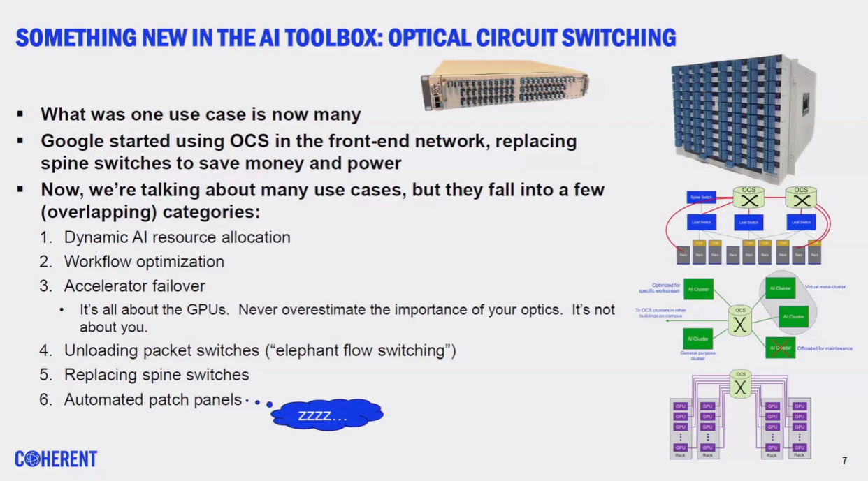
This is precisely why OCS moved from a peripheral topic to a central theme at OFC 2026. The official agenda explicitly highlighted Optical Networking for AI Datacenters, Photonic Switching for AI Infrastructure, and Scale-Out/Scale-Up Photonic Interconnects, effectively acknowledging a fundamental shift: the next generation of AI infrastructure will not be defined solely by faster NICs or switches, but by whether the network architecture itself can be rethought.

NTTpresents a vision of fully optical networking, emphasizing how IOWN/APN can push the optical layer all the way to the server, targeting end-to-end transmission energy at the pJ/bit level. NVIDIA takes a more pragmatic approach, viewing OCS not as a replacement for packet switching, but as a topology enhancer and fault-tolerance mechanism—used for reconfiguration and rerouting within Dragonfly or Fat-Tree architectures. Ciena focuses on high-radix OCS to minimize optical-electrical conversions, while Lumentum leverages its strengths in MEMS and LCoS components. Meanwhile, nEye Systems pushes switching latency below 500 ns, reflecting a more aggressive vision for photonic switching, and iPronics explores FPGA-like, software-defined photonic routing.

Despite these divergent approaches, the underlying convergence is clear:
OCS is driving data center networks from packet-based logic toward path-based logic.
As long as AI workloads exhibit large-scale, stable, and predictable communication patterns, optical circuit switching has the potential to outperform electronic packet switching in efficiency. For future AI factories operating at the scale of hundreds of thousands or even millions of GPUs, this efficiency is not just about saving power—it directly impacts training utilization, latency, and overall return on infrastructure investment.

3月19日
The Real Implication for Taiwan and the Supply Chain: The Center of Value in Optical Interconnects Is Shifting from Modules to Platforms and Packaging
From a SemiVision perspective, the most important takeaway from OFC 2026 is not any single laser or microring performance metric, but a structural shift in where value is being created across the supply chain.
The first shift is from modules to platforms. In the past, transceiver vendors were at the center of optical communications, but going forward, those who define optical I/O architectures, control PDKs, and own OSAT testing and packaging methodologies will move closer to the core of the value chain. This explains why companies like ST, Samsung, Intel, TSMC, and GlobalFoundries—historically not the primary players in optical modules—have become unusually prominent at OFC 2026.
The second shift is from board-level design to package-level design. Whether it is COUPE, SoIC, EMIB, hybrid bonding, or innovations like blind-mate backplanes and socketed optics, they all point to the same conclusion: future data center interconnect competition will no longer be defined at the PCB level, but will increasingly converge toward the package boundary. This creates strategic opportunities for TSMC, ASE, Amkor, SPIL, as well as materials and substrate suppliers.


2025年6月18日
The third shift is from component performance to system-level serviceability. Meta’s data has already demonstrated that the success of CPO will not be determined solely by pJ/bit, but by factors such as blast radius, connector cleanliness, ELSFP stability, upstream packaging-stage testing, and field serviceability models. The companies that ultimately win hyperscaler contracts will not be those that simply deliver faster components, but those that can make the entire deployment chain work seamlessly.
This is perhaps the most important implication for Taiwan. Taiwan’s strength in the AI era has never been a single technology node, but its ability to integrate foundry, packaging, substrates, testing, and ODM/EMS into a scalable manufacturing ecosystem. As the center of gravity in optical interconnect shifts from components toward packaging and platforms, this becomes precisely the domain where Taiwan holds the greatest strategic advantage. The question is not whether Taiwan can participate, but who will be the first to integrate SoIC, CoWoS, COUPE, optical engines, testing, thermal design, and serviceability into a complete, deployable solution.
3月24日
Conclusion: OFC 2026 Is Not a Routine Optical Conference—It Is the Inflection Point Where AI Infrastructure Begins to Rewrite the Rules of the Physical Layer
In summary, the most important signal from OFC 2026 is not which company demonstrated a faster module, but that the industry has collectively acknowledged a fundamental shift: the next bottleneck in AI infrastructure has moved beyond compute chips themselves, toward interconnects, packaging, light sources, topology, and serviceability.
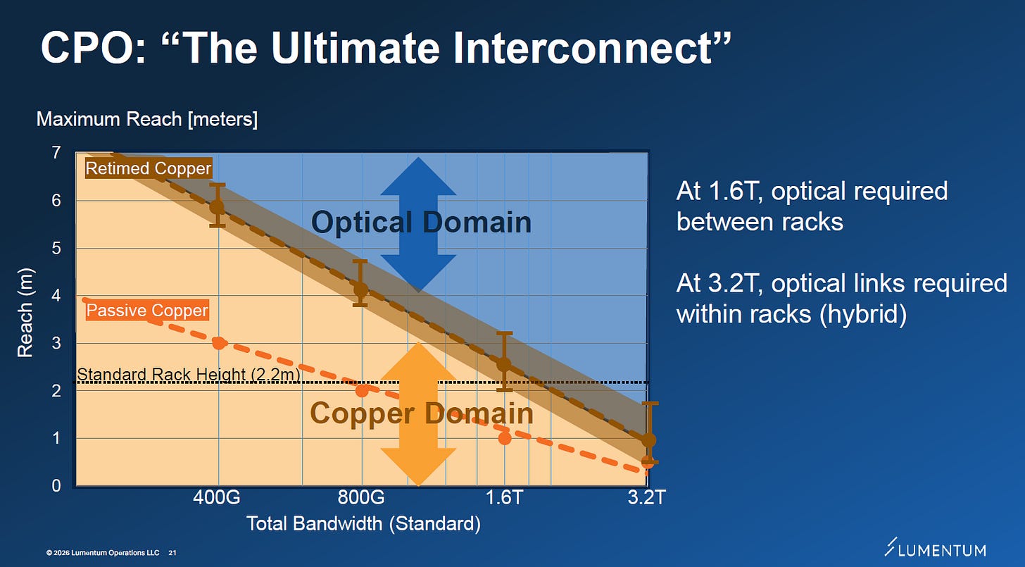
Silicon photonics entering the 300 mm era signals that it is now ready for mainstream high-volume manufacturing. Progress from FormFactor and GF/Cadence indicates that the final barriers—testing and EDA—are beginning to be resolved. OpenLight, Coherent, and Lumentum show that the competition around 1.6T, 3.2T, and 400G/lane is evolving along multiple parallel paths. Broadcom, Meta, Intel, and NVIDIA each offer distinct but complementary answers—from commercial maturity and reliability to in-package optical I/O and system architecture. Meanwhile, OCS points toward an even larger shift: the next-generation AI factory network may not simply be “faster switching,” but something closer to a reconfigurable optical fabric.
From a SemiVision perspective, the most important takeaway from OFC 2026 is not a specific technical slogan, but a simple and somewhat harsh reality:
As AI factories scale toward millions of GPUs, whoever can bring optics into the core of the data center—with the lowest power consumption, highest reliability, most advanced packaging, and most serviceable system design—will define the power structure of next-generation compute infrastructure.
This also implies that future competition will not be determined at the level of individual chips, but at the level of system boundaries. It is no longer about who can shrink transistors further, but about who can integrate light, packaging, networking, cooling, and software orchestration into a truly functional AI factory.

3月16日

OFC 2026
Thanks for reading SEMIVISION @_@! This post is public so feel free to share it.


PreviousNext
TopLatestDiscussions








See all