Silicon Photonics Industry Reshaping: The Netherlands as an Innovation Engine and Taiwan’s New Strategic Positioning
本頁目錄
Silicon Photonics Industry Reshaping: The Netherlands as an Innovation Engine and Taiwan’s New Strategic Positioning
- Source: SemiVision
- Author: SEMIVISION
- Published: 2026-03-24T09:24:33+08:00
- URL: https://tspasemiconductor.substack.com/p/silicon-photonics-industry-reshaping (1) Silicon Photonics Industry Reshaping: The Netherlands as an Innovation Engine and Taiwan’s New Strategic Positioning


Silicon Photonics Industry Reshaping: The Netherlands as an Innovation Engine and Taiwan’s New Strategic Positioning
Original Article By SemiVision Reserach [Reading time: 10 mins]

Mar 24, 2026
∙ Paid
Taipei, March 23, 2026 — The 2026 NL–TW TechBridge Program: Joint R&D Projects on Photonics Integrated Circuits, held alongside the Photonics Industry Exchange Forum, officially opened today in a well-attended launch event, bringing together representatives from government, industry, research institutions, and international partners to mark a new chapter in Taiwan–Netherlands collaboration on integrated photonics and advanced semiconductor-related innovation.
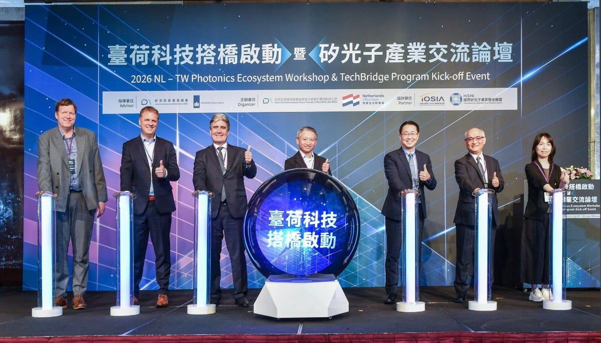
Source: Netherlands Office Taipei
The event, titled“2026 NL–TW Photonics Ecosystem Workshop & TechBridge Program Kick-off Event,”highlighted the growing strategic importance of photonics, semiconductor technologies, and cross-border innovation ecosystems. Distinguished guests and industry leaders gathered to witness the formal launch ceremony, underscoring the strong momentum behind bilateral cooperation between Taiwan and the Netherlands.
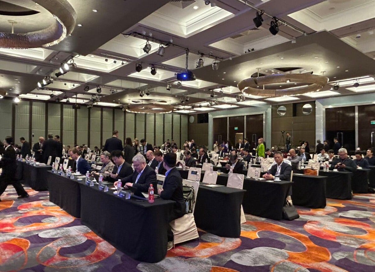
Source: Netherlands Office Taipei
At the center of this year’s program is the NL–TW TechBridge Program, a bilateral, market-driven industrial R&D and innovation initiative focused on photonics integrated circuits (PICs). According to presentations delivered during the event, the program represents the first bilateral market-driven industrial R&D and innovation program of its kind between the two sides in this field.
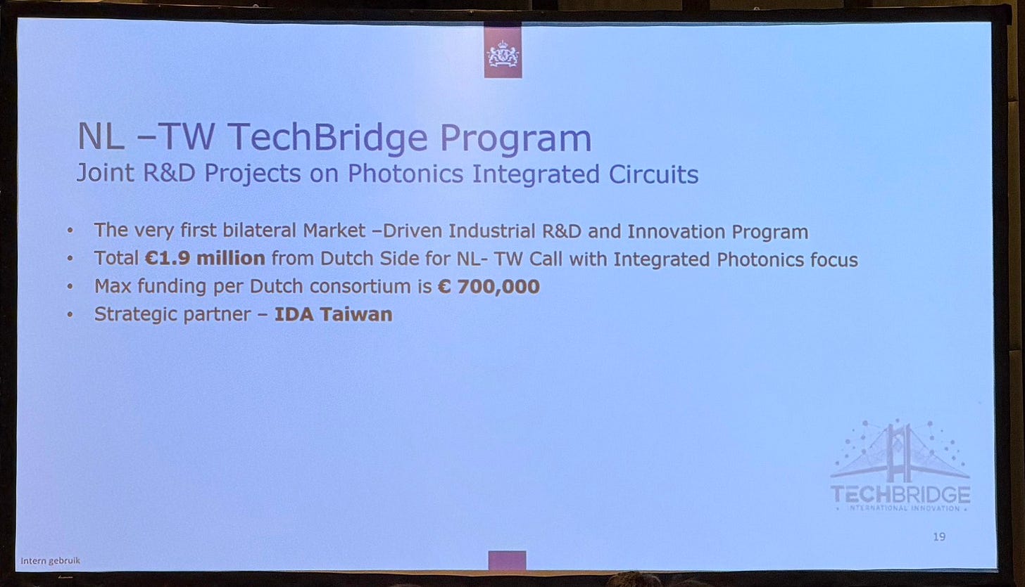
The Dutch side has allocated €1.9 million for the NL–TW call with an integrated photonics focus, with maximum funding of €700,000 per Dutch consortium, reflecting serious long-term commitment to joint innovation.


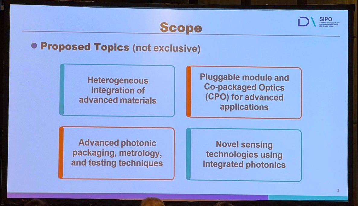
IDA emphasized that the TechBridge Program is designed not only to support individual projects, but also to build a multi-annual, programmatic strategy with clear goals and a long-term roadmap. The initiative aims to capture international opportunities in priority technology areas, pursue demand-driven cooperation with the sector, and generate concrete impact within the framework of the Dutch National Technology Strategy (NTS).

One of the keynote presentations introduced the Netherlands’ 10 key technologies under the Dutch National Technology Strategy, in which Optical Systems and Integrated Photonics and Semiconductor Technologies were both identified as priority domains. This positioning reflects the growing recognition that photonics is no longer a niche field, but a foundational technology for the future of high-performance computing, AI infrastructure, sensing, communications, and next-generation semiconductor systems.
The forum agenda also reflected the broad and forward-looking scope of the collaboration. Sessions covered topics including:
opportunities for Taiwan–Netherlands collaboration in integrated photonics,
recent progress in co-packaged optics (CPO) research,
thin-film lithium niobate (TFLN) photonics for next-generation wireless applications,
manufacturable integrated photonics enabled through open innovation,
advanced packaging challenges for co-packaged optics integration,
low insertion loss fiber arrays,
and automated active alignment and optical testing for CPO commercialization.
The speaker lineup brought together experts from across the photonics and semiconductor value chain, showcasing how Taiwan and the Netherlands can complement each other through strengths in R&D, manufacturing, packaging, testing, and ecosystem integration.
Today’s launch also carried strong symbolic significance. The opening ceremony, attended by senior representatives from both sides, demonstrated a shared ambition to deepen industrial and technological cooperation at a time when global supply chains are being reshaped by AI, advanced packaging, and the accelerating importance of optical interconnect technologies.
As AI systems scale and demand higher bandwidth, lower power consumption, and more advanced integration, photonics integrated circuits and co-packaged optics are becoming increasingly critical to the future of computing infrastructure. Against this backdrop, the NL–TW TechBridge Program is expected to serve as a powerful platform for connecting research excellence with industrial demand, while accelerating the commercialization of next-generation photonics technologies.

With today’s successful launch, the 2026 NL–TW TechBridge Program begins with strong visibility, clear strategic direction, and broad ecosystem support. The event marks not only a celebratory opening, but also the beginning of deeper bilateral collaboration aimed at shaping the future of photonics innovation across borders.

1月13日

2025年11月12日

2025年10月24日
Below we will share our panel slide


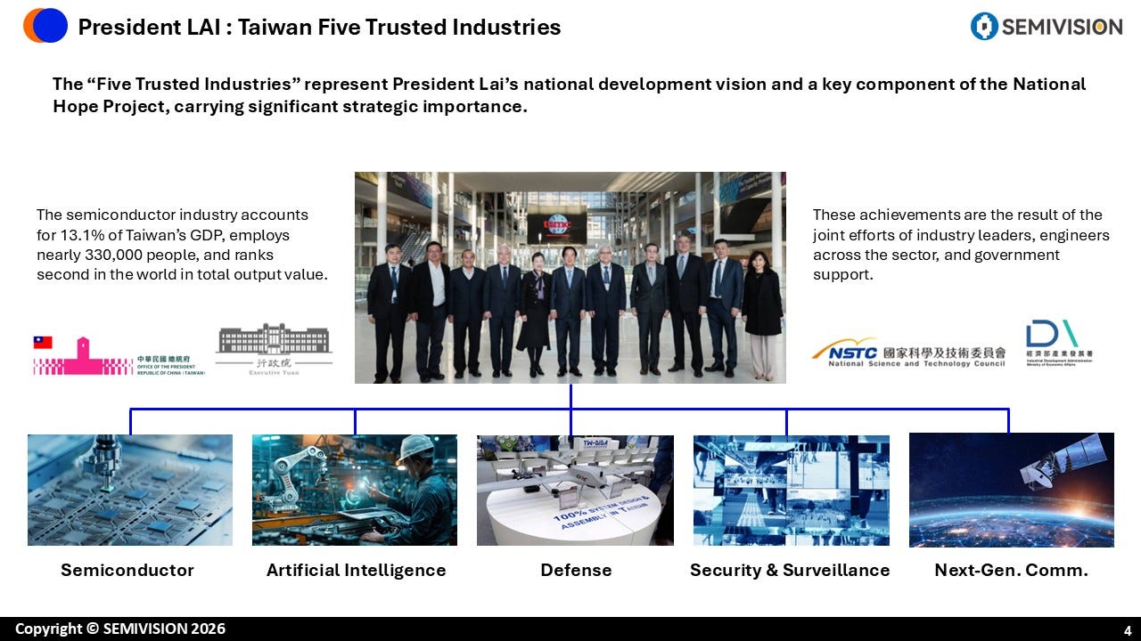
Taiwan’s government has outlined a strategic “Five Trusted Industries” initiative, focusing on semiconductors, artificial intelligence, defense, next-generation communications, and security and surveillance. Among these, the semiconductor sector stands as the cornerstone of Taiwan’s global competitiveness. It contributes approximately 13.1% of GDP, employs around 330,000 people, and ranks second worldwide in total output value. Taiwan also commands about 21% of global semiconductor manufacturing capacity, including an estimated 92% of the world’s most advanced process technologies.
Building on this strong foundation, integrated photonics is emerging as a critical next frontier. It is expected to play a key role in enabling AI, quantum computing, and future 6G communication systems. Recognizing this, the government’s strategy emphasizes strengthening IC design and R&D capabilities, expanding advanced manufacturing and pilot production, and accelerating the development of advanced packaging and materials. Enhancing supply chain resilience is also a central priority.
As global demand for high-performance computing and data infrastructure surges, integrated photonics aligns closely with Taiwan’s national strategy, positioning the country to remain a leading force in next-generation semiconductor innovation.
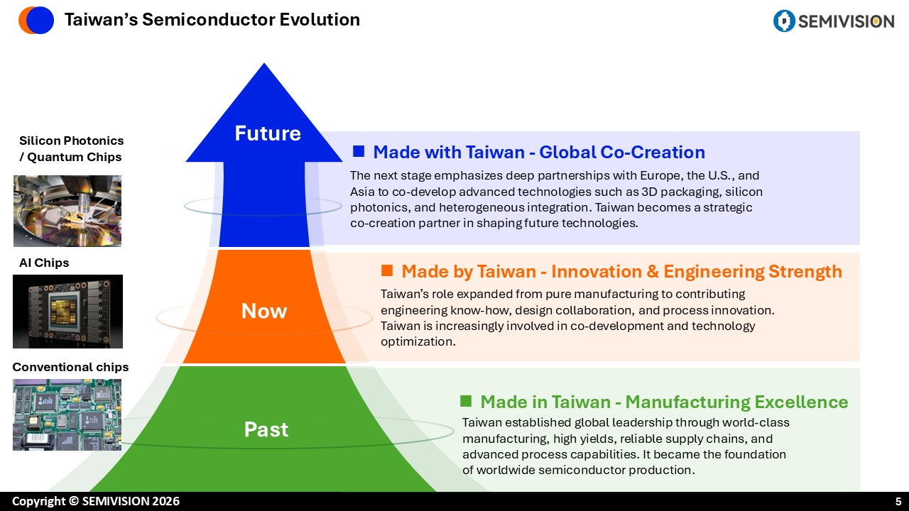
Taiwan’s semiconductor industry has evolved through three phases:
“Made in Taiwan,” where world‑class manufacturing, high yields and reliable supply chains built global leadership
“Made by Taiwan,” where roles expanded from pure manufacturing to engineering know‑how, design collaboration and process innovation; and the forthcoming
“Made with Taiwan,” which envisions deep partnerships with Europe, the U.S. and Asia to co‑develop advanced technologies such as 3D packaging, silicon photonics and heterogeneous integration. Integrated photonics exemplifies this vision because it requires holistic collaboration across design, materials, fabrication and packaging.
By partnering with the Netherlands, Taiwan can combine its strengths in high‑volume manufacturing and advanced packaging with Dutch leadership in materials and design to explore future technologies together.

The Netherlands possesses world‑leading research and technology in silicon nitride (SiN), thin‑film lithium niobate (TFLN), indium phosphide (InP), metrology and photonic design, filling critical gaps in Taiwan’s photonic integration and materials technology stack. Both sides complement one another in co‑packaged optics (CPO), silicon photonic input/output, LiDAR, biosensing, quantum and advanced photonic sensing, but must co‑develop products aimed at strong end‑markets. The Industrial Technology Research Institute (ITRI) acts as a bridge by aligning roadmaps, mapping supply chains, performing technical due diligence, validating materials/processes and scouting partners to accelerate the shift from “collaboration” to “co‑productization”. Taiwan contributes mature high‑volume manufacturing, advanced packaging and supply‑chain robustness to help Dutch PIC/TFLN/InP technologies transition from prototypes to mass production.

SemiVision has curated a selection of key and well-recognized players across the Taiwan–Netherlands photonics supply chain to provide a clear reference for the industry. Beyond these established companies, it is important to note that a growing number of startups—and even traditional players undergoing strategic transformation—are actively entering the silicon photonics space. This trend highlights the rapidly expanding ecosystem and the increasing strategic importance of integrated photonics across multiple segments of the semiconductor value chain.
If companies in Taiwan or overseas are looking to transform and enter the silicon photonics industry, we welcome you to connect withSemiVision.
We provide not only in-depth industry insights, but alsostrategic ecosystem connections—helping you engage with key players, identify opportunities, and navigate the evolving silicon photonics landscape. Through the SemiVision platform, you can gain a clearer understanding oftechnology trends, innovation pathways, and future development directionswithin the industry.
For further inquiries or collaboration opportunities, please contact:
eddyt@semivisiontw.com
jett@semivisiontw.com

TSMC’s silicon photonics platform: by integrating lasers, modulators and photodetectors on silicon and using COUPE and SoIC‑X packaging technologies, TSMC achieves high‑precision optical alignment within ±0.5 µm. Advanced thermal management with graphite lids and thermoelectric modules effectively mitigates heat accumulation under high power density, and synchronized PIC–EIC testing with automated coupling platforms establishes a comprehensive silicon photonic packaging ecosystem. This demonstrates Taiwan’s ability to realize highly integrated optoelectronic functionality on a single die, laying a foundation for future CPO and hybrid‑material platforms.

2025年7月25日
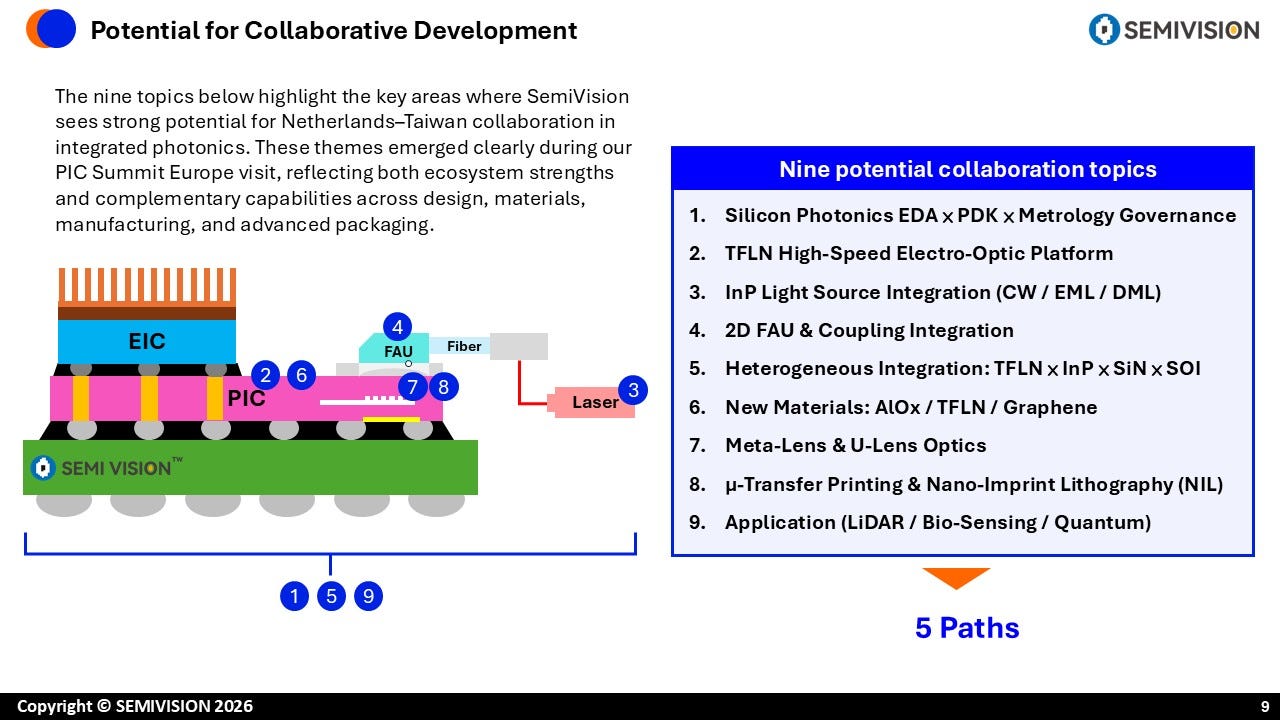

As AI/HPC optical interconnects enter the era of >200 Gb/s per lane, no single material can simultaneously deliver ultra‑low loss, high‑speed modulation and integrated light sources. A hybrid approach combining SiN (low‑loss waveguides), TFLN (>50 GHz modulation) and InP (lasers/semiconductor optical amplifiers) is emerging as a key solution.
The Netherlands has strengths in materials, photonic devices and process platforms, while Taiwan provides capabilities in 300 mm manufacturing, heterogeneous integration and advanced packaging, enabling scalable optical engines for next‑generation GPU and switch architectures. Experiments by Ciena and HyperLight demonstrated that an eight‑channel TFLN modulator chip driven by a 3 nm SerDes achieved 3.2 Tb/s PAM4 and 4.2 Tb/s PAM8 transmission over 2 km. This showcases TFLN’s high‑speed, low‑loss characteristics, making it suitable for integration with SiN and InP to build efficient optoelectronic platforms. Through collaboration, we can merge Dutch material and process R&D with Taiwan’s mass‑production, packaging and testing to establish a scalable multi‑material platform.

2025年5月15日
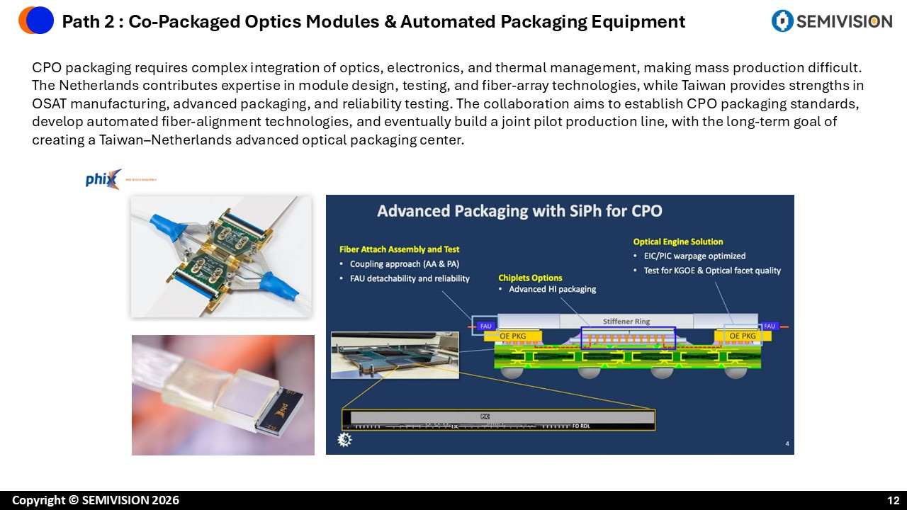
CPO packaging requires complex integration of optics, electronics and thermal management, making mass production difficult. The Netherlands contributes expertise in module design, testing and fiber‑array technologies, while Taiwan provides strengths in OSAT manufacturing, advanced packaging and reliability testing. The collaboration aims to establish CPO packaging standards, develop automated fiber‑alignment technologies and ultimately build a joint pilot production line, with the long‑term goal of creating a Taiwan–Netherlands advanced optical packaging center. This initiative will enable large‑scale CPO production and cost reduction, which is crucial for improving energy efficiency in data centers and AI servers.

2025年6月18日

Currently, fragmented process design kit (PDK) ecosystems across different material platforms cause repeated design work, unstable yields and inconsistent measurement results. Taiwan and the Netherlands can jointly establish PDK standards: in the short term, form a working group integrating SiN, TFLN, InP and packaging standards; in the medium term, build dual‑location PDK validation labs and multi‑project wafer platforms; and in the long term, develop automated optical metrology equipment. A unified PDK and EDA ecosystem will simplify design flows, improve yields and accelerate industry scaling.
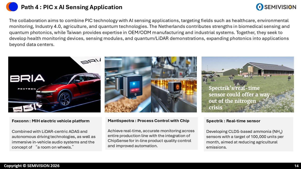
This path focuses on combining integrated photonic technology with AI sensing to open new end markets. The slide lists several examples: Foxconn’s MIH electric vehicle platform combines LiDAR‑centric ADAS, autonomous driving technologies and immersive in‑vehicle audio systems to create a “room on wheels” concept; Mantispectra uses ChipSense for real‑time quality control across entire production lines, improving automation; Spectrik is developing NH₃ sensors with a target of 100,000 units per month to reduce agricultural emissions. The collaboration aims to combine PIC technology with AI sensing in fields such as healthcare, environmental monitoring, Industry 4.0, agriculture and quantum technologies, with the Netherlands contributing expertise in biomedical sensing and quantum photonics while Taiwan provides OEM/ODM manufacturing and system integration.
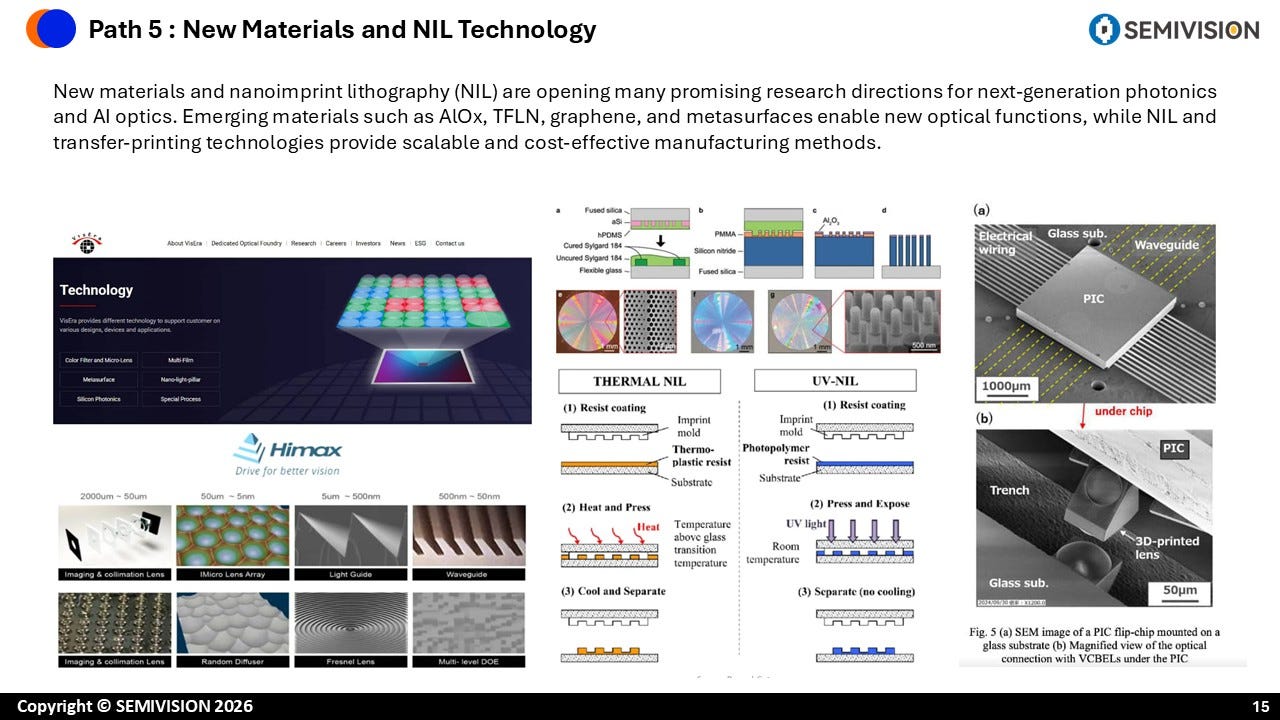
New materials and nanoimprint lithography (NIL) are opening promising research directions for next‑generation photonics and AI optics. Emerging materials such as aluminium oxide (AlOx), TFLN, graphene and metasurfaces enable new optical functions, including ultra‑thin metalenses and tunable modulators. Graphene and 2D materials provide broadband absorption and high‑speed modulation, making them promising candidates for future optical interconnects. Another key technique is micro‑transfer printing and NIL, which can cost‑effectively transfer InP or other III–V light sources onto SiN or Si substrates at high throughput, enabling heterogeneous integration for mass production. Through these material and process innovations, Taiwan and the Netherlands can jointly develop high‑performance, cost‑effective photonic components.

2025年11月29日
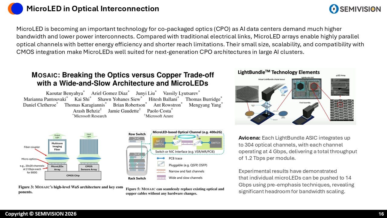
As AI data centers demand higher bandwidth and lower‑power interconnects, MicroLED is becoming increasingly important in co‑packaged optics (CPO). Avicena’s LightBundle ASIC integrates up to 304 optical channels, each operating at 4 Gbps, delivering a total throughput of 1.2 Tbps per module; with pre‑emphasis techniques, individual MicroLEDs can reach 14 Gbps, indicating significant headroom for bandwidth scaling. MicroLED arrays enable highly parallel optical channels with better energy efficiency and shorter reach limitations compared with traditional electrical links, and their small size, scalability and compatibility with CMOS integration make them well suited for next‑generation CPO architectures in large AI clusters. These advantages make MicroLED a key technology for the optical interconnect revolution in data centers.

3月20日


3月10日



2025年12月31日
Thanks for reading SEMIVISION @_@! This post is public so feel free to share it.


PreviousNext
TopLatestDiscussions








See all