Rewiring Taiwan’s Display Industry: From FOPLP to Satellite Connectivity and the Micro-LED CPO Shift
Rewiring Taiwan’s Display Industry: From FOPLP to Satellite Connectivity and the Micro-LED CPO Shift
- Source: SemiVision
- Author: SEMIVISION
- Published: 2026-03-20T18:09:17+08:00
- URL: https://tspasemiconductor.substack.com/p/rewiring-taiwans-display-industry (1) Rewiring Taiwan’s Display Industry: From FOPLP to Satellite Connectivity and the Micro-LED CPO Shift


Rewiring Taiwan’s Display Industry: From FOPLP to Satellite Connectivity and the Micro-LED CPO Shift
Original Article By SemiVision Research [Reading time: 20mins]

Mar 20, 2026
∙ Paid
A New Era Driven by AI and High-Speed Data Transmission

In recent years, the rapid rise of generative artificial intelligence (Generative AI) and cloud computing has fundamentally reshaped the semiconductor and information technology landscape. Large language models and AI accelerators require data centers to move enormous amounts of model weights and training data in extremely short periods of time. As a result, bandwidth requirements have rapidly expanded from 400 Gb/s to 800 Gb/s, 1.6 Tb/s, and even 3.2 Tb/s.
Traditional copper interconnects are increasingly becoming a bottleneck due to limitations in latency, signal attenuation, and power consumption. According to Taiwan industry report, a co-packaged optics (CPO) architecture integrating micro-LED light sources can reduce the power consumption of a 1.6 Tb/s module from about 30 W to roughly 1.6 W, representing only about 5% of the energy consumption of copper interconnects.

3月4日
As a result, a new wave of high-speed optical interconnect technologies, centered on CPO, silicon photonics, and micro-LEDs, is widely viewed as a key enabler of next-generation data centers.
For Taiwan, the traditional flat-panel display industry faces mounting pressure from the rise of mainland China’s supply chain and declining profit margins. Transformation has become urgent. This article examines how Taiwanese panel makers are expanding into advanced packaging via FOPLP, satellite communications, and micro-LED optical interconnect technologies. It explores how Innolux and AUO are moving beyond pure display manufacturing to enter fields such as satellite antennas and optical communications, while also comparing the opportunities and challenges of silicon photonics and micro-LED-based CPO technologies in the AI era.
Challenges and Transformation Drivers for Taiwan’s Panel Industry
LCD Market Saturation and Declining Profit Margins
Taiwan’s display industry experienced a golden era during the 2000s and early 2010s. However, rapid capacity expansion by Chinese panel manufacturers and the gradual saturation of the LCD television market have intensified price competition, significantly compressing average profit margins.
To find new growth engines, Taiwanese panel makers have increasingly invested in higher-value segments, including:
AMOLED displays
Automotive displays
Medical displays
Transparent display technologies
At the same time, technology integration with semiconductor manufacturing and advanced packaging has emerged as another promising pathway.
Technology Transformation: FOPLP, Micro-LED, and Satellite Communications
From a manufacturing perspective, LCD panel processes share several similarities with semiconductor fabrication, including glass substrates, driver circuitry integration, and packaging technologies. Taiwanese panel manufacturers possess deep expertise in large-area glass processing, fine metal interconnects, and high-precision patterning. These capabilities allow them to enter fields such as large-panel advanced packaging and micro-LED manufacturing.
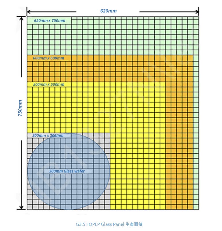
For example, Innolux is leveraging its Generation-3.5 glass production line (620 × 750 mm) to develop Fan-Out Panel-Level Packaging (FOPLP) technology. The substrate area is approximately seven times larger than a conventional 300 mm glass wafer, enabling significantly higher I/O pad density while also reducing power consumption.
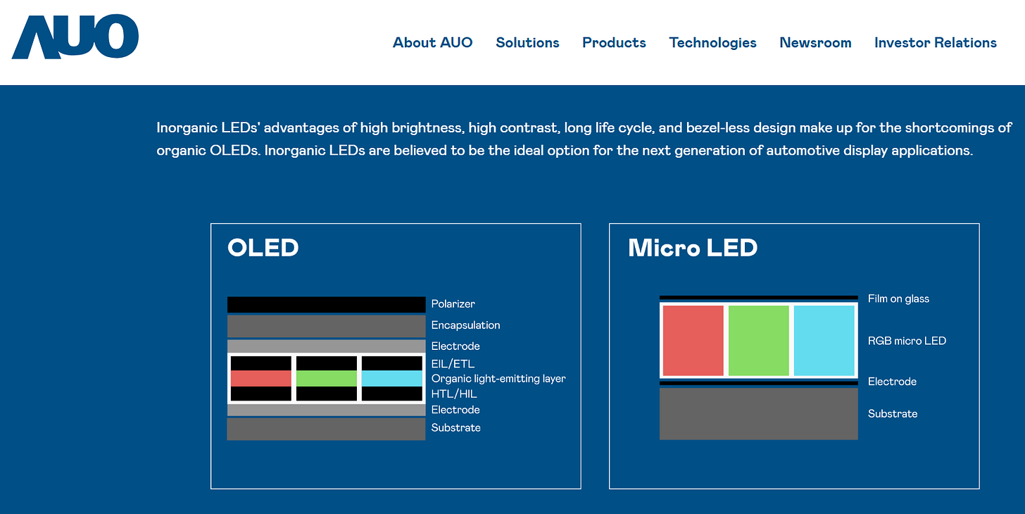
Meanwhile, AUO is extending its long-accumulated micro-LED expertise into optical communications and co-packaged optics architectures, placing micro-LED light sources on glass substrates to enable high-speed optical interconnects.
In addition, panel manufacturers are leveraging thin-film display and liquid-crystal technologies to develop flat-panel satellite antennas, expanding their reach into satellite communications and automotive V2X connectivity markets.
Below we will share:
FOPLP Technology and the Cross-Industry Expansion of Taiwan’s Panel Makers
Innolux’s FOPLP Strategy and Collaboration with SpaceX
Global FOPLP Investment and Market Outlook
Satellite Communications: Panel Makers Entering the Space Economy
AUO SatGlass and Transparent Satellite Antennas
Taiwan’s Satellite Communications Policy and Opportunities
AI Data Centers and the Demand for High-Speed Optical Interconnects
MediaTek Develops Active Optical Cable Technology with Microsoft Research to Deliver Significant Improvements in Data Center Efficiency
FOPLP Technology and the Cross-Industry Expansion of Taiwan’s Panel Makers
Origins and Advantages of FOPLP
Fan-Out Panel-Level Packaging (FOPLP) is an evolution of Fan-Out Wafer-Level Packaging (FOWLP). Traditional FOWLP relies on 300 mm circular wafers to perform Redistribution Layer (RDL) processes. While this approach offers high I/O density and thin packaging, the size of circular wafers inherently limits packaging area and throughput per production cycle.
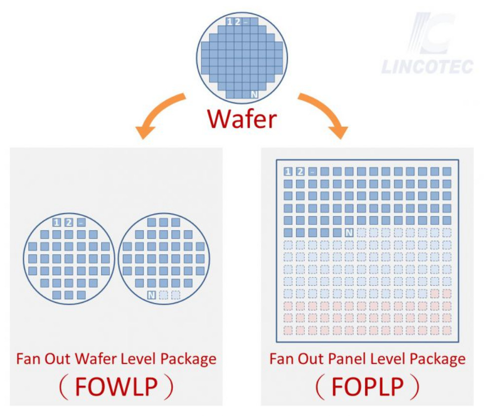
Source: Lincotec
FOPLP, by contrast, uses square panel-like substrates, similar to display manufacturing. These substrates can reach sizes of 600 × 600 mm or even 700 × 700 mm, achieving more than 95% area utilization and providing significantly larger packaging surfaces at lower manufacturing costs. Because FOPLP can accommodate more chips, offer improved thermal performance, and reduce unit packaging cost, it is increasingly viewed as a next-generation packaging option following CoWoS, particularly for AI chips, electric vehicles, and high-power computing devices.

Innolux’s FOPLP Strategy and Collaboration with SpaceX
In 2024, Innolux announced plans to convert its Generation 3.5 fabrication plant into an FOPLP production line, leveraging existing panel manufacturing equipment for semiconductor packaging processes.
According to T, Innolux originally planned to begin mass production of FOPLP in 2024. However, due to weak smartphone demand, the company shifted its focus toward automotive radar and power management ICs, which extended customer verification timelines and pushed mass production to the first half of 2025.
By Q2 2025, Innolux had begun shipping entry-level Chip-First FOPLP products, covering applications such as:
RF chips
Power management ICs
Automotive radar chips
These products are expected to generate over NT$100 million in revenue across the following three quarters. At the same time, Innolux has been collaborating with customers to develop Chip-Last packaging and TGA (Through-Glass Array) advanced packaging technologies, targeting AI and high-performance computing (HPC) applications.
Successful commercialization of FOPLP allows panel makers to engage with a broader base of semiconductor customers and lays the groundwork for future expansion into optical communications technologies.
One notable potential customer for Innolux’s FOPLP technology is SpaceX. To support vertical integration of its Starlink satellite network, SpaceX is reportedly building a 700 × 700 mm FOPLP production line in Texas. The goal is to reduce RF chip packaging costs while improving production control.
Currently, SpaceX still outsources RF chip packaging to STMicroelectronics and Innolux, but its internal investment highlights the strategic importance of FOPLP for satellite communication modules. Innolux’s experience with large-format substrates makes it a key partner before SpaceX fully completes its vertical integration strategy.
Global FOPLP Investment and Market Outlook
According to various industry reports, companies such as SpaceX (U.S.), ASE Group (Taiwan), and NVIDIA (U.S.) are actively investing in FOPLP production capabilities.
SpaceXis building a 700 × 700 mm production line in Texas while collaborating with Innolux.
ASE Groupis investing US$200 million to establish an FOPLP facility in Kaohsiung, with pilot production expected in 2026.
NVIDIAis reportedly considering the use of FOPLP in its GB200 AI accelerator platform to alleviate CoWoS capacity bottlenecks.
Market research institutions estimate that the FOPLP market will grow at a compound annual growth rate (CAGR) of 32.5%, reaching approximately US$221 million by 2028.
With its larger substrate area and lower manufacturing costs, FOPLP offers Taiwanese panel makers a potential first-mover advantage, enabling them to secure a foothold in the highly competitive semiconductor packaging market.
Satellite Communications: Panel Makers Entering the Space Economy
LEO Satellite Networks and the Data Economy
Low Earth Orbit (LEO) satellite networks are emerging as a new communications infrastructure beyond 5G and Beyond-5G (B5G) systems. Because they operate closer to Earth, LEO satellites offer lower latency and broader global coverage.
According to Morgan Stanley, the global space economy could exceed US$1 trillion by 2040.
As satellite constellations such as Starlink and OneWeb rapidly expand, companies worldwide are developing lightweight, low-cost flat-panel satellite antennas that can be integrated into vehicles, ships, and drones.
Taiwanese panel makers possess decades of experience in large-area glass processing and liquid-crystal driver technologies, capabilities that are highly applicable to the development of flat-panel satellite antennas. These technological foundations provide a natural bridge for the display industry to extend into satellite communications and space-related infrastructure.

2月9日
Innolux and Kymeta’s Liquid-Crystal Metasurface Satellite Antenna
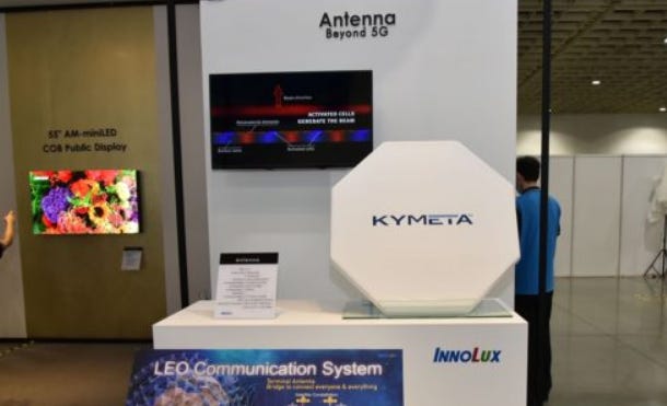
Innolux Corporation has partnered with the U.S.-based satellite communications company Kymeta to develop a liquid-crystal metasurface flat-panel satellite antenna. This antenna uses liquid crystal materials as a beam-steering medium. Unlike traditional parabolic antennas that rely on mechanical movement to track satellites, the liquid-crystal antenna can perform beam scanning by applying an external electric field to change the refractive index of the liquid crystal layer.
According to reports from Taiwan’s Institute for Information Industry (III), this type of flat-panel antenna utilizes subwavelength equivalent metasurface elements combined with liquid-crystal driving technology, enabling full-angle antenna scanning without mechanical blind spots while also reducing both thickness and cost. Technical documentation from Innolux indicates that the liquid-crystal antenna integrates thin-film transistor (TFT) panel fabrication processes, allowing phase delay in the microstructures to be modulated through bias voltage control. This mechanism enables the antenna to focus and steer electromagnetic beams electronically.
Compared with conventional satellite antennas, liquid-crystal flat-panel antennas are significantly thinner, lighter, and free of mechanical components, making them well suited for applications in vehicles, ships, and unmanned aerial systems. Taiwan’s Liberty Times further reported that this antenna does not require motors to track satellites, while offering high directivity, wide bandwidth, and low power consumption. Because the antennas can be manufactured using existing TFT-LCD production equipment, they also provide a strong cost advantage.
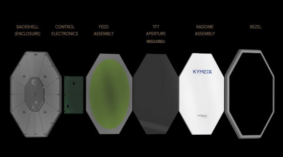
The technology has already entered markets such as luxury yachts and satellite IoT connectivity, and it was showcased to government officials during the 2020 Optoelectronics Exhibition in Taiwan.
In addition, Innolux demonstrated satellite antennas, aviation displays, and thermal imaging systems at the 2022 Taiwan Expo in the United States, signaling its ambition to enter the global satellite supply chain. Reports indicate that miniaturized satellite antennas have already entered mass production, supporting applications in LEO satellite communications, satellite IoT, autonomous vehicles, and emergency communications systems.
Innolux’s strategic push into satellite communications not only strengthens its partnership foundation with SpaceX, but also creates potential application scenarios for future co-packaged optics (CPO) optical modules and high-speed connectivity infrastructure.
AUO SatGlass and Transparent Satellite Antennas
At CES 2026, AUO introduced its innovative SatGlass Antenna, a transparent satellite communication solution developed in collaboration with YTTEK Technology. The system is based on a glass-substrate phased-array antenna architecture, allowing the antenna to be seamlessly integrated into a vehicle’s roof or sunroof glass. By embedding the antenna directly within the glass structure, the design enables satellite connectivity while keeping the external appearance of the vehicle clean and unobstructed.
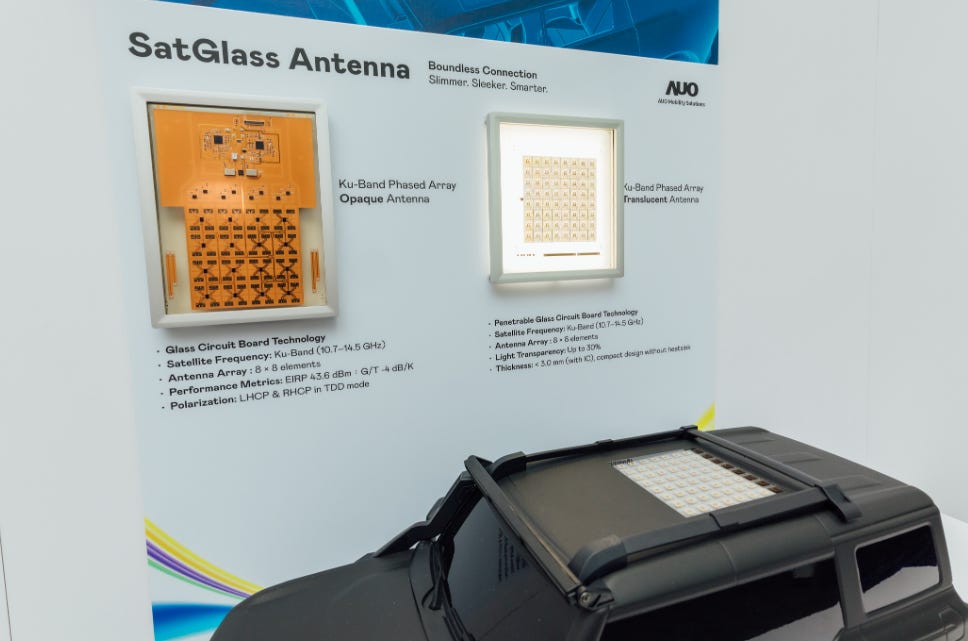
AUO highlighted that SatGlass utilizes transparent phased-array elements fabricated on glass substrates, enabling high-data-rate connectivity with Low Earth Orbit (LEO) satellite networks. The antenna supports a wide range of applications including vehicle-to-everything (V2X) communication, over-the-air (OTA) software updates, real-time navigation services, and in-vehicle streaming and infotainment. Because the phased-array system performs electronic beam steering, it can track satellites without mechanical movement, reducing system complexity while improving reliability.
From a technical perspective, SatGlass leverages AUO’s long-standing expertise in large-area glass processing, thin-film transistor (TFT) fabrication, and high-precision patterning technologies originally developed for advanced display manufacturing. By adapting these processes to produce transparent antenna arrays, AUO demonstrates how display industry infrastructure can be repurposed for next-generation communications hardware.
The concept also aligns with the broader trend of software-defined vehicles and connected mobility, where automobiles increasingly function as mobile data platforms requiring persistent high-bandwidth connectivity. Satellite links can complement terrestrial 5G and future 6G networks, ensuring global coverage in remote areas where cellular infrastructure is limited.
SatGlass represents more than just a new automotive component—it illustrates AUO’s strategic vision of merging display technologies, advanced materials, and satellite communications. By entering the LEO satellite ecosystem, AUO aims to position itself within emerging markets such as smart mobility, autonomous vehicles, satellite IoT, and aerospace communications.
Ultimately, SatGlass highlights how Taiwan’s panel manufacturers are leveraging their strengths in glass substrates, precision patterning, and large-scale manufacturing to expand beyond traditional displays and participate in the rapidly growing space and connectivity economy.

2月9日
Taiwan’s Satellite Communications Policy and Opportunities
In recent years, the Taiwanese government has promoted the “Beyond 5G Satellite Connectivity Program,” encouraging companies to invest in Low Earth Orbit (LEO) satellite communications and related components. Panel manufacturers such as Innolux and AUO are leveraging their existing display production lines to develop flat-panel satellite antennas, which helps establish a domestic supply chain for satellite terminals.
Amid growing geopolitical tensions and the ongoing U.S.–China technology competition, the ability to develop independent satellite communication technologies is becoming strategically important for Taiwan. Such capabilities can enhance national defense, disaster response, and telemedicine services, while simultaneously creating new commercial opportunities for Taiwan’s display manufacturers.
The Rise of Micro LED and Optical Communications
Evolution of Micro LED Technology and Applications Beyond Displays
Micro LED refers to arrays of light-emitting diodes smaller than 100 micrometers. These devices offer advantages such as high brightness, high efficiency, and long operational lifetime. In the display industry, micro LED is widely regarded as a next-generation display technology. However, because its pixel arrays can support high-speed modulation, micro LED has also emerged as a promising light source for optical communication systems.
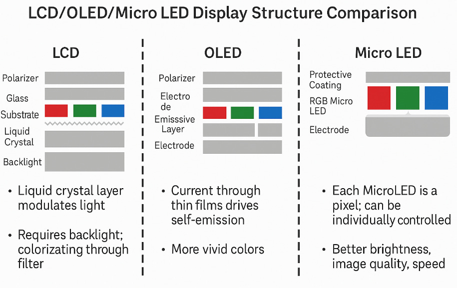
Micro LED arrays can provide tens of thousands of parallel light-emitting channels, each independently driven. This architecture is well suited for multi-core or multimode optical fiber transmission, enabling data communication with extremely low energy consumption—below 0.1 pJ per bit. Unlike traditional VCSELs or semiconductor lasers, micro LEDs typically operate in the visible light spectrum and can be integrated with CMOS driver circuits using planar manufacturing processes.
According to Taiwan industry report, micro LED-based co-packaged optics (CPO) architectures can reduce the energy consumption of optical engines to 1–2 pJ per bit, resulting in total system power consumption that is only about 5% of copper-based interconnect solutions.
Micro LED Optical Communication Modules: Principles, Prototypes, and Proof of Concept
AUO has spent many years developing micro LED display technologies and has recently extended this expertise into the field of optical communications. The company is currently developing micro LED optical communication modules, using micro LED arrays as light sources combined with glass-substrate waveguides to create high-speed optical interconnect solutions.
According to AUO, these modules are currently in the prototype and proof-of-concept (POC) stages. The company is collaborating with major players in the AI supply chain, and the technology is expected to be showcased at domestic exhibitions in the near future. AUO believes that the strong demand for low-power, high-bandwidth data transmission in AI data centers will create substantial market opportunities for micro LED-based optical interconnects.
The operating principle of these modules involves co-packaging large micro LED arrays with CMOS driver chips, with optical signals coupled through glass substrates or polymer waveguides into multi-core optical fibers. Because micro LEDs naturally exhibit a wide emission angle, micro-lens arrays or reflective structures must be added at the chip level to reduce beam divergence. Techniques such as sidewall passivation and reflective mirror structures are also used to improve quantum efficiency.
Furthermore, packaging large-area micro LED arrays requires high-precision alignment and low thermal resistance materials to maintain yield and thermal stability across tens of thousands of optical channels.
Advantages and Challenges of Micro LED Light Sources in CPO
Micro LED technology offers several advantages inco-packaged optics (CPO)applications:
Ultra-low power consumption and massive parallelism
Each micro LED channel can operate at extremely low current while supporting high-speed modulation, with energy consumption below 1–2 pJ per bit. Micro LED arrays can support tens of thousands of parallel optical channels, significantly increasing bandwidth density while reducing the need for complex SerDes architectures. Parallel optical transmission can therefore reduce both latency and power consumption.
High-temperature operation and reliability
Micro LEDs can operate reliably at temperatures exceeding 100°C, outperforming traditional VCSEL solutions. This makes them particularly suitable for co-packaged environments near high-power ASICs, where thermal conditions are demanding.
Miniaturization and optical engine integration
Micro LEDs can be vertically integrated with CMOS driver chips, and the devices can be fabricated on large glass or panel substrates, which aligns well with the manufacturing capabilities of display companies. According to Taiwan industry report, a 1.6 Tb/s micro LED-based CPO module may consume only around 1.6 watts, significantly lower than the roughly 30 watts required by conventional optical modules.

3月10日
However, micro LED CPO technology also faces several challenges:
Beam divergence and optical coupling
Micro LEDs exhibit wide emission angles, requiring micro-lenses or polymer waveguides to efficiently couple light into optical fibers. Multi-core fiber systems may also experience crosstalk. In addition, silicon waveguides have higher loss in the visible spectrum, which may necessitate the use of silicon nitride or polymer waveguide materials.
Packaging complexity and alignment requirements
Tens of thousands of micro LED emitters must be precisely aligned with driver chips and fiber arrays, making the manufacturing process complex. Double-transfer techniques or panel-level packaging processes may be required to reduce production costs.
Efficiency droop and recombination losses
At high current densities, micro LEDs can suffer from efficiency droop and sidewall recombination losses. Advanced passivation techniques and reflective structures are therefore needed to maintain both high efficiency and high-speed optical performance.
Regarding the question of whether micro LED light sources in CPO suffer from beam divergence that affects transmission efficiency, the answer is yes—micro LEDs inherently have wide divergence angles. Without optical components such as micro-lens arrays or waveguides, coupling efficiency would decrease. However, the industry is actively addressing this challenge through micro-lens integration, polymer waveguides, and silicon nitride waveguide technologies.
As for the origin of the light-source technology, AUO benefits from over a decade of experience in micro LED display development, combined with ecosystem partners such as Ennostar and PlayNitride, which provide expertise in materials and packaging technologies. This collaboration gives AUO strong capabilities in micro LED light-source development.
Regarding performance comparisons with competitors such as Credo, the technology remains in the development stage and publicly available data is still limited, making it difficult to provide objective comparisons at this time.

2025年5月4日
CPO and Silicon Photonics: Competition and Complementarity from 100G to 1.6T
Silicon photonics technology has already been widely deployed in 100G, 400G, and 800G optical modules, and the industry is now moving toward 1.6T optical interconnects. In the context of Co-Packaged Optics (CPO), two major light-source approaches are emerging: VCSEL/laser-based solutions and micro LED-based optical engines.
VCSEL technology is mature for short-distance communications, but its efficiency and temperature tolerance are generally lower than those of micro LEDs. Laser-based solutions are suitable for medium- and long-distance transmission, typically combined with silicon photonic waveguides, though they tend to consume more power. By contrast, micro LED optical engines offer low power consumption and higher thermal tolerance, making them attractive candidates for co-packaging directly with high-performance AI chips.
According to Taiwan industry report, micro LED-based CPO modules may consume only 5% of the energy required by copper interconnect solutions, attracting participation from companies such as Microsoft, Credo, Avicena, AUO, Innolux, and PlayNitride.
However, the combination of micro LEDs and silicon photonics also introduces several technical challenges. For instance, silicon waveguides exhibit relatively high optical loss in the visible spectrum, meaning that micro LED-based CPO systems may require polymer waveguides or silicon nitride waveguides instead. In addition, micro LED visible-light sources must be matched with multimode optical fibers or emerging multi-core fiber technologies to reduce signal crosstalk.
According to ASE Technology, there remains a mismatch between the bandwidth density of CPO optical engines and ASIC interfaces, which may require heterogeneous integration and panel-level packaging technologies to further increase integration density.
3月4日
Who Is Leading? Credo, Microsoft, Avicena, and Taiwan’s Panel Makers
The competitive landscape in micro LED optical interconnects is rapidly evolving, with multiple companies advancing different technological approaches.
Microsoftintroduced the MOSAIC architecture in 2024, proposing a system that uses massively parallel low-speed optical channels to reduce overall power consumption. The MOSAIC architecture integrates micro LEDs with integrated circuits, enabling a new generation of optical interconnect solutions.
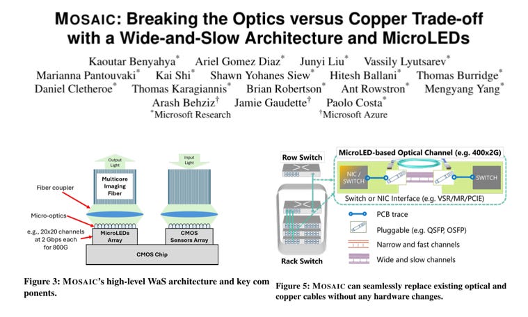
CredoTechnology acquired Hyperlume in 2025 to expand its micro LED-based optical communication technology portfolio. The company claims that this approach can provide high-efficiency, low-latency interconnects for AI data centers.
Avicenafocuses specifically on micro LED optical interconnect technologies, developing high-density optical I/O systems capable of short-range interconnects exceeding 10 Tb/s. Both Avicena and Credo emphasize that their optical engines can reduce the number of SerDes circuits, significantly lowering power consumption.

2025年6月15日
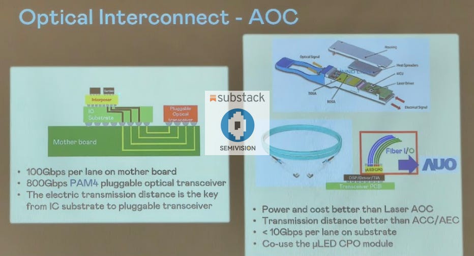
MediaTekhas announced the development of 800G and 1.6T micro LED-based Active Optical Cables (AOC) targeting short-distance intra-rack interconnects. The company highlights that micro LED arrays offer advantages over silicon photonics in power efficiency and thermal stability.
Taiwanese panel manufacturers, includingAUO, Innolux, andPlayNitride, are leveraging their strengths in micro LED design and panel manufacturing processes to enter the CPO ecosystem. Taiwan industy report reports that these companies are collaborating with international technology partners to develop micro LED optical engines and system-level solutions.
In this competitive landscape, Taiwanese panel makers hold advantages in large-format substrate processing and manufacturing scale, but they must continue advancing capabilities in optical system design, driver IC development, system integration, and international standardization.
3月10日
AI Data Centers and the Demand for High-Speed Optical Interconnects
Bandwidth and Power Challenges Driven by Generative AI
Semiconductor industry trends in 2026 indicate that ICT demand is increasingly driven by artificial intelligence, while consumer electronics demand remains weaker, leading to a divergence in market growth. IC design activity showed slight growth in Q1 2026, with AI demand driving increased adoption of advanced process nodes and memory technologies.
At the same time, geopolitical tensions and U.S.–China technology restrictions have introduced new uncertainties into global supply chains.
Within data centers, the rapid expansion of AI computing is accelerating the development of co-packaged optics. As AI clusters scale up, the demand for inter-rack bandwidth is growing dramatically. Industry projections suggest that switch bandwidth will exceed 51.2 Tb/s by 2025.
Traditional seasonal cycles in the semiconductor industry are also becoming less predictable. In Taiwan, utilization rates between 12-inch and 8-inch wafer fabs are diverging significantly, reflecting the structural transformation of the industry.

2025年7月25日
The Benefits of CPO and Micro LED Interconnects in AI Servers
As AI servers scale to tens of thousands of GPUs, interconnects between servers and network switches become a critical bottleneck.
According to Taiwan industry report, micro LED-based CPO modules can reduce the power consumption of a 1.6T optical module from approximately 30 watts to about 1.6 watts. Other reports suggest that the per-channel energy consumption of micro LED optical interconnects may be only one-tenth that of silicon photonics or VCSEL solutions.
For an AI cluster containing 100,000 GPUs, adopting micro LED-based CPO technology could save approximately 15 million kWh of electricity annually while reducing around 12,000 tons of carbon emissions. As a result, micro LED CPO is increasingly viewed as a key technology for building energy-efficient, green data centers.
The Role of Taiwanese Companies in AI Cloud Infrastructure
Taiwan hosts the world’s most advanced semiconductor foundries and packaging companies, along with a comprehensive PCB and electronics manufacturing ecosystem. In the fields of silicon photonics and micro LED optical interconnects, Taiwanese companies can play several critical roles:
- Optical Engine Manufacturers
Companies such as Innolux, AUO, and PlayNitride are leveraging their expertise in micro LED packaging and glass-substrate processing to develop optical engine modules.
- Advanced Packaging Service Providers
Companies such as ASE and TSMC are developing heterogeneous integration platforms, including VIPACK and other advanced packaging architectures, which incorporate CPO solutions to enable the co-packaging of optical engines with ASIC chips.
- System Integrators
Institutions such as ITRI (Industrial Technology Research Institute) are guiding domestic system manufacturers to develop optical interconnect switches and AI servers, while collaborating with global AI supply chains.
Together, these capabilities position Taiwan to play a critical role in next-generation AI data center infrastructure.
MediaTek Develops Active Optical Cable Technology with Microsoft Research to Deliver Significant Improvements in Data Center Efficiency

A collaborative team of researchers from MediaTek, Microsoft Research, and other suppliers have successfully designed a next-generation Active Optical Cable (AOC) powered by miniaturized MicroLED light sources. This revolutionary design of an Active MicroLED Cable can significantly improve power efficiency in data centers compared to current technologies. The use of an Active MicroLED Cable would also deliver high-reliability like copper but at a much farther reach.
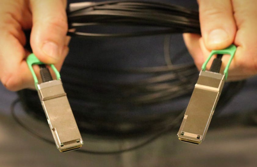
The new MicroLED cables with two transceivers attached. The transceivers contain equipment that converts photons into usable data. Photo by Chris Welsch for Microsoft.
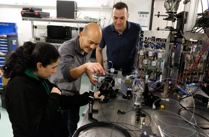
Microsoft researchers on the team that developed the new MicroLED cabling system – with one of the prototypes they used to develop the technology. Photo by Chris Welsch for Microsoft.

3月18日
Conclusion and Outlook: The Future Path of Taiwan’s Display Industry
Over the past two decades, Taiwan’s display industry has faced significant challenges due to LCD oversupply and competition from mainland China. Today, companies such as Innolux and AUO are repositioning themselves along three major strategic directions:
Advanced Packaging and Semiconductor Manufacturing (FOPLP)
Leveraging expertise in glass substrate processing and fine circuit patterning, panel makers are developing large-area fan-out panel-level packaging (FOPLP) technologies. Innolux has already begun shipping FOPLP products for RF and automotive chips and is collaborating with SpaceX, while companies such as ASE and NVIDIA are investing in large-scale FOPLP production lines.
Satellite Communications and Antenna Technologies
By developing liquid-crystal metasurface antennas and glass-based phased-array antennas, panel makers are extending their optical and circuit integration capabilities into LEO satellite terminals. Innolux’s liquid-crystal antennas developed with Kymeta are already used in luxury maritime vessels and satellite IoT, while AUO’s SatGlass enables transparent satellite antennas integrated into vehicle roofs.
Micro LED Optical Interconnects and CPO
Companies such as AUO and Innolux are expanding micro LED technology beyond displays into high-speed optical communications. Micro LED-based CPO modules have the potential to significantly reduce AI data center energy consumption while increasing bandwidth density, although technical challenges such as beam divergence, packaging complexity, and efficiency droop must still be addressed.
With strong collaboration between Taiwanese companies and international technology leaders, supported by Taiwan’s comprehensive semiconductor supply chain, micro LED CPO technologies may reach commercial deployment within the next five years.
From a global perspective, the exponential growth of generative AI and cloud services is driving unprecedented demand for high-speed optical interconnect technologies. Silicon photonics and micro LED technologies each offer distinct advantages, and they are likely to coexist and complement each other across different transmission distances and application scenarios.
The transformation of Taiwan’s panel industry therefore represents more than a product shift—it reflects a restructuring of the industry value chain, moving from pure manufacturing toward the development of core components and integrated systems.
Amid geopolitical challenges and the opportunities created by the AI era, the success of this transformation will determine the global competitiveness of Taiwan’s display industry in the coming decade.

3月16日


PreviousNext
TopLatestDiscussions








See all