From Packets to Light Paths: OCS Reshaping AI Data Center Architecture at OFC 2026
From Packets to Light Paths: OCS Reshaping AI Data Center Architecture at OFC 2026
- Source: SemiVision
- Author: SEMIVISION
- Published: 2026-03-19T12:39:45+08:00
- URL: https://tspasemiconductor.substack.com/p/from-packets-to-light-paths-ocs-reshaping (1) From Packets to Light Paths: OCS Reshaping AI Data Center Architecture at OFC 2026


From Packets to Light Paths: OCS Reshaping AI Data Center Architecture at OFC 2026
Original Article By SemiVision Research [Reading time: 25 mins]

Mar 19, 2026
∙ Paid
From Google TPU Clusters to the Optical Interconnect Era of AI Factory Networks
As generative AI and large language models (LLMs) drive compute demand to grow exponentially, traditional electrical interconnect networks are increasingly unable to support the scale and energy-efficiency requirements of next-generation AI clusters. At the 51st Optical Fiber Communication Conference (OFC 2026), AI data center optical switching—especially Optical Circuit Switching (OCS)—has emerged as a central theme, underscoring its strategic importance for AI infrastructure over the coming decade. Official OFC 2026 programming places OCS, photonic switching, and AI-cluster interconnects at the heart of its agenda, including dedicated workshops such as“Optical Networking for AI Datacenters: Technology Enablers and Key Applications”and“Photonic Switching for AI Infrastructure – Architecting the Next-Generation AI Fabric,”as well as panels on recent advances in AI cluster interconnects.

While previous-generation data centers relied primarily on packet-switched Ethernet or InfiniBand networks, these electrical fabrics are now running into hard constraints as GPU and TPU counts scale into the thousands and, increasingly, tens of thousands. The challenge is no longer only bandwidth; it is also fabric architecture, power efficiency, and system utilization. OFC 2026 explicitly frames this transition as a broader shift from conventional cloud networking toward optical technologies capable of enabling next-generation AI infrastructure. The conference’s Data Center Summit and plenary messaging both highlight hyperscale datacenter optics, AI-driven network architectures, and the urgent need for sustainable, high-capacity interconnect systems.
Semiconductor scaling and advanced 3D packaging have created unprecedented compute density, but chip-to-chip and rack-to-rack I/O bandwidth has not kept pace. This widening mismatch—often described by the industry as the I/O wall—is pushing optical interconnect ever closer to the compute and switching domains. OFC 2026’s invited and tutorial program reflects this shift directly, with talks such as “Optical Switching for AI Factories,” “Recent Advancements in Optical Circuit Switches for AI Applications,” and “Scale-Out and Scale-Up Photonic Interconnects.” Together, these sessions signal that the industry is no longer discussing optical switching as a niche research topic, but as a practical architectural lever for scaling AI systems.
Optical circuit switching offers a fundamentally different approach from electrical packet switching. By establishing reconfigurable optical paths in the optical domain, OCS can dramatically reduce the number of optical-electrical-optical (OEO) conversions, lowering latency and cutting power consumption. Unlike electronic switches, which require continuous power to inspect and process packets, optical switches consume minimal steady-state energy once a circuit is established. OFC’s official workshop description highlights these advantages explicitly, focusing on OCS use cases, performance benchmarks, orchestration strategies, and enabling technologies such as MEMS, LCoS, and silicon photonics.
This is especially relevant for AI training clusters, where communication patterns are large, repetitive, and often predictable enough to benefit from dynamically reconfigurable optical connectivity. As AI systems evolve toward “AI factories,” the network is becoming a first-order design constraint rather than a background utility. OFC 2026’s programming repeatedly uses the language of AI fabrics, AI cluster interconnects, and optical networking for AI datacenters, indicating a growing consensus that future large-scale AI systems will require a tighter integration of photonics, switching, packaging, and software orchestration.
The exhibition side of OFC 2026 reinforces that this transition is moving beyond theory into commercialization. Exhibitor announcements from companies such as DiCon, Salience Labs, and Lightelligence showcase new OCS platforms aimed squarely at AI data center applications, including MEMS-based large-port-count matrices, silicon-photonic optical switches, and distributed OCS modules embedded more directly into network architectures. These announcements point to an industry race not only around switch radix and insertion loss, but also around packaging, cost structure, and deployability in leaf-spine and AI-server connectivity topologies.
OCS is increasingly viewed as a critical candidate for the next generation of AI data center networking. It promises high bandwidth density, lower power, and a path to scaling beyond the practical limits of pure electrical switching. Based on OFC 2026’s public agenda and industry activity, the discussion is no longer whether optical switching matters, but where it will be inserted first, how it will be orchestrated with packet networks, and which device technologies will win. The following eight sections examine the architectural evolution of OCS in AI data centers, real-world deployment pathways, key enabling components, and the long-term outlook for photonic fabrics in the AI era.
We will share below,
Optical Switching in Google TPU Supercomputing Clusters
NVIDIA’s AI Factory and Optical Switching Network Architecture
Breakthroughs in Silicon Photonics and MEMS Optical Switching Technologies
PCIe-over-Optics and Composable Compute Architectures
Ultra-Large Optical Switching Matrices and AWGR Wavelength Routing Architectures
Applications of OCS in Large Language Model Training and Inference
Scalable Deployment of OCS in AI Data Centers and Expandable Network Architectures
Key Technology Trends
Conclusion: OCS as the Backbone of Future AI Networks
Optical Switching in Google TPU Supercomputing Clusters
Google has long been at the forefront of AI training hardware, and its TPU supercomputing clusters have scaled to systems containing tens of thousands of TPU accelerators per cluster. Traditional data center network topologies such as Leaf–Spine or Clos architectures achieve high bandwidth by stacking multiple layers of switches and optical transceivers. However, each additional switching layer increases power consumption, latency, and system cost, making it increasingly difficult to scale efficiently for massive AI training clusters.

To address these limitations, Google introduced optical switching technologies as early as the Jupiter data center network architecture, and later expanded their use within its Project Apollo initiative, applying Optical Circuit Switching (OCS) to TPU systems. According to statements from the Open Compute Project (OCP), Google has deployed OCS extensively within its Jupiter and AI network infrastructure. The OCP notes that “Google uses OCS technology broadly within our Jupiter and AI network architectures—including Project Apollo and TPU systems—to achieve superior performance and total cost of ownership.”
Google’s commitment to OCS has significantly influenced market expectations. In a February 2026 report, market research firm Cignal AI raised its forecast for the OCS market by more than 40%, citing Google’s TPU deployments as a key driver. The report also notes that between 2025 and 2026, the majority of available OCS ports will likely be deployed internally by Google, though the ecosystem is expected to gradually open to third-party vendors and suppliers.
The key innovation in Google’s OCS deployment lies in treating optical switching as the core of a reconfigurable optical network. This allows connections between TPU accelerators to be dynamically reconfigured during different phases of AI training. Large-scale model training typically involves communication patterns such as All-Reduce synchronization, model parallelism, and data parallelism, each of which places different demands on the network topology over time.
OCS enables the network to dynamically adjust these connections. During gradient synchronization phases, the cluster can establish global communication topologies, while in partitioned training stages it can shift to localized connectivity patterns. This dynamic reconfiguration reduces unnecessary electrical forwarding and packet queuing, lowering energy consumption while improving overall training efficiency.
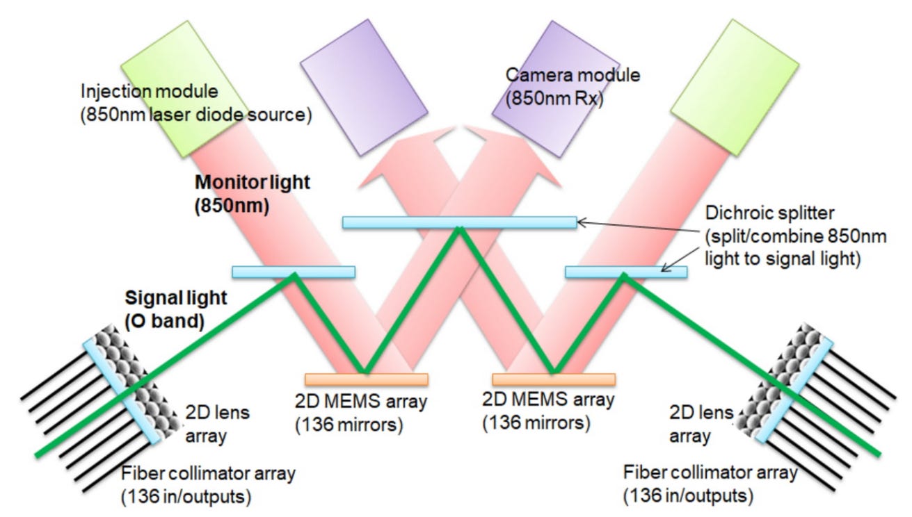
Google’s OCS infrastructure is primarily based on 3D MEMS optical switching technology. One example is the R300 optical switch introduced by Lumentum in 2025, which uses continuously tilting silicon micromirrors to precisely direct incoming optical beams toward any output fiber. The platform supports 300 × 300 ports, delivers insertion loss below 1.5 dB, and can reduce latency by up to 98% compared with electronic switching architectures.
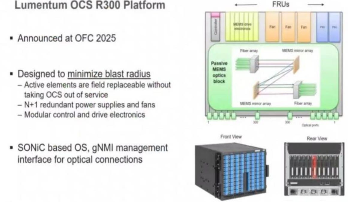
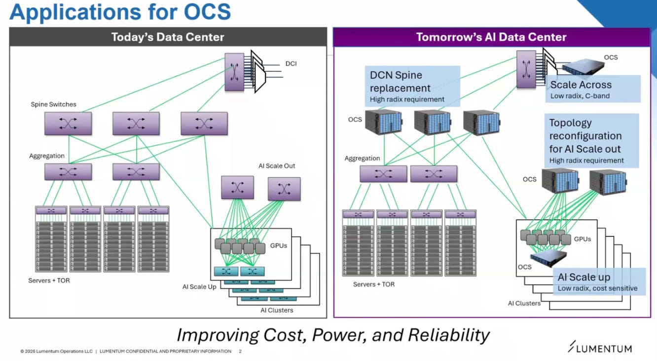
On top of this MEMS switching hardware, Google has implemented software-defined network control mechanisms to manage optical path configuration. The system leverages the open-source SONiC network operating system to orchestrate optical circuit provisioning and network management. Through this software-defined, reconfigurable optical network, large AI training workloads can dynamically utilize the interconnect bandwidth of tens of thousands of TPUs across a single cluster.
Beyond its internal deployments, Google is also helping to build a broader industry ecosystem for OCS technologies. In 2025, the Open Compute Project (OCP) and the IOWN Global Forum jointly announced the formation of an OCS sub-project, aimed at developing open interfaces and standards for optical switching systems. Google engineer Ryohei Urata emphasized that the initiative will define software interfaces based on standards such as gNMI, gNOI, gNSI, and OpenConfig, enabling interoperability across vendors and platforms.
This effort demonstrates that Google is not only leading in hardware deployment, but also actively pushing the standardization of OCS technologies across the industry. By establishing open interfaces and encouraging vendor participation, the company aims to lower barriers for adoption and accelerate the development of a broader optical switching ecosystem.

Overall, Google’s deployment of OCS within TPU clusters illustrates a major architectural shift in AI supercomputing networks—from fixed topologies toward dynamically reconfigurable fabrics. By combining MEMS optical switching hardware, software-defined control, and the Jupiter network architecture, Google is laying the foundation for the next generation of optical interconnects in large-scale AI data centers.
NVIDIA’s AI Factory and Optical Switching Network Architecture
NVIDIA has introduced the concept of the“AI Factory”to describe the next generation of AI infrastructure—where massive GPU clusters function like industrial factories that continuously produce AI models and inference capabilities. In this vision, tens of thousands or even hundreds of thousands of GPUs operate together as a coordinated computing platform. Such systems place unprecedented demands on the network, requiring extremely high bandwidth, ultra-low latency, and exceptional energy efficiency.
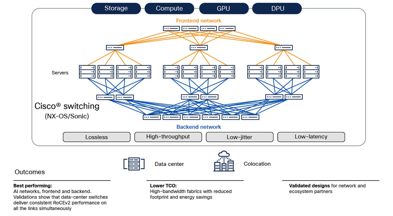
To support this architecture, NVIDIA’s ecosystem has focused heavily on GPU interconnect technologies—such as NVLink and NVSwitch—as well as high-speed optical transceivers and emerging optical switching networks.
At OFC 2026, multiple companies showcased optical interconnect technologies designed specifically for AI Factory environments. For example, Arista Networks demonstrated a 102.4 Tbps high-density 4RU switch, supporting 1.6 Tbps linear pluggable optics (LPO) with 200 Gb/s per lane, as well as fully retimed optical modules (FRO). Linear optical modules, when paired with high-quality SerDes, can reduce the power consumption associated with traditional DSP-based optical modules while achieving higher data throughput per watt.

Arista also presented a 12.8 Tbps liquid-cooled XPO module, providing extremely high bandwidth density through 64 channels × 200 Gb/s optical lanes. These demonstrations highlight a broader industry trend: the transition toward 1.6T and eventually 3.2T optical modules to meet the networking demands of AI Factory architectures.
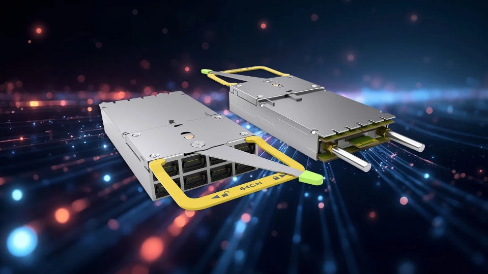
Arista : AI Datacenters are Reshaping the Optics Industry
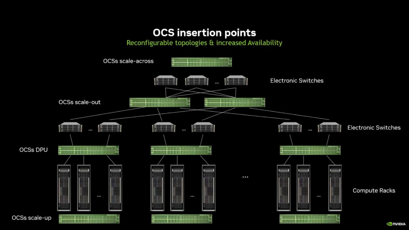
Within NVIDIA’s AI Factory framework, Optical Circuit Switching (OCS) is increasingly viewed as a complementary technology to traditional electronic switching. In existing GPU systems, NVLink and NVSwitch provide ultra-high-speed interconnects within a single server or rack, enabling all-to-all communication with extremely low latency. For communication across racks, clusters typically rely on Ethernet or InfiniBand switching fabrics.

2月26日
However, as cluster sizes grow, the power consumption and latency of electronic switching layers increase rapidly. Optical switching can serve as an additional network layer, dynamically establishing optical circuits to provide low-latency connectivity between racks or across clusters. By doing so, OCS significantly reduces repeated electrical conversions and packet queuing delays.
The advantages of optical circuit switching include:
Ultra-low power consumption:
Once an optical path is established, an optical switch consumes minimal steady-state power. This is significantly more efficient than electronic switches that must continuously operate at high speeds.
High port density and scalability:
MEMS-based or silicon-photonic OCS systems can support hundreds to thousands of ports, allowing massive GPU clusters to be interconnected through flatter and more scalable network topologies.
Extremely low latency:
Optical signals propagate through free space or waveguides without electronic buffering or packet queuing delays, enablingmicrosecond or even sub-microsecond reconfiguration times.
Software-defined reconfigurability:
Similar to NVLink and NVSwitch fabrics, OCS networks can dynamically reconfigure topology through software, assigning GPU workloads to optimized optical paths depending on the communication requirements of the training job.
NVIDIA is also exploring its own reconfigurable optical switching technologies. In various industry forums, NVIDIA representatives have discussed plans to integrate optical switching capabilities into the Spectrum-X networking platform, enabling shared control planes between electronic packet switches and optical circuit switches. This architecture would dynamically allocate optical circuits to workloads requiring extremely high bandwidth and low latency.
Although such integrated systems were not yet fully commercialized at the time of OFC 2026, NVIDIA has reportedly validated the performance advantages of OCS in internal deployments supporting large-scale AI training clusters.
The AI Factory architecture also relies on technologies such as Co-Packaged Optics (CPO) and Optical I/O (OIO) to tightly integrate compute chips with optical engines. Industry analyses indicate that these approaches aim to shorten the electrical-to-optical distance by moving optical modules closer to the compute package. Through heterogeneous integration and the use of III-V light sources, these technologies can significantly improve energy efficiency.
OCS can operate synergistically within such environments. Short-distance optical I/O links can be used for chip-to-chip communication, while OCS provides reconfigurable optical circuits for rack-scale or cluster-scale connectivity, forming a layered optical interconnect architecture.
Overall, NVIDIA’s research and ecosystem development around the AI Factory concept demonstrate the growing importance of optical switching technologies when scaling toward hundreds of thousands—or even millions—of GPUs. More broadly, they highlight a clear architectural trend: the future of AI data center networking will likely combine electronic switching with optical switching, forming hybrid electrical-optical fabrics capable of supporting the next generation of AI infrastructure.

2月28日
PCIe-over-Optics and Composable Compute Architectures
Beyond interconnects within AI training clusters, data centers are increasingly moving toward composable computing architectures. In this model, computing resources such as CPUs, GPUs, accelerators, memory, and storage are decoupled from fixed servers and instead pooled together, allowing them to be dynamically assembled through high-speed interconnects as needed. Within this context, the combination of PCIe-over-Optics technology and Optical Circuit Switching (OCS) is emerging as a key enabler for building composable infrastructure.

At OFC 2026, experimental results presented by Alibaba Cloud and Ruijie Networks demonstrated a PCIe 5.0-over-Optics architecture that integrates OSFP DR8 LPO modules with OCS switching. Their research showed that a PCIe x16 optical link using standard OSFP DR8 LPO modules can achieve error-free transmission over distances up to 100 meters, validating the scalability of fiber-based PCIe connectivity.
By deploying OCS between racks, the system can dynamically establish optical circuits between CPUs and GPUs, effectively creating a reconfigurable compute resource pool. This means that CPUs and GPUs no longer need to reside in the same physical server. Instead, they can be connected flexibly across racks—or even across entire data center halls—allowing resources to be composed on demand. Such architectures enable more efficient hardware utilization, easier maintenance, and greater operational flexibility.
The combination of PCIe-over-Optics and OCS offers several key advantages:
Resource pooling and dynamic scheduling:
Through dynamically configurable optical paths, CPUs and GPUs from different servers can be temporarily assembled into logical “compute nodes,” improving overall hardware utilization.
Extended interconnect distances:
Traditional PCIe connections over copper cables are limited by signal attenuation and cable length. Optical interconnects significantly reduce loss and latency, enabling rack-to-rack distances of tens or even hundreds of meters.
Reduced power consumption and improved thermal efficiency:
By minimizing electrical cabling and intermediate switching devices, optical connectivity reduces both power consumption and cooling requirements.
However, PCIe-over-Optics combined with OCS still faces several technical challenges. These include the cost of optical modules, physical-layer error recovery mechanisms, and the complexity of software orchestration. Experimental studies indicate that when PCIe topologies are dynamically controlled by OCS, compatible hot-plug procedures and resource management frameworks are required to prevent device identification issues during reconfiguration.
Despite these challenges, current research demonstrates that optical interconnects can successfully transport traditional I/O protocols, providing a promising foundation for future composable computing systems. As data centers continue to scale and workloads become more heterogeneous, technologies such as PCIe-over-Optics and OCS may play a central role in enabling flexible, high-performance compute resource pooling across next-generation AI infrastructure.
Breakthroughs in Silicon Photonics and MEMS Optical Switching Technologies
For Optical Circuit Switching (OCS) to be deployed at scale in AI data centers, the performance and cost of core optical components are critical factors. At OFC 2026, the convergence of silicon photonics integration and MEMS technologies emerged as a key direction for the evolution of OCS systems.
Silicon photonics enables the integration of optical waveguides, modulators, couplers, and photodetectors on silicon chips using CMOS-compatible fabrication processes, providing high levels of integration and lower manufacturing costs. MEMS technology, on the other hand, employs micro-electromechanical mirrors or reflectors to steer optical beams through free space toward the desired output ports. This approach offers low power consumption, precise optical beam control, and high switching accuracy.
According to Lumentum’s technical blog, two major products in its MEMS OCS portfolio—the R300 released in 2025 and the R64 series introduced later that year—represent significant advances in optical switching platforms. The R300 uses a three-dimensional MEMS mirror array to enable 300 × 300 optical cross-connect ports with an insertion loss of only 1.5 dB, meeting the optical budget requirements for modules such as FR4, DR4, and ER4. Compared with electronic packet switching, MEMS-based optical paths can reduce latency by up to 98%. In addition, the platform supports ultra-wideband operation across O, C, and L wavelength bands, offering protocol- and data-rate-agnostic connectivity. The system control software is built on the open-source SONiC networking platform, allowing OCS systems to integrate with existing data center management infrastructures.
At OFC 2026, startup nEye Systems presented an invited talk on the design of high-port-count silicon-photonic MEMS OCS systems. Their architecture integrates MEMS reflective elements directly onto silicon photonics chips, creating highly integrated optical switching modules. This integration significantly reduces system size, improves switching speed, and minimizes fiber coupling losses, thereby increasing the scalability of OCS platforms. Moreover, because silicon photonics is compatible with CMOS manufacturing processes, it enables mass production and potential cost reductions, making large-scale deployment of OCS more feasible.

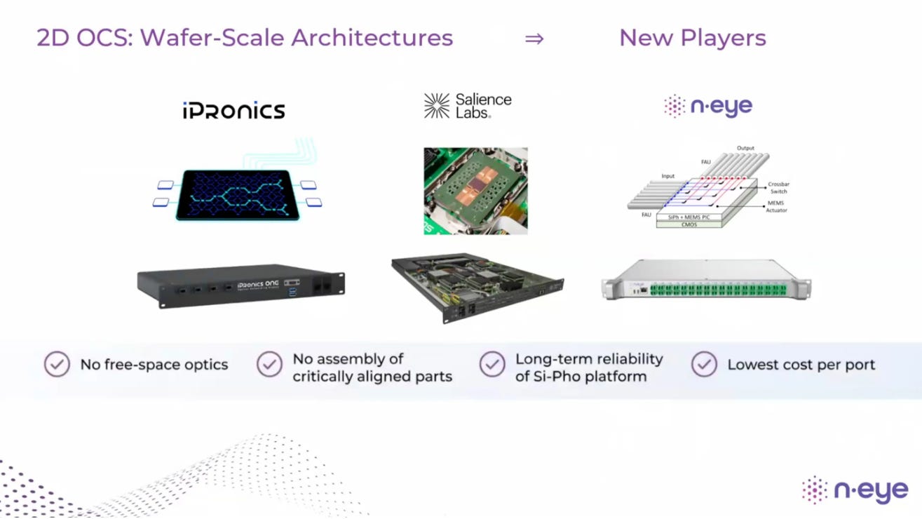
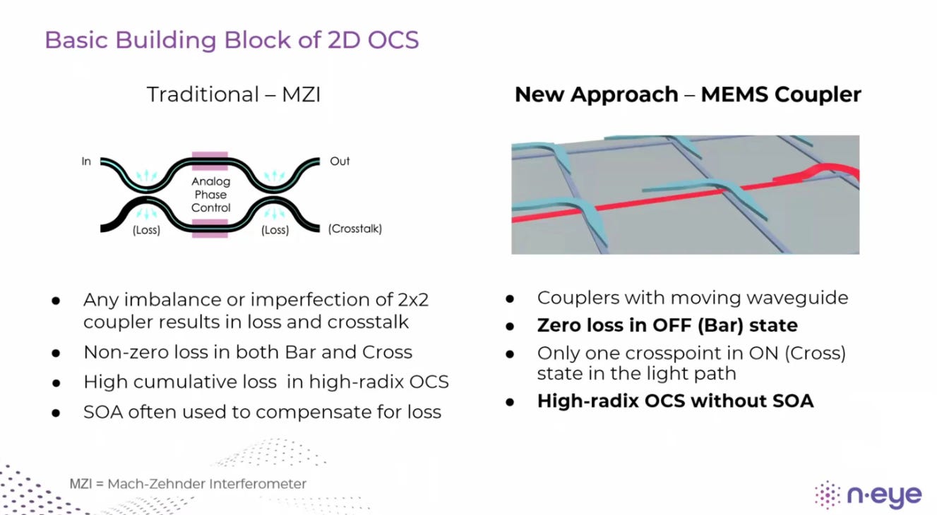
Beyond MEMS-based architectures, silicon photonics itself is enabling new forms of reconfigurable optical switching devices. For example, research teams from the University of Cambridge and Ghent University have developed bendable directional couplers that combine Mach–Zehnder interferometers (MZIs) with curved waveguides. This design achieves ultra-low crosstalk and low insertion loss within a compact footprint and has been demonstrated in 4 × 4 silicon photonic switching matrices.
Researchers from the National University of Singapore have proposed pixelated nano-opto-electro-mechanical (NOEM) gratings, capable of achieving nanosecond-scale reconfiguration speeds and over 100 nm of wavelength tuning bandwidth. These devices are suitable for on-chip wavelength-selective switching and optical spectral shaping applications.
Meanwhile, the University of California, Santa Barbara (UCSB) has demonstrated an O-band 2 × 2 × 2λ silicon photonic wavelength selective switch (WSS) featuring polarization diversity. The device achieves an extremely low polarization-dependent loss of just 0.41 dB, highlighting the potential of silicon photonics to deliver high-performance switching solutions.
Beyond MEMS and silicon photonics architectures, some research efforts are exploring new actuation and fabrication techniques. Researchers from the KTH Royal Institute of Technology in Sweden, Tyndall National Institute, and imec have proposed a non-volatile MEMS switching approach combined with post-processing fabrication techniques. By reducing the initial MEMS gap from 230 nm to 50 nm, this method allows optical MEMS devices to surpass conventional photolithography resolution limits. The result is tighter waveguide coupling and lower insertion loss, enabling higher-performance optical switching devices.
Taken together, these innovations suggest that OCS technologies will continue pushing the boundaries of port density, switching speed, and energy efficiency in the coming years. Advances in silicon photonics and MEMS integration are laying the technological foundation necessary for large-scale deployment of optical switching fabrics in future AI data centers.

3月4日
Ultra-Large Optical Switching Matrices and AWGR Wavelength Routing Architectures
As AI training clusters scale to tens of thousands or even hundreds of thousands of accelerators, optical switching systems must support thousands of ports to maintain efficient connectivity. At OFC 2026, multiple research groups and industry participants presented architectures for ultra-large Optical Circuit Switching (OCS) systems. The dominant technological approaches combine spatial routing with wavelength routing, as well as passive wavelength routing using Arrayed Waveguide Grating Routers (AWGRs).
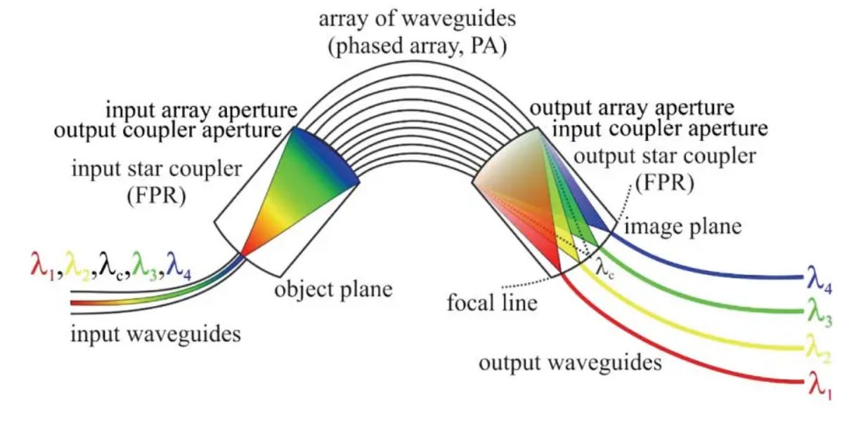
Researchers from Nagoya University in Japan proposed a 4096 × 4096 fully non-blocking OCS architecture that uses star couplers to avoid the cascading loss typically associated with multi-stage switching networks. By integrating spatial and wavelength routing mechanisms, the design achieves an overall switching capacity of 819.2 Tb/s. This architecture demonstrates that a single-layer switching fabric can support up to 4096 ports, highlighting the scalability of OCS for extremely large AI clusters. Through carefully designed optical path allocation and wavelength routing schemes, the system can provide full connectivity while maintaining acceptable insertion loss.
Another notable architecture was presented through a collaboration between the University of California, Davis, Lawrence Berkeley National Laboratory, and Enablence Corporation. Their system, known as Thin-CLOS-LION, implements a 1024 × 1024 fully interconnected optical switching fabric based on 64 × 64 uniform-loss AWGR devices. AWGRs exploit the interference properties of different wavelengths within optical waveguides to route input wavelengths to specific output ports in a deterministic order. As a result, they function as passive wavelength-routing components.
In experimental demonstrations, the research team showed that the system could achieve full interconnection through 64 wavelength channels, with a total system insertion loss of approximately 7.5 dB and crosstalk of −24 dB. Because AWGR devices are passive and require no active switching power, they offer extremely low power consumption. Furthermore, their ability to operate within single-layer or minimal-layer switching architectures makes them particularly attractive for ultra-large optical switching matrices.
Another key enabling technology is the Wavelength Selective Switch (WSS). Researchers from the Eindhoven University of Technology and Huawei’s German Research Center demonstrated an O-band 4 × 4 × 8λ WSS architecture. The device uses a 400 GHz, 8-channel flat-top arrayed waveguide filter combined with a semiconductor optical amplifier (SOA) array, enabling polarization-independent wavelength switching.
The experimental system achieved an insertion loss below 3.5 dB, crosstalk lower than −37 dB, and demonstrated 100 Gb/s PAM4 transmission with only 0.8 dB penalty. Such devices can function as modular components within larger OCS networks, enabling fine-grained wavelength allocation and dynamic optical resource management.
Overall, research into ultra-large OCS architectures suggests that combining spatial routing, wavelength routing, and AWGR-based technologies can enable switching systems with thousands or even tens of thousands of ports within relatively flat network structures. These flattened architectures reduce the number of switching stages, significantly lowering latency and energy consumption—both of which are critical for next-generation AI supercomputing clusters and hyperscale data centers.
Applications of OCS in Large Language Model Training and Inference
Training large language models (LLMs) requires extensive data synchronization and communication among thousands of GPU or TPU nodes. In traditional electronic switching networks, packet queuing and buffering introduce additional latency, which can limit overall training efficiency. Optical Circuit Switching (OCS) can address this challenge by providing dedicated optical paths for these communication patterns, avoiding packet contention and congestion while enabling reconfigurable network topologies that adapt to different training phases.

Researchers from the University of Cambridge and imec have proposed a training-phase-aware OCS architecture, in which the optical network topology dynamically adjusts based on the stage of model training—such as forward propagation, backpropagation, and gradient synchronization. In this approach, OCS establishes the most suitable optical connectivity pattern for each phase of computation. Experimental results show that, compared with static optical networks, this scheme can improve communication efficiency by approximately 37.5% under standard LLM training configurations. Such improvements can significantly shorten training time, particularly in multi-tenant environments or mixed training workloads.
For inference workloads, the reconfiguration speed of OCS also plays a critical role in determining system performance. Analysis from researchers at the University of California, Berkeley, in collaboration with Ayar Labs, suggests that when high fan-out communication is not required, OCS can outperform conventional electronic switching networks only if the reconfiguration time is below approximately 700 nanoseconds. However, in scenarios involving high fan-out communication patterns—such as broadcast operations—OCS remains competitive even with slower reconfiguration speeds. These findings provide clear performance targets for the design of next-generation OCS devices.
Meanwhile, researchers from the University of Chinese Academy of Sciences proposed a hardware-accelerated OCS scheduler called HOCSS. In optimal conditions, the system achieves port-matching latency below 1 microsecond, delivering a 68.8× speed improvement compared with software-based scheduling implementations. These results suggest that combining OCS with hardware-accelerated scheduling and training-phase-aware network control can significantly improve both the training and inference efficiency of large language models.
Additional research from Japan’s National Institute of Advanced Industrial Science and Technology (AIST) demonstrated the use of 4 × 4 silicon photonic switches to perform fully optical All-Reduce operations, which are fundamental collective communication primitives in distributed AI training. The researchers also proposed using OCS to dynamically switch between different parallel training strategies—such as Mixture-of-Experts (MoE), tensor parallelism, and data parallelism—with additional switching overhead kept below 2 microseconds.
These studies indicate that future AI clusters may evolve toward fully optical compute-and-switch architectures, where OCS not only enables high-performance data movement but also supports optical collective operations. Such systems could significantly improve both energy efficiency and scalability for next-generation AI infrastructure.
Scalable Deployment of OCS in AI Data Centers and Expandable Network Architectures
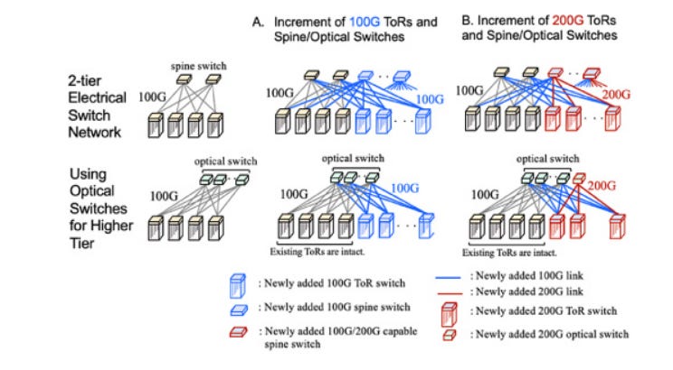
Deploying Optical Circuit Switching (OCS) in AI data centers is not merely a hardware challenge. It involves system-level considerations including network topology design, resource scheduling, energy efficiency, and inter–data center connectivity. Insights from OFC 2026 and related research highlight several key strategies for scalable deployment:
Flow-Level Control and Dynamic Scheduling:
Researchers from Beijing University of Posts and Telecommunications and the China Unicom Research Institute proposed a flow-level control system for hybrid optical-electrical networks. By monitoring traffic in real time and dynamically configuring OCS based on communication demands, the system demonstrates significant performance gains. Results show a50.3% reduction in All-Reduce latency, a47.1% increase in bandwidth utilization, and a32% reduction in power consumption. This indicates that with intelligent control planes and fine-grained traffic management, OCS can substantially improve both efficiency and energy performance in real-world deployments.
Scalable Inter–Data Center Architectures:
KDDI Research in Japan proposed an architecture that leverages OCS to establish optical paths across distributed clusters. This approach supports transmission distances exceeding 30 km without degrading AI job completion time. The implication is profound: future AI superclusters do not need to be confined within a single data center, but can instead be distributed across multiple campuses. With OCS combined with appropriate coherent transmission technologies, inter–data center networks can achieve both high bandwidth and low latency simultaneously.
Dual Resource Pooling Architecture:
Shanghai Jiao Tong University introduced the ocs-DRP (Dual Resource Pooling) architecture, which uses OCS to create both intra-rack and inter-rack resource pools, forming a flatter AI data center network. Compared to traditional fat-tree architectures, ocs-DRP achieves similar latency performance while reducing power consumption by up to 40%. This suggests that resource pooling and flattened network topologies will become key trends in next-generation AI data centers, with OCS serving as a foundational enabler.
Physical Layer Automation and Fiber Management:
Telescent has developed a high-density robotic cross-connect system designed to manage the massive volume of optical fibers in AI GPU clusters. This system uses robotic automation to configure and reconfigure fiber paths, supporting parallel optical interconnects such as DR4 and DR8. It helps reduce human wiring errors and significantly shortens deployment time. When integrated with OCS control systems, such physical-layer automation can greatly simplify large-scale deployment while improving reliability.

Taken together, these strategies highlight that scaling OCS in AI data centers requires a coordinated evolution across hardware innovation, software-defined control, and system-level architecture design. Research institutions and industry players worldwide are actively exploring diverse topologies and control frameworks to meet the performance and energy efficiency demands of hyperscale AI clusters.

Future Outlook: The Role and Trends of OCS in AI Compute Networks
Insights from OFC 2026 and broader industry developments indicate that optical switching is transitioning from research to commercial deployment, and is poised to play a central role in future AI infrastructure. The next-generation network architecture is likely to adopt alayered structure:
Intra-chip / In-package Interconnects:
Technologies such as UCIe, CXL, and CPO/OIO will tightly integrate compute chips with optical engines, enabling high-bandwidth, low-power short-reach interconnects. SemiVision highlights that 1.6T and even 3.2T optical modules, along with CPO, were key focal points at OFC 2026—signaling the industry’s push toward deeper integration between optics and electronics.
Intra-rack Interconnects:
High-speed Ethernet or InfiniBand will likely remain dominant in the near term. However, as data rates continue to scale, Linear Pluggable Optics (LPO) and silicon photonics-based modules are expected to gradually replace copper interconnects.
Rack-to-rack / Cluster-level Interconnects:
Inter–data center Interconnects:
By leveraging coherent optical transmission, OCS, and composable architectures, future AI supercomputing networks can span multiple campuses or even cities, forming distributed, large-scale compute fabrics.
Key Technology Trends
According to OFC 2026 and related reports, several major trends are emerging:

Source: Huawei
Rapid Growth of 1.6T and 3.2T Optical Modules:
The industry is transitioning from 800G to 1.6T, accelerating the maturity of linear optics and CPO technologies. Experimental validation of 3.2T modules may follow. These ultra-high-speed optical links will work in tandem with OCS to enable high-density, high-throughput networks.
Heterogeneous Integration in Silicon Photonics and New Light Sources:
Research is advancing the integration of silicon photonics with materials such as TFLN (thin-film lithium niobate) and III-V semiconductors, improving modulation efficiency and bandwidth. At the same time, emerging light sources such as VCSELs and microLEDs are being explored for short-reach optical interconnects.
AI-Driven Network Control and Automation:
AI is increasingly being applied to network operations, enabling predictive monitoring, traffic optimization, and topology adaptation. Adtran describes AI as forming an “optimization loop” from PIC design to real-time network operation. When integrated with OCS control planes, this can significantly enhance network performance and reliability.
Next-Generation Fiber and Spatial-Domain Technologies:
Hollow-core fiber (HCF) has emerged as a key topic at OFC 2026, offering low dispersion and low loss characteristics that may benefit long-distance data center interconnects. Additionally, satellite optical communications and space-based optical networks are gaining attention, indicating that optical interconnects may extend beyond terrestrial infrastructure.
Open Ecosystems and Standardization:
The Open Compute Project (OCP) has initiated an OCS subproject to define open hardware and software interfaces. Participation from companies such as Google and Microsoft reflects a strong industry push toward standardization—reducing supply chain fragmentation and enabling interoperability across vendors.
Conclusion: OCS as the Backbone of Future AI Networks
Taken together, OCS is evolving from a proprietary solution into an open ecosystem technology, converging with CPO/OIO, silicon photonics, and AI-driven control systems.
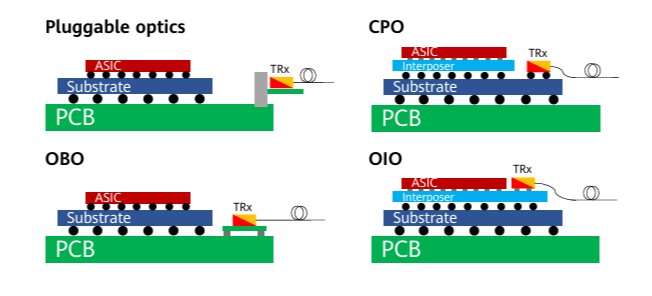
Optical interconnection modules and engines in different modes (Source: Huawei)
Future AI data centers are likely to adopt a three-layer hybrid optical-electrical architecture:
Intra-accelerator interconnects
Intra-rack interconnects
Rack-to-rack and inter–data center interconnects
Within this structure, OCS will serve as the core backbone of the third layer, enabling scalable, energy-efficient, and dynamically reconfigurable networks.
With ongoing deployments by hyperscalers such as Google, NVIDIA, and Alibaba Cloud, along with continuous advancements from silicon photonics and MEMS-based switching companies, optical switching is steadily moving from research into real-world implementation.
OFC 2026 makes one trend unmistakably clear:
optical switching is reshaping AI infrastructure and laying the foundation for the next generation of compute networks built on optical interconnects.
Thanks for reading SEMIVISION @_@! This post is public so feel free to share it.
Reference information
Multiple OCS suppliers are set to showcase their latest technologies and products at OFC 2026.
In 2025, Optical Circuit Switching (OCS) gained significant attention as Google expanded its deployment, and it is increasingly regarded as a key technology for future AI data center networking. Based on currently available information, several OCS vendors will be participating in OFC 2026 and presenting their newest solutions.

https://www.coherent.com/networking/optical-circuit-switch

https://www.lumentum.com/en/products/300x300-optical-circuit-switch-ocs
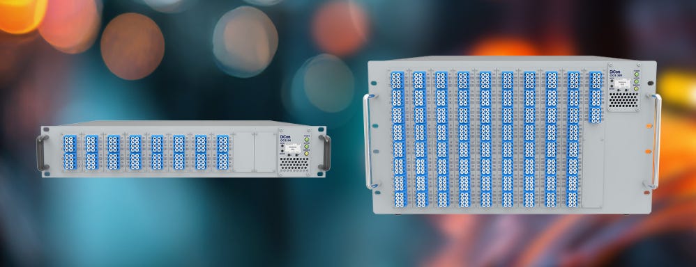
DiCon Announces Two Value-Focused Optical Circuit Switches (OCS) for AI Data Centers and Celebrates 40 Years of Photonics Excellence
DiCon Fiberoptics, Inc. announces the expansion of its MEMS Optical Circuit Switch (OCS) portfolio by introducing the highly reliable and value-focused 300x300 and 64x64 models, designed for data center leaf-and-spine networks and AI server torus connectivity architectures.
These 2 Optical Circuit Switches are built with the same DiCon 3D MEMS platform and carry the same proven reliability as DiCon’s field deployed 384x384 Optical Matrix Switches. To reduce the cost (and pass on the savings to end-customers) the 2 new models have less premium features and do not offer many advanced options. The end-to-end loss through the OCS is less than 3.0 dB, meeting the requirements set by the hyperscalers and data center operators.
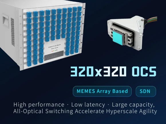
Accelink Technologies will conduct a live demonstration of its 320×320 OCS system at OFC 2026.
With 320 input/output ports, the system supports more complex leaf-spine interconnect architectures and supernode cluster communications, creating dedicated “light-speed pathways” for AI training workloads. By eliminating latency jitter caused by O/E/O conversions, it ensures stable communication patterns, enables flexible compute resource pooling and scheduling, and ultimately improves training efficiency.

Eoptolink Demos Its NX200 and NX300 Series Optical Circuit Switching (OCS) Solution at OFC 2026
Eoptolink’s OCS switches, the NX200 and NX300, support 140 ports and 320 ports respectively, enabling optimized AI network architectures at different scales.
At the heart of both the NX200 and NX300 systems are Eoptolink’s self-developed MEMS (Micro-Electro-Mechanical Systems) mirrors, which physically steer light beams to create direct, reconfigurable optical paths between network endpoints. This approach eliminates power-intensive optical-electrical-optical (O-E-O) conversions at each network hop, delivering several key benefits:
Significantly reduced network power consumption
Lower and more predictable latency
Improved GPU utilization and shorter training cycles
Reflecting Eoptolink’s commitment to open networking, the NX series is powered by the Eoptolink OCS Operating System, developed as a SONiC-compliant platform. As an active member of the Open Compute Project (OCP), Eoptolink has joined the Optical Circuit Switching (OCS) project and is committed to contributing to the development and standardization of OCS technologies.

At OFC 2026, TeraHop will live-demonstrate:
The industry 1st 12.8T-8xDR8 XPO optical transceiver module, delivering the highest capacity to support next generation AI scale up
The industry 1st 6.4T-4xDR8 Pluggable NPO module with high density and low power for AI scale up
The industry 1st 4x400G Optical transceiver module to demonstrate feasibility of next generation 400G per lane optics for 3.2T
The industry 1st 1.6T- 2x LR4 OSFP and 800G-LR2 coherent lite optical transceivers for scale across multiple AI data-center buildings
Joint demo of 1.6T- DR8 OSFP optical transceivers with Nvidia DSP
64x64 and 300x0300 MEMS-based optical circuit switch (OCS) systems to enable lower power data-center networking, and reconfigurable AI compute fabrics
PCIe 6 AOC and AEC
In addition, there will be live demonstration of TeraHop product solutions with industry parties and standards bodies:
The industry 1st Multi-core fiber (MCF) native 1.6T-2xDR4 OSFP optical transceiver as a joint live demo with Corning at booth #1739
MCF-native 800G-2xDR4 OSFP, 1.6T-2xDR4 FRO, RTLR, LPO optical transceivers at OIF inter-op demonstration booth # 2017
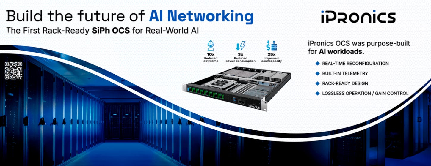
IPRONICS TO SHOWCASE PROGRAMMABLE PHOTONICS LEADERSHIP AT OFC 2026
At OFC 2026, iPronics will showcase the first commercially available Silicon Photonics (SiPh) Optical Circuit Switch (OCS), available in different radix configurations as part of the ONE Series. The company will demonstrate the device’s high performance and its ability to dynamically switch connectivity across multiple ports to optimize AIcluster interconnects.
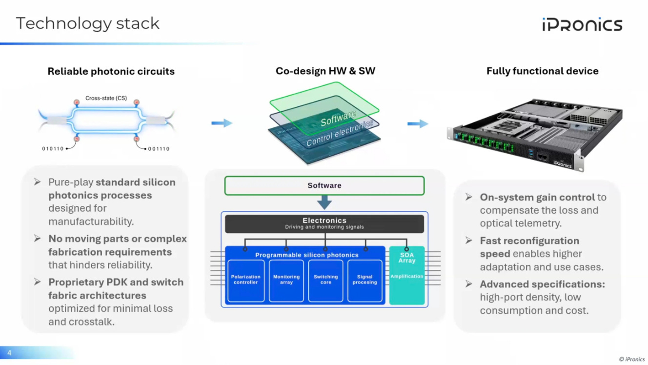
Powered by softwaredefined control, the ONE Series enables reconfigurable, lowlatency Layer 1 topologies for AI workloads. Compared with MEMSbased switching, SiPh delivers faster reconfiguration times, a smaller form factor, and a path to lower cost at scale. It also enables integration of additional onchip functions—such as telemetry via monitoring photodetectors—while providing a clear scalability path when higher performance and larger radix are required.

Salience Labs Launches Industry’s Highest Performing 32-Port All-Optical Silicon Photonic Switch to Transform the Networking Layer of AI Datacenter Infrastructure
Salience Labs’ all-optical switch technology improves network latency, throughput and reliability metrics while lowering power consumption. The 32-port product is the first product in Salience Labs’ suite of all-optical circuit switch (OCS) solutions, which also includes 64- and 128-port technologies to meet the evolving capacity and bandwidth needs of next-generation AI datacenters.

2025年5月13日
Oriole announced PRISM Ultra, the next major evolution of its pure photonic‑ AI networking platform. PRISM (Photonic Routing for Scalable Models) has solved long-standing challenges in nanosecond speed optical circuit switching, transceiver synchronization and control. PRISM Ultra, building on PRISM foundations, introduces a step change in performance, scalability, energy-efficiency and system architecture for the next generation of AI data centers.
PRISM Ultra is the next evolution and a new architecture for frontier-scale AI
PRISM Ultra merges scale-up bandwidth with scale-out connectivity, delivering unmatched bandwidth, including:
51.2 Tb/s per xPU across 1,000 zero-hop nodes
180ns xPU to xPU latency
One-hop contention-free connectivity extending to one million nodes


PreviousNext
TopLatestDiscussions








See all