NVIDIA: Co-Packaged Optics at a Crossroads: Narrow & Fast vs. Wide & Slow
NVIDIA: Co-Packaged Optics at a Crossroads: Narrow & Fast vs. Wide & Slow
- Source: SemiVision
- Author: SEMIVISION
- Published: 2026-03-18T09:14:25+08:00
- URL: https://tspasemiconductor.substack.com/p/nvidia-co-packaged-optics-at-a-crossroads (1) NVIDIA: Co-Packaged Optics at a Crossroads: Narrow & Fast vs. Wide & Slow


NVIDIA: Co-Packaged Optics at a Crossroads: Narrow & Fast vs. Wide & Slow
Original Article By SemiVision Research [Reading time: 12 mins]

Mar 18, 2026
∙ Paid
Optical Interconnects in AI Factories: Narrowband High-Speed vs. Wideband Low-Speed — A Technology Path Analysis

Background: AI Factories, Scale-Up/Scale-Out, and the Power Bottleneck
With the rise of generative AI and large language models, the scale and power consumption of computing clusters have grown explosively in recent years. Traditional enterprise data centers typically adopt a CPU-centric architecture, where Tier-1 switches are located within each server rack, and servers connect to the switches through short-distance copper cables. In this model, both power consumption and connection complexity remain relatively manageable.

3月17日
However, in an“AI factory”, thousands of GPUs must operate together like a single supercomputer. This dramatically increases the requirements for bandwidth and latency. Tier-1 switches are therefore moved to the end of the row and connected via optical fiber. As a result, the distance between servers and switches increases, the number of optical components rises sharply, and network power consumption grows rapidly.

2月28日
Below we will share:
The Core Objective of CPO: Power Efficiency and Reliability
Path 1: Narrow & Fast — Incremental Evolution
Path 2: Wide & Slow — A Paradigm Shift
Typical Wide & Slow Architectures
Technical Bottlenecks
2.5D Optics and the Path to Sub-pJ/bit Interconnects
Example of a 2.5D Optical Architecture
Common End-to-End Challenges and Supply Chain Coordination
Outlook and Conclusion
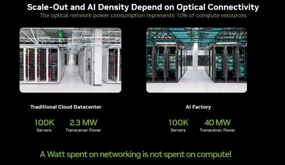
NVIDIA has pointed out that network power consumption in modern AI factories can reach around 40 MW, compared with only 2.3 MW in traditional cloud data centers. Every watt consumed by the network is a watt that cannot be used for computation. As a result, network energy efficiency has become a critical bottleneck limiting the scale of AI factories.

To support AI factories, bothscale-upandscale-outconnectivity challenges must be addressed simultaneously.
Scale-uprefers to high-bandwidth interconnects between multiple GPUs within a rack, forming a massive compute node. The dominant solution today relies on copper cables, but the transmission distance is extremely short.
Scale-out, in contrast, refers to horizontal expansion across racks or even across data centers. This requires long-distance, highly reliable, and high-density optical interconnects.
Therefore, network architectures designed for the AI era must accommodate both scenarios while balancing performance and energy efficiency.
The Core Objective of CPO: Power Efficiency and Reliability

Co-Packaged Optics (CPO) integrates optical transceivers directly alongside the switch ASIC or GPU within the same package. This reduces the long electrical signal paths between the ASIC and external optical modules.
According to NVIDIA’s technical blog, in traditional pluggable optical modules the electrical signal must pass through the printed circuit board, connectors, and external modules. For 200 Gb/s channels, this can result in electrical losses of up to 22 dB, requiring extensive high-speed SerDes and digital signal processing, which increases both power consumption and potential failure points.
CPO addresses this problem by packaging the optical engine directly with the ASIC, reducing electrical loss to roughly 4 dB, while lowering port power consumption to around 9 W. This represents approximately a 3.5× reduction in power consumption, while also improving reliability and port density.
As a result, power efficiency has become the primary evaluation metric for CPO technology. If interconnect power consumption can be reduced to the sub-pJ/bit level, optical interconnects could surpass copper in both cost and performance. This would allow optical interconnects to extend beyond scale-out networks and move into scale-up environments inside the rack, fundamentally reshaping the architecture of AI factories.

Path 1: Narrow & Fast — Incremental Evolution
The Narrow & Fast approach is currently the mainstream path for the evolution of Co-Packaged Optics (CPO) in the industry. Its core concept is to continue using the existing multi-chip module (MCM) architecture while increasing total bandwidth by raising the per-lane modulation rate or adopting higher-order amplitude/phase modulation formats (such as PAM-4, PAM-8, or coherent modulation).
This path introduces relatively small changes to the existing supply chain and benefits from a higher level of technological maturity.
Core Principles and Implementation
Single wavelength + high-speed modulation
A single-wavelength architecture is used, with per-lane data rates gradually increasing from 100 Gb/s to 200 Gb/s, 400 Gb/s, and beyond. High-speed modulation requires drivers, amplifiers, and receivers capable of supporting very high bandwidth, while also introducing complex forward error correction (FEC) and digital signal processing (DSP).
Reuse of the MCM architecture
Key Bottlenecks
The major challenge of the Narrow & Fast approach is that the entire technical burden falls on electronics.
Diminishing energy-efficiency returns
Higher modulation rates reduce receiver sensitivity. To maintain error tolerance, high-power FEC and DSP must be introduced. As a result, energy per bit does not scale linearly downward and may even exhibit diminishing returns.
Research shows that while chip I/O bandwidth requirements are rising rapidly, the number of package pins remains largely unchanged. This forces higher data rates per pin, significantly increasing power consumption.
High-speed circuit and SerDes burden
High-speed modulation requires CML drivers and high-speed SerDes aggregation interfaces, which increases power consumption and latency, while also complicating clock distribution and thermal management.
Thermal pressure and reliability challenges
High-frequency clocks and strong driver circuits generate significant heat, requiring advanced thermal solutions in packaging. Extremely high data rates also reduce the signal-to-noise ratio (SNR) and increase bit-error rates (BER), negatively affecting system reliability.

3月4日
Supply Chain Requirements
The Narrow & Fast path relies heavily on improvements in high-speed modulators and driver technologies. Examples include thin-film lithium tantalate (TFLT) or thin-film lithium niobate (TFLN) Mach–Zehnder modulators and other advanced devices.
Because the overall architecture remains unchanged, the supply chain can largely continue using existing MCM-based solutions, resulting in relatively low adoption barriers.
Narrow & Fast is the most practical short-term solution and can support one to two generations of product iteration. However, its performance ceiling is fundamentally constrained by electronic limitations. As data rates continue to increase, energy-efficiency improvements begin to plateau, making it difficult to meet the increasingly stringent energy-efficiency requirements of AI factories in the long run.

Path 2: Wide & Slow — A Paradigm Shift
The Wide & Slow approach is being actively explored by NVIDIA’s research teams. Its fundamental idea is to introduce multi-wavelength and multi-channel parallel transmission, lowering the data rate per channel (for example, returning to mature 32G NRZ modulation) while increasing total bandwidth through parallelism.
In essence, this approach shifts the technical burden from electronics to photonics.
Core Principles
Multi-wavelength + multi-channel parallelism
In photonics, multiple physical dimensions can be used to increase bandwidth, including time, amplitude/phase, polarization, space, and wavelength.
Research suggests that:
Increasing baud rate (time domain)
Increasing modulation order (amplitude/phase domain)
both lead to rapid increases in power consumption.
By contrast, wavelength-domain scaling faces fewer physical limitations.
Therefore, the Wide & Slow approach advocates:
Dense wavelength-division multiplexing (DWDM) in the wavelength domain
Multi-channel spatial parallelism
This allows per-channel data rates to remain within 25–50 Gb/s, while total bandwidth scales through the multiplication of channel count × wavelength count.
Lower data rate, higher sensitivity
Using mature NRZ (PAM-2) modulation keeps per-channel speeds relatively low. Receiver sensitivity improves, eliminating the need for power-hungry FEC and DSP, and enabling low-power CMOS drivers.
Architectural Implementation
The Wide & Slow approach requires a fundamental change in packaging architecture, typically using a 2.5D silicon interposer that integrates photonic and electronic components on the same silicon layer.
In NVIDIA’s paper “Beyond CPO”, researchers note that interconnect bandwidth exceeding 100 Tb/s will require:
Higher linear density (multi-Tb/s per mm)
Energy efficiency of 1–2 pJ/bit
Such performance can only be achieved by placing optical engines directly on a silicon interposer, where dense routing allows lower per-lane speeds and significantly higher energy efficiency.
Experimental work has demonstrated 50 Gb/s transmission across a 1.2 mm silicon channel in 5 nm CMOS, consuming only 0.3 pJ/bit, highlighting the potential of high-density on-interposer interfaces.

3月10日
Typical Wide & Slow Architectures
Microring modulator/receiver arrays
Microring resonators can function as modulators and filters, enabling multi-wavelength modulation and demodulation in a very small footprint with low power consumption. This architecture is well suited for DWDM systems and avoids complex beam splitters or interferometers, significantly reducing chip area.
Remote light sources and optical frequency combs
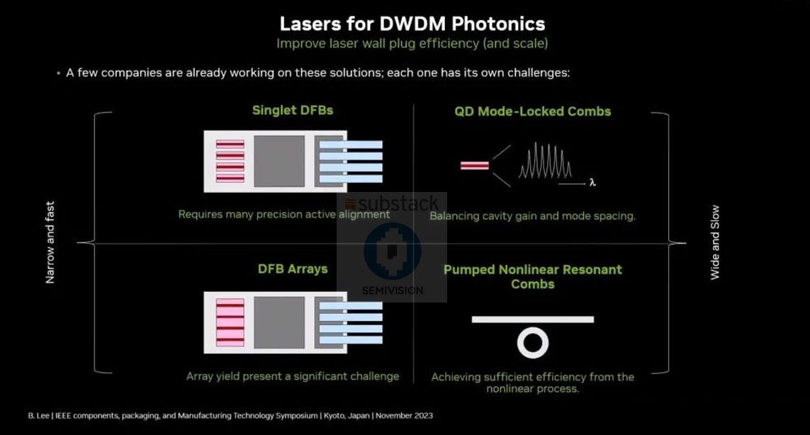
To generate dense wavelength channels, a stable frequency comb light source is required. Research proposes remote mode-locked lasers or optical comb sources, which move heat generation and power consumption outside the module. However, these solutions are still in the early stages of commercialization.
Advantages
The Wide & Slow approach offers several major advantages:
Significantly lower end-to-end energy consumption
Low-speed NRZ modulation improves receiver sensitivity and eliminates FEC/DSP overhead. CMOS drivers reduce circuit power consumption. Electrical interfaces can use simplified or SerDes-free architectures, eliminating clock-recovery jitter and power overhead. Low-frequency clock distribution also consumes far less power.
Reduced thermal pressure
Without high-frequency electrical circuits, thermal load is significantly reduced, making high-density CPO packaging more feasible.
Large optimization potential
Once the power burden shifts to photonics, many optimization opportunities remain. Examples include:
Avalanche photodiodes (APDs) for higher receiver gain
Introducing gain materials
Improved process control to reduce thermal tuning power
The long-term goal is to reduce interconnect energy consumption to below 1 pJ/bit.
Application scope expansion
Once energy consumption reaches sub-pJ/bit, optical interconnects will outperform copper in both cost and performance. This would allow optical links to extend from scale-out networks into intra-rack scale-up environments, eventually covering the entire data-center interconnect stack.

3月6日
Technical Bottlenecks
Despite its promise, the Wide & Slow approach still faces two major challenges:
Advanced packaging and manufacturing
2.5D silicon interposers require mature photonics integration processes, which must be supported by foundries such as TSMC or GlobalFoundries. High-density routing and fiber coupling also require entirely new design methodologies and industry standards.
Light source technology
Multi-wavelength architectures require high-stability optical frequency combs or mode-locked lasers. These devices are not yet fully commercialized, and improvements in cost and reliability are still needed.
2.5D Optics and the Path to Sub-pJ/bit Interconnects
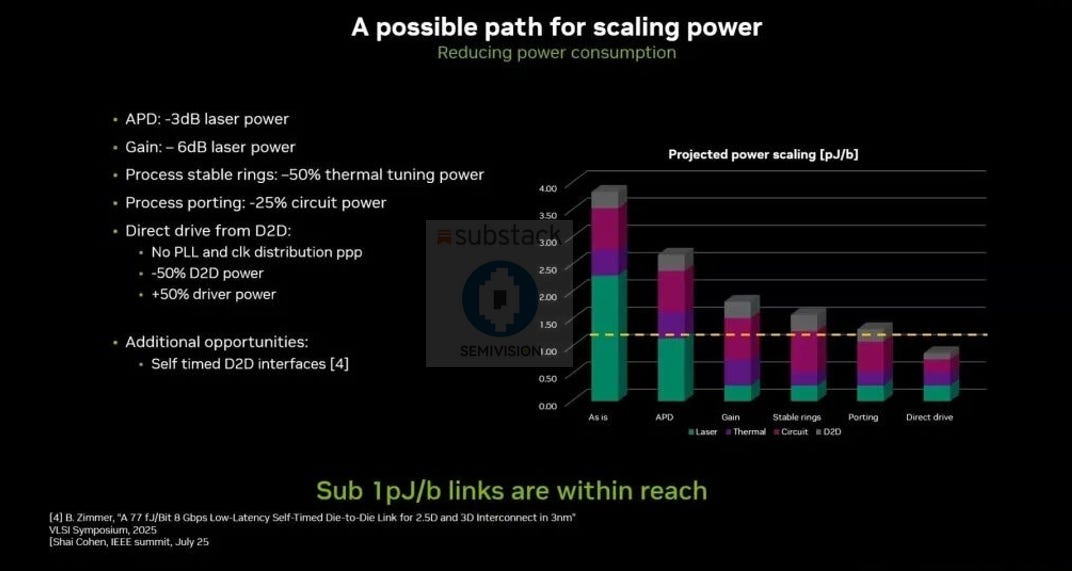
In their presentation, NVIDIA’s research team outlined a pathway toward sub-pJ/bit optical links. By adopting 2.5D optical integration and progressively reducing each component of power consumption, the energy per bit can potentially be reduced from tens of pJ today to around 1 pJ.

2月26日
Power Breakdown and Optimization Strategy
The power consumption of modern CPO modules can generally be divided into four main components:
Laser power consumption (Laser)
Thermal tuning power (Thermal)
Circuit power (Circuit)
Chip-to-chip electrical interface power (Die-to-Die, D2D)
The presentation proposed the following optimization roadmap to progressively reduce the total energy consumption of optical interconnects.
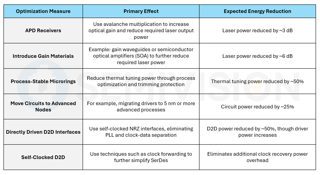
Through these incremental measures, component-level energy consumption can be reduced from more than ten pJ/bit to the sub-pJ/bit level, laying the foundation for wide-and-slow optical architectures.
Example of a 2.5D Optical Architecture
The presentation demonstrated a microring bus architecture implemented on a silicon interposer. In this design, multiple microring modulators are cascaded along a waveguide, with each modulator corresponding to a specific wavelength channel. Multi-channel transmission is achieved through dense wavelength-division multiplexing (DWDM).
At the receiver side, passive microring filters separate the different wavelengths and route them to the corresponding photodetectors for processing.
Under low-speed NRZ/PAM-2 operation at 25–50 Gb/s, this architecture can achieve bandwidth densities of 2–10 Tb/s per mm, while reducing energy consumption to 0.2–0.4 pJ/bit. These results highlight the enormous potential of the wide-and-slow optical architecture.
Common End-to-End Challenges and Supply Chain Coordination
Regardless of whether the narrow-and-fast or wide-and-slow approach is adopted, the large-scale deployment of CPO requires coordination across the entire industry ecosystem.
Thermal management and wavelength stability
High-density CPO packaging operating in non-cooled environments must carefully control heat generation and wavelength drift. This requires technologies such as micro-scale heat dissipation structures and closed-loop thermal tuning control.
Standardized design and testing
Standardized processes must be established across the full stack—from device design and packaging manufacturing to system-level testing—bridging the gap between the photonics and semiconductor industries.
Supply chain collaboration
Key components such as high-speed modulators, optical frequency combs, and silicon interposers require close collaboration among equipment vendors, foundries, device manufacturers, and system integrators in order to enable reliable high-volume production.

2月26日
Outlook and Conclusion
In AI factories, network energy efficiency has become a key bottleneck limiting computational scale. Co-Packaged Optics (CPO) significantly reduces electrical loss and power consumption by placing optical transceivers directly next to the ASIC. However, the long-term direction of CPO depends heavily on architectural choices.
In the short term, the narrow-and-fast approach can leverage mature technologies to iterate rapidly, but its energy-efficiency improvements are limited. Over the long run, electronic speed limitations and thermal constraints are likely to push the industry toward wide-and-slow architectures.
Academic research suggests that reducing per-lane speed while increasing parallelism is a key strategy for improving energy efficiency. The 2.5D silicon interposer architecture provides the density and energy advantages required for this transition, with demonstrations already achieving 50 Gb/s transmission at 0.3 pJ/bit.
The industry has already begun moving in this direction. NVIDIA’s Quantum-X and Spectrum-X Photonics CPO switches, expected to enter commercial deployment in 2026, will deliver 409.6 Tb/s of bandwidth with 512 × 800 Gb/s ports, improving energy efficiency by 3.5× and reliability by 10×.
Once optical link energy consumption drops to the sub-pJ/bit level, optical interconnects will not only address scale-out bottlenecks, but will also penetrate scale-up environments within racks, enabling end-to-end optical connectivity across the entire data center.
Overall, the evolution of CPO technology is not a binary choice between two architectures. Hybrid solutions may emerge—for example, moderate-speed PAM-4 systems with 4 or 8 wavelengths—allowing a smoother transition between approaches.
Regardless of the chosen path, power consumption remains the first principle, and the innovation space in photonics will ultimately determine the future of AI networking infrastructure.
Thanks for reading SEMIVISION @_@! This post is public so feel free to share it.

3月13日


PreviousNext
TopLatestDiscussions








See all