OFC Preview: The Race to 400G per Lane: EML, Silicon Photonics, and TFLN Compete
OFC Preview: The Race to 400G per Lane: EML, Silicon Photonics, and TFLN Compete
- Source: SemiVision
- Author: SEMIVISION
- Published: 2026-03-16T09:35:56+08:00
- URL: https://tspasemiconductor.substack.com/p/ofc-preview-the-race-to-400g-per (1) OFC Preview: The Race to 400G per Lane: EML, Silicon Photonics, and TFLN Compete


OFC Preview: The Race to 400G per Lane: EML, Silicon Photonics, and TFLN Compete
Original Article By SemiVision Research [Reading time: 20 mins]

Mar 16, 2026
∙ Paid
400 G/Lane: A Critical Inflection Point for AI Data Center Interconnects
In recent years, the rapid expansion of generative AI models has driven a dramatic increase in the speed requirements of data center interconnects. Large-scale AI training clusters have evolved from systems with a few hundred GPUs to massive clusters containing tens of thousands of GPUs, making network bandwidth and interconnect efficiency one of the most critical bottlenecks in AI system architecture.

As transmission rates approach hundreds of gigabits per second, traditional copper interconnects begin to suffer from severe signal attenuation and excessive power consumption. In practice, electrical signals transmitted through copper cables are typically limited to distances of less than one meter at such speeds. To support high-throughput communication between remote servers, optical interconnects are rapidly replacing electrical links, becoming a foundational technology for future AI data center infrastructure.
At the 2025–2026 OFC (Optical Fiber Communication Conference), the industry widely recognizes 400 Gb/s per lane optical transmission as the next major milestone for data center interconnects. NVIDIA’s NVLink 6 protocol defines peak SerDes data rates of 400 Gb/s per lane, enabling up to 3.6 Tb/s of bandwidth per GPU. This shift means that both chip-level scale-up interconnects and rack-scale or cluster-level scale-out networks must evolve from 100 G/lane or 200 G/lane architectures to 400 G/lane and beyond.

2025年4月18日

2025年4月8日
According to Taiwan industry report, as electrical signaling losses increase at higher frequencies, optical transmission gains a major advantage through wavelength-division multiplexing (WDM), which allows multiple wavelengths to be transmitted over a single fiber, dramatically increasing data density. As AI clusters continue to grow in scale, major cloud service providers (CSPs) are actively investing in co-packaged optics (CPO) technologies. Industry projections suggest that CPO could reach a penetration rate of around 35% in AI data centers by 2030.
Demonstrations at OFC 2025 by Marvell further confirmed the feasibility of the 400 G/lane architecture. In one experiment, the company achieved 400 Gb/s per lane transmission using 224 GBaud PAM4 modulation, effectively doubling the bandwidth of existing 200 G systems. Analysts note that such breakthroughs require overcoming challenges related to noise, jitter, and attenuation at the electro-optical interface, but once mature, the technology could support 3.2 Tb/s optical links and future switch architectures exceeding 204.8 Tb/s.
Meanwhile, NVIDIA recently announced a $4 billion investment in photonics component suppliers Lumentum and Coherent, ensuring long-term supply of next-generation lasers and modulators. This move highlights how major chipmakers increasingly view optical interconnects as a strategic cornerstone of future data center infrastructure.
Below we will share:
Silicon Photonics Platforms: The Core Path for High-Speed Optoelectronic Integration
New Breakthroughs in High-Speed Silicon Photonic Devices: Global and Chinese Research Progress
Microring Modulators: A Key Device for High-Density Silicon Photonic Interconnects
Thin-Film Lithium Niobate (TFLN): A Potential Mainstream Technology for Ultra-High-Speed Optical Modulators
III–V EML: The Continued Evolution of a Mature Optical Communication Technology
Emerging Materials and New Physical Mechanisms: Exploring the Next Generation of Optical Modulation Platforms
The Industry Significance of the 400 G/Lane Technology Wave

2025年4月3日
POLL
Will you be attending OFC 2026?
Yes
53%
48%
40 VOTES ·
Silicon Photonics Platforms: The Core Path for High-Speed Optoelectronic Integration
Silicon photonics platforms leverage mature CMOS manufacturing processes to fabricate photonic devices and electronic circuits on the same wafer, offering advantages in cost efficiency, scalability, and high-density optoelectronic integration.
According to research from LightCounting, more than 50% of optical transceiver modules are expected to adopt silicon photonics modulators by 2026, compared with only 33% in 2024.
The speed limitations of silicon photonic modulators stem from the relatively weak plasma dispersion effect in silicon, which makes it difficult to simultaneously achieve high modulation efficiency and large bandwidth. To address this challenge, researchers have developed several new architectures:
Slow-light silicon modulators:
By leveraging AI-optimized slow-light structures, researchers have demonstrated 400 Gb/s PAM4 transmission per channel on an eight-channel WDM microring modulator, achieving a chip bandwidth density of 1.6 Tb/s/mm². The design is also thermally insensitive, significantly reducing the need for active temperature control.
Silicon–germanium (SiGe) electro-absorption modulators:
The IHP silicon photonics platform has demonstrated electro-absorption modulators with a 140 GHz cutoff frequency and photodiodes operating at 200 GHz, surpassing the bandwidth limitations of traditional silicon photonic Mach–Zehnder or microring modulators and paving the way for communication speeds exceeding 200 GBaud. Studies show that introducing an appropriate silicon fraction into germanium and using silicon delta-layer epitaxy can shift the absorption edge into the C-band, while maintaining high bandwidth and responsivity.
Hybrid materials and new device architectures:
Research published in Nature Communications (2025) introduced AI-assisted slow-light engineering, where neural networks are used to design slow-light structures capable of achieving 400 Gb/s PAM4 transmission on a pure silicon platform. In addition, NVIDIA and TSMC have collaborated on COUPE 3D packaging technology, stacking 200G PAM4 microring modulators with logic circuits, which significantly increases optical engine bandwidth density while reducing power consumption.
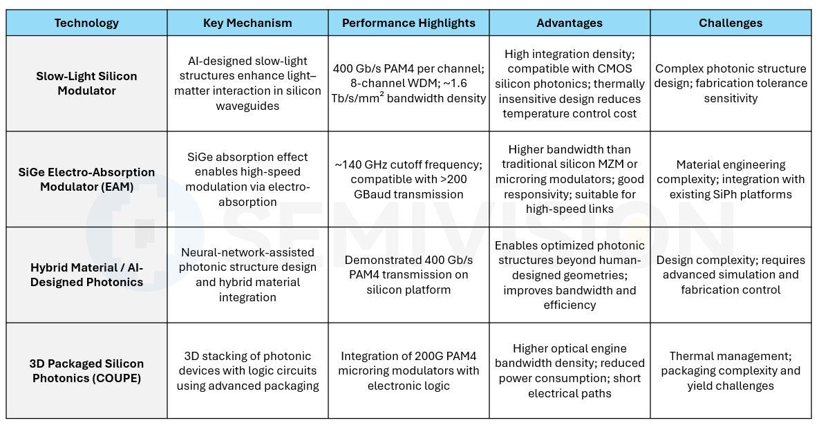
These developments indicate that silicon photonics is evolving from individual device optimization toward system-level co-design. In future data centers, silicon photonics platforms will work in close integration with DSP architectures and advanced packaging technologies, enabling high-bandwidth, low-power, and high-density optoelectronic interconnects.
New Breakthroughs in High-Speed Silicon Photonic Devices: Global and Chinese Research Progress
High-speed optical interconnects impose stringent requirements on optoelectronic components, including bandwidth, extinction ratio, insertion loss, and drive voltage. In recent years, multiple research teams worldwide have achieved significant advances in silicon photonic devices:
Compact Mach–Zehnder Modulators (MZM):
Traditional silicon photonic MZMs are relatively long and have limited modulation efficiency, which restricts system-level integration density. Recent research has demonstrated compact MZMs fabricated on 300 mm CMOS platforms, with device lengths of only a few hundred micrometers and electro-optic bandwidths reaching 94 GHz, enabling 400 Gb/s single-lane transmission. These compact designs significantly reduce chip area and provide a foundation for high-density co-packaged optics (CPO) modules.
Hybrid-Integrated Optical Transmitters:
By bonding silicon photonic traveling-wave MZMs with SiGe BiCMOS drivers, integrated optical transmitters capable of 224 GBaud or higher symbol rates have been demonstrated. A representative example is the 400 G/lane solution presented by Marvell at OFC 2025, which utilizes a complete electro-optical link architecture and achieves 400 Gb/s transmission using 224 GBaud PAM4 modulation. This approach not only doubles the achievable data rate compared with existing systems but also lays the foundation for 3.2 Tb/s optical modules.
High-Bandwidth Electro-Absorption Modulators:
The SiGe photonics platform developed by IHP has demonstrated electro-absorption modulators with a 140 GHz cutoff frequency. These devices feature compact size and low drive voltage, making them well suited for dense photonic arrays. Moreover, the SiGe platform enables the co-fabrication of modulators and high-bandwidth photodetectors within the same process, providing a manufacturable pathway toward transmission speeds exceeding 200 GBaud.
Silicon–Lithium Niobate and Silicon–Organic Hybrid Modulators:
Some research efforts are exploring heterogeneous integration of thin-film lithium niobate (TFLN) or organic electro-optic materials with silicon photonic waveguides. By leveraging the strong Pockels effect, these hybrid modulators can achieve lower VπL, higher bandwidth, and shorter device lengths, while maintaining compatibility with CMOS manufacturing processes.
Chinese research institutions—including Zhangjiang Laboratory, Fudan University, and the Chinese Academy of Sciences…etc — have also invested heavily in silicon photonics research, advancing the field in parallel with global efforts. Because some studies have not yet released detailed public data, this article primarily references international literature and industry reports to present the global development landscape of silicon photonics. As more publications and commercial products emerge, the contributions of Chinese research teams in high-speed silicon photonic technologies are expected to become increasingly visible.
At major international forums such as IEEE ECTC, OFC, and OCP, the number of academic papers from China in areas such as semiconductors, silicon photonics, and quantum technologies currently ranks among the highest. This reflects the country’s large pool of research talent and strong participation in global scientific collaboration. China’s substantial population of engineers and scientists provides a broad foundation for technological research, making it highly competitive in advancing new technologies and contributing to the global innovation ecosystem.
Microring Modulators: A Key Device for High-Density Silicon Photonic Interconnects
Microring modulators (MRMs) offer advantages such as compact size, low power consumption, and high integration density, making them a crucial component for achieving high-density optical interconnects on silicon photonics platforms. However, conventional silicon microrings are limited by factors such as free spectral range (FSR) and quality factor (Q-factor), making it difficult to simultaneously achieve high bandwidth and strong temperature stability. In recent years, researchers have proposed several innovative approaches:
AI-Optimized Slow-Light Microrings:
Research published inNature Communicationsdemonstrated the use of AI-designed slow-light structures to achieve 400 Gb/s PAM4 transmission per channel in an eight-channel WDM module. By using artificial intelligence to optimize waveguide structures and coupling coefficients, the microring modulator achieved a data rate density of 1.6 Tb/s/mm², highlighting the potential of silicon photonics platforms.
Silicon–Germanium (SiGe) Hybrid Microrings:
SiGe electro-absorption modulators (EAMs) can be integrated into microring cavities to provide higher modulation depth and bandwidth. Although the IHP SiGe platform currently focuses on straight-waveguide EAM designs, it could potentially be extended to microring architectures to support large-scale modulator arrays.
Silicon–Organic and Silicon–Lithium Niobate Microrings:
By introducing materials with strong Pockels effects, microring modulators can move beyond reliance on silicon’s plasma dispersion effect. Some research groups have demonstrated microring modulators using organic electro-optic materials or thin-film lithium niobate (TFLN), achieving improved modulation efficiency and enhanced temperature stability.
Silicon Plasmonic Microring Modulators:
A study published inNature Photonics(2023) introduced a resonant plasmonic microring modulator that combines organic electro-optic materials with metallic waveguides to form a nanoscale resonant structure. The device achieved an electro-optic bandwidth of 176 GHz and demonstrated 408 Gb/s intensity modulation within a single resonant cavity. Due to the extremely small optical mode volume in plasmonic structures, the device’s temperature sensitivity is reduced by 28×, eliminating the need for complex thermal control systems. This technology is considered a potential alternative to conventional silicon microring modulators and may play a role in 1.6 Tb/s or even higher-speed interconnects.
The success of microring modulators ultimately depends on balancing bandwidth, extinction ratio, insertion loss, and temperature stability. Through AI-assisted structural optimization, the introduction of high-performance electro-optic materials, and precise packaging control, microring modulators are expected to play a central role in future data center optical interconnect architectures.
2025年5月15日
Thin-Film Lithium Niobate (TFLN): A Potential Mainstream Technology for Ultra-High-Speed Optical Modulators
In addition to silicon photonics platforms, thin-film lithium niobate (TFLN) has rapidly emerged in recent years as one of the most promising technologies for high-speed optical modulators. Unlike conventional silicon photonic modulators that rely on the plasma dispersion effect for modulation, TFLN devices utilize the material’s intrinsic electro-optic Pockels effect to achieve phase modulation. This mechanism allows TFLN modulators to maintain very high bandwidth while significantly reducing drive voltage and optical loss. Because lithium niobate exhibits a high electro-optic coefficient and extremely low optical absorption, TFLN modulators show strong potential for both high-speed data center optical interconnects and long-haul optical communication systems.
From a materials perspective, one of the core advantages of TFLN is its extremely fast electro-optic response. Since the Pockels effect is essentially an instantaneous electro-optic mechanism, its response time can reach the femtosecond scale, far faster than silicon modulators that rely on carrier injection or depletion effects, which typically operate at nanosecond timescales. This physical property enables TFLN modulators to support electro-optic bandwidths exceeding 100 GHz, providing the theoretical foundation for high-speed optical transmission beyond 200 GBaud. Multiple studies presented at OFC and ECOC have demonstrated TFLN Mach–Zehnder modulators with electro-optic bandwidths exceeding 110 GHz, achieving experimental single-channel transmission rates above 400 Gb/s using modulation formats such as PAM4, PAM6, and PAM8.
Beyond high bandwidth and rapid response, TFLN also offers significant advantages in power efficiency and optical performance. Because of its high modulation efficiency, TFLN modulators can achieve the required phase shift with lower drive voltages, reducing overall system power consumption in practical data center applications. For example, in 800G-DR8 optical module architectures, optical transmitters using TFLN modulators can reduce power consumption by approximately 20–25% compared with conventional silicon microring modulators. Additionally, TFLN waveguides exhibit extremely low optical propagation loss, typically below 0.04 dB/cm in the C-band, significantly lower than many silicon photonic waveguides. This low-loss characteristic is particularly valuable for long-distance data center interconnects and high-density WDM systems.
From a spectral standpoint, TFLN also provides a very wide optical transparency window. Lithium niobate remains transparent across wavelengths ranging from 400 nm to 5 μm, covering visible, near-infrared, and mid-infrared regions. This property allows the TFLN platform to support not only traditional C-band and O-band optical communications, but also emerging applications such as optical computing, photonic sensing, and mid-infrared photonics. Thanks to its low absorption and low dispersion characteristics, TFLN also demonstrates strong stability in high-power optical transmission environments.
At the system architecture level, TFLN modulators can also simplify optical transceiver design. In certain next-generation data center optical module architectures, an eight-channel optical transceiver can operate using a single continuous-wave (CW) laser source, with high-speed modulators generating multiple channels. This approach can reduce the number of required lasers, fibers, and microlens components by half, thereby lowering packaging complexity and manufacturing cost. As optical module speeds increase toward 1.6T and 3.2T, such highly integrated architectures will become increasingly important.
From a market perspective, TFLN is rapidly becoming a key material platform for high-speed optical interconnects. Driven by the growth of generative AI and hyperscale data centers, the high-speed optical module market is entering a period of rapid expansion. Several market research firms predict that the TFLN photonics device market could achieve a compound annual growth rate (CAGR) exceeding 70% between 2024 and 2030. Industry roadmaps also suggest that TFLN could become one of the core materials for the 3.2 Tb/s optical module generation, particularly in architectures such as LPO (Linear Pluggable Optics), LRO (Linear Receive Optics), and coherent optical modules, where TFLN modulators can provide higher bandwidth and lower power consumption. Many forecasts indicate that 3.2T pluggable optical modules may enter large-scale commercial deployment around 2027–2028.

2025年6月16日
Despite its promising outlook, however, the industrialization of TFLN still faces several technical challenges. The first relates to materials processing and integration with silicon photonics. Because TFLN devices often require heterogeneous integration with silicon platforms, the high-temperature thermal oxidation processes used in silicon wafer fabrication can lead to lithium diffusion, potentially causing contamination that affects CMOS process reliability and yield. As a result, additional isolation layers and packaging techniques are required in mass production to prevent material contamination.
A second challenge involves process compatibility. Some TFLN fabrication techniques still rely on non-CMOS-compatible materials and processes, such as gold electrodes or electron-beam lithography. These requirements make it difficult to directly integrate TFLN manufacturing into existing 12-inch CMOS wafer fabs, increasing the complexity of scaling production. To enable large-scale commercialization, more standardized and CMOS-compatible fabrication processes will need to be developed.
Finally, cost and supply chain issues remain important considerations. TFLN wafers are typically produced using complex processes such as ion implantation, wafer bonding, and layer transfer, which currently result in relatively high costs and limited global production capacity. At present, the TFLN wafer supply chain is concentrated among a small number of materials suppliers, including several emerging companies in China such asAFR, Liobate, and OriChip. As demand grows, establishing a stable and scalable materials supply chain will become a key factor in determining how quickly TFLN technology can reach widespread commercialization.
Overall, thanks to its ultra-high bandwidth capability, extremely low power consumption, and excellent optical properties, thin-film lithium niobate is increasingly recognized as one of the most promising mainstream technologies for high-speed optical modulators. As fabrication processes mature and industry investment accelerates, TFLN is expected to play a critical role in future 400G/lane and even 800G/lane data center optical interconnect systems, alongside silicon photonics and III-V photonic devices, forming a key foundation for next-generation optical communication technologies.

[2026/3/13]HyperLight,UMC, and its wholly owned subsidiary Wavetek announced a collaboration withJabilto accelerate the deployment of thin-film lithium niobate (TFLN) photonic technology for interconnects in hyperscale AI data centers.
This partnership combines HyperLight’s TFLN photonics technology, the proven wafer-foundry manufacturing capabilities of UMC and UOEC, and Jabil’s expertise in mass production manufacturing and assembly, jointly advancing the widespread adoption of next-generation optical modules in data centers.
As AI computing scales rapidly, optical interconnect technologies must increase bandwidth while avoiding becoming a bottleneck in overall system power consumption. HyperLight is working closely with Jabil to integrate TFLN-based photonic devices into next-generation optical transceiver module platforms.
With UMC and UOEC providing scalable 6-inch and 8-inch wafer manufacturing capacity, combined with Jabil’s expertise in supply-chain management and system integration, the collaboration paves the way for HyperLight’s TFLN chiplet platform to enter large-scale market adoption and enable broad deployment of high-performance optical modules.
Mian Zhang, CEO of HyperLight, said:
“TFLN delivers significant advantages for AI data-center networking by reducing power consumption and lowering laser requirements. As optical interconnect speeds continue to increase, the material advantages of TFLN will become even more evident. By combining Jabil’s capabilities in system integration and manufacturing with the scalable device production support from UMC and UOEC, we are moving TFLN from innovation toward real-world deployment, accelerating its adoption in hyperscale data centers.”
Jason Wildt, Senior Vice President and General Manager of Jabil’s Photonics Business Unit, stated:
“Hyperscale and AI customers must deploy their solutions at massive scale, which means the optical technologies they adopt must be capable of reliable high-volume production and integration at the data-center level. Our collaboration with HyperLight, UMC, and UOEC combines advanced photonics technology, mature manufacturing capabilities, and system-integration expertise, enabling TFLN-based solutions to be deployed at the rack level to meet the needs of AI and hyperscale customers.”

Kuei-Chun Hung, Senior Vice President at UMC, added:
“Through our collaboration with HyperLight, UMC has helped move TFLN from early-stage development toward proven foundry manufacturing. Expanding this collaboration with Jabil for system-level integration helps establish a complete manufacturing and deployment pathway to meet the scale, reliability, and capacity requirements of AI data-center infrastructure.”
Compared with current optical modules, HyperLight’s TFLN technology can significantly reduce power consumption, and its advantages are expected to grow further as channel transmission speeds increase. In the target architecture, TFLN enables simplified optical designs, such as reducing the number of required lasers, thereby addressing both power consumption and supply constraints.
At hyperscale deployment levels, improvements at the individual module level accumulate, ultimately improving data-center-level energy efficiency. This enables operators to deploy more GPUs, larger compute clusters, or support a greater number of AI workloads.

3月5日
III–V EML: The Continued Evolution of a Mature Optical Communication Technology
III–V semiconductor materials possess direct bandgaps and high carrier mobility, making them well suited for lasers and electro-absorption modulators (Electro-Absorption Modulated Lasers, EMLs). Traditional EMLs have been widely deployed in 100G and 200G optical modules, and the technology continues to evolve in the 400G/lane era.
At OFC 2025,Coherentdemonstrated the industry’s first 400 Gb/s differential-drive EML (D-EML)(News link). Building upon its earlier 200G D-EML technology, the new design employs a bipolar differential architecture that doubles the signal amplitude, significantly reducing power consumption while improving optical modulation amplitude and extinction ratio. An integrated on-chip termination network further optimizes electrical performance and reduces the preprocessing requirements of the front-end DSP, resulting in a simpler electro-optical link architecture. The company noted that this differential EML technology is intended to provide a cost-effective, high-performance optical source for future 1.6T and 3.2T systems.

3月4日
Another development direction for III–V EML technology involves multi-section device architectures and broadband design. Researchers have demonstrated that cascading two electro-absorption modulators can increase the 3-dB bandwidth while lowering the drive voltage, enabling transmission rates of 360 Gb/s PAM4 or 413 Gb/s PAM6. Unlike silicon photonics platforms, III–V devices integrate the laser source directly on chip, eliminating the need for external lasers and simplifying monolithic integration. In addition, InP-based transmitters can integrate semiconductor optical amplifiers (SOA) and distributed feedback (DFB) lasers, delivering optical output powers above +5 dBm, which is advantageous for long-reach directly modulated transmission.
Although silicon photonics and emerging material platforms are advancing rapidly, III–V EML technology retains several irreplaceable advantages, including mature manufacturing processes, better temperature stability, and lower insertion loss. With the introduction of differential driving architectures and cascaded modulator structures, EMLs are expected to remain relevant in the 400G/lane era, particularly in applications requiring high optical power and large dynamic range.

3月14日
Emerging Materials and New Physical Mechanisms: Exploring the Next Generation of Optical Modulation Platforms
In addition to silicon photonics and lithium niobate platforms, researchers are actively exploring new materials and physical mechanisms to overcome the limitations of current optical modulators. Several representative research directions include:
- Silicon Plasmonic Modulators
A resonant plasmonic microring modulator reported inNature Photonicsuses a metal–insulator–silicon structure combined with organic electro-optic materials, achieving an electro-optic bandwidth of 176 GHz and 408 Gb/s intensity modulation. Due to the extremely small optical mode volume of plasmonic structures, the device’s sensitivity to temperature variation is reduced by 28×. Such architectures could provide compact and low-power solutions for optical interconnects beyond 1.6 Tb/s.
- Ferroelectric Nematic Liquid Crystal (FNLC) Modulators
A 2025 study demonstrated a Mach–Zehnder modulator combining silicon photonics with ferroelectric nematic liquid crystals. The device achieved a Vπ·L product of 0.3 V·cm, enabling 102 Gb/s PAM4 transmission in the C-band under a 3.5 V DC bias. FNLC materials feature high dielectric constants and strong spontaneous polarization, potentially enabling extremely low-voltage modulation, although the technology remains in an early research stage.
- Silicon–Organic Hybrid (SOH) Modulators and High-Performance EO Polymers

Organic electro-optic materials can exhibit electro-optic coefficients exceeding 1000 pm/V. SOH modulators combine the mature fabrication processes of silicon waveguides with the high efficiency of organic materials, enabling low Vπ operation within extremely short modulation arms. Research indicates that SOH modulators can achieve half-wave voltages below 0.5 V and bandwidths exceeding 100 GHz, making them suitable for short-reach high-speed interconnects. However, long-term thermal stability remains a challenge.
2025年6月16日
- Terahertz (THz) Interconnects
According to EE Times, startupAttoTudeunveiled a terahertz RF interconnect platform at OFC 2025. By combining high-capacity ASIC processes with specialized cable design, the company has developed a low-power interconnect technology capable of transmitting terahertz-frequency signals over copper cables, with initial target distances of around 40 meters.
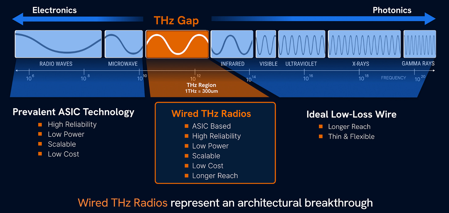
The founders suggest that this architecture could potentially replace short-reach CPO or pluggable optical modules, addressing challenges in power efficiency and reliability within data centers. Some investors believe the technology could enable a new generation of interconnect architectures over the next decade.

Although these new materials and physical mechanisms have not yet reached large-scale commercialization, they provide promising alternatives for future optical modulation technologies. In the long term, high-speed optical interconnects will likely adopt a heterogeneous ecosystem of technologies, combining different platforms to meet diverse requirements in performance, power efficiency, and cost.
The Industry Significance of the 400 G/Lane Technology Wave
The rise of 400 G/lane technology represents not only a step forward in transmission speed but also a fundamental reshaping of the industry structure. From an industry perspective, several trends are likely to emerge over the next few years:
Rapid evolution of optical module speeds:
Once 400 G/lane becomes mature, the industry is expected to quickly move toward 800 G/lane, 1.6 T/lane, and even higher speeds. The 1.6 T silicon photonics engine and 200 G/lane architecture demonstrated by Marvell at OFC 2025 already hint at the early form of 3.2 T optical modules. With the introduction of advanced modulation formats such as PAM4, PAM6, and PAM8, along with improved forward error correction (FEC) technologies, a single optical fiber will be able to carry significantly larger volumes of data.
Co-design of packaging and system architectures:
Technologies such as CPO (Co-Packaged Optics), LPO (Linear Packaged Optics), and CPC (Co-Packaged Copper) will become critical for enabling hundreds-of-terabit switches and massive AI clusters. Chipmakers and optical vendors are increasingly collaborating on 3D integration and optoelectronic packaging technologies, such as TSMC’s COUPE 3D architecture, which integrates 200 G PAM4 microring modulators with advanced packaging structures.
Supply chain restructuring and capital investment:
As the strategic importance and technical complexity of optical interconnects increase, foundries are expanding silicon photonics manufacturing capacity. For example, NVIDIA has invested in suppliers such as Lumentum and Coherent to secure long-term access to critical lasers and modulators. Meanwhile, startups includingAttoTudeandRetymhave attracted significant funding as they pursue breakthroughs in THz interconnect technologies and programmable DSP architectures.


Coexistence of multiple technology pathways:
Future data center optical interconnects will likely adopt a multi-technology ecosystem, combining silicon photonics, thin-film lithium niobate, III–V EML devices, and emerging hybrid materials. Silicon photonics will likely dominate due to its cost advantages and integration capability, while lithium niobate and other advanced materials may provide differentiated solutions for ultra-high-frequency or ultra-low-power applications.
Overall, 400 G/lane is not merely a technical milestone in optical communications but a foundational technology for the next generation of AI computing infrastructure. As data center scale continues to expand, optical interconnect technologies are poised to enter a new decade of rapid growth and innovation.
Emerging Industry Direction
Looking ahead, the industry is moving toward deep integration between compute, photonics, and advanced packaging. Optical I/O will increasingly shift from pluggable modules to chip-level integration, eventually enabling direct optical connectivity within GPUs, switches, and AI accelerators. This convergence of photonics, semiconductors, and system architecture will define the next phase of AI infrastructure development.

2月28日


PreviousNext
TopLatestDiscussions








See all