SemiVision Panel - From CoWoS to Optical I/O : Mapping the Future of AI Interconnects
SemiVision Panel - From CoWoS to Optical I/O : Mapping the Future of AI Interconnects
- Source: SemiVision
- Author: SEMIVISION
- Published: 2026-03-13T14:10:59+08:00
- URL: https://tspasemiconductor.substack.com/p/semivision-panel-from-cowos-to-optical (1) SemiVision Panel - From CoWoS to Optical I/O : Mapping the Future of AI Interconnects


SemiVision Panel - From CoWoS to Optical I/O : Mapping the Future of AI Interconnects
Original Artcle By SemiVision Research [Reading time: 10 mins]

Mar 13, 2026
∙ Paid
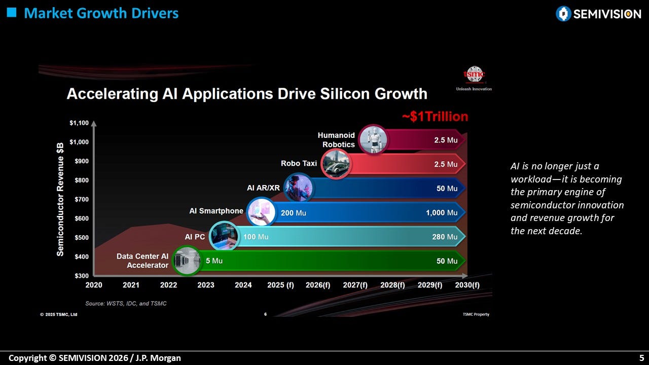
In the new era of AI-centric computing, electrical interconnects alone are no longer sufficient to support the explosive growth in data movement required by ever-larger models. Traditional copper interconnects face severe challenges in power consumption, latency, and routing congestion at high data rates. As a result, the industry is increasingly turning to optical interconnects.
Optical signals can travel through fiber with very low loss, enabling bandwidths of several terabits per second while significantly reducing energy per bit (pJ/bit) and latency (ns). Major semiconductor manufacturers have begun integrating optical engines into advanced packaging platforms to sustain scalability and energy efficiency in the post-Moore computing era.
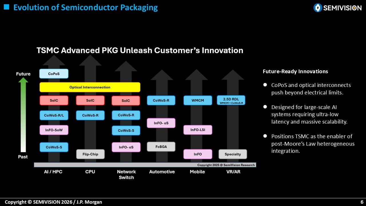
TSMC has indicated in its CoWoS platform roadmap that CoPoS and optical interconnect technologies push innovation beyond the limits of electrical signaling, enabling ultra-low latency and highly scalable architectures for large AI systems.

2026/3/12 Taipei
Based on slides from theSemiVision 2026 / J.P. Morgan report, combined with recent public industry information, this article outlines the evolving optical interconnect technology roadmap, covering packaging architectures, silicon photonics platforms and key components, emerging industry innovators, and the testing and material challenges ahead.



2025年12月31日

Optical Interconnect Demand and Packaging Evolution
Limits of Electrical Interconnects
In conventional packaging architectures, processors and memory exchange data through copper interconnects. As bandwidth demand grows, designers must either increase serial data rates or add more wires.
However, more wires increase package size and power consumption, while higher speeds make jitter, signal loss, and equalization increasingly difficult to manage.
The report notes that TSMC’s CoWoS platform is entering a new phase of heterogeneous integration, combining HBM memory, high-performance GPUs, and optical engines (Optical I/O) within a single package.
Optical engines create high-speed communication channels between chips using short-reach optical fibers, alleviating routing congestion within the package substrate.
CoPoS and NPO: From Co-Packaged Optics to Near-Packaged Optics
TSMC categorizes optical engine products into two main architectures:
Co-Packaged Optics (CPO)andNear-Packaged Optics (NPO).
CPO integrates the optical engine directly with a switching ASIC on the same substrate, achieving the shortest possible interconnect distance and the highest energy efficiency.
NPO, by contrast, implements the optical engine as a pluggable module, improving serviceability while retaining roughly 80% of the energy efficiency of CPO.
Key differences highlighted in the report include:
Configuration
CPO integrates the optical engine directly with the switching ASIC within the same package.
NPO uses pluggable optical modules, allowing failed optical engines to be replaced independently.
Interconnect distance and power
CPO interconnect distance is typically < 5 cm, reducing power consumption by more than 50%.
NPO maintains roughly 80% of the energy efficiency of CPO at short reach.
Maintainability and yield
CPO integrates the entire system on a single board, making repair more difficult and increasing packaging complexity and yield pressure.
NPO’s modular architecture allows faulty optical modules to be replaced individually, reducing packaging complexity and improving manufacturability.
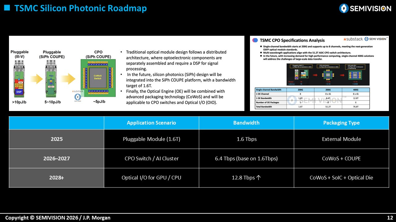
The report also outlines a projected timeline:
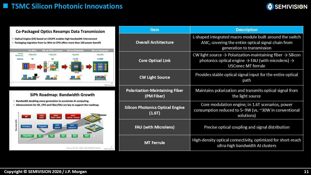
2025:Launch of 1.6 Tb/s pluggable optical modules
2026–2027:Deployment of CPO in AI switches and clusters, integrating CoWoS and COUPE technologies to reach 6.4 Tb/s
Beyond 2028:Optical I/O integrated directly into GPU/CPU packages, enabling bandwidths of 12.8 Tb/s

3月13日

TSMC Silicon Photonics Platform and Optical Engines
Heterogeneous Integration and Packaging Innovation
Silicon photonics technology lies at the core of optical interconnect development.
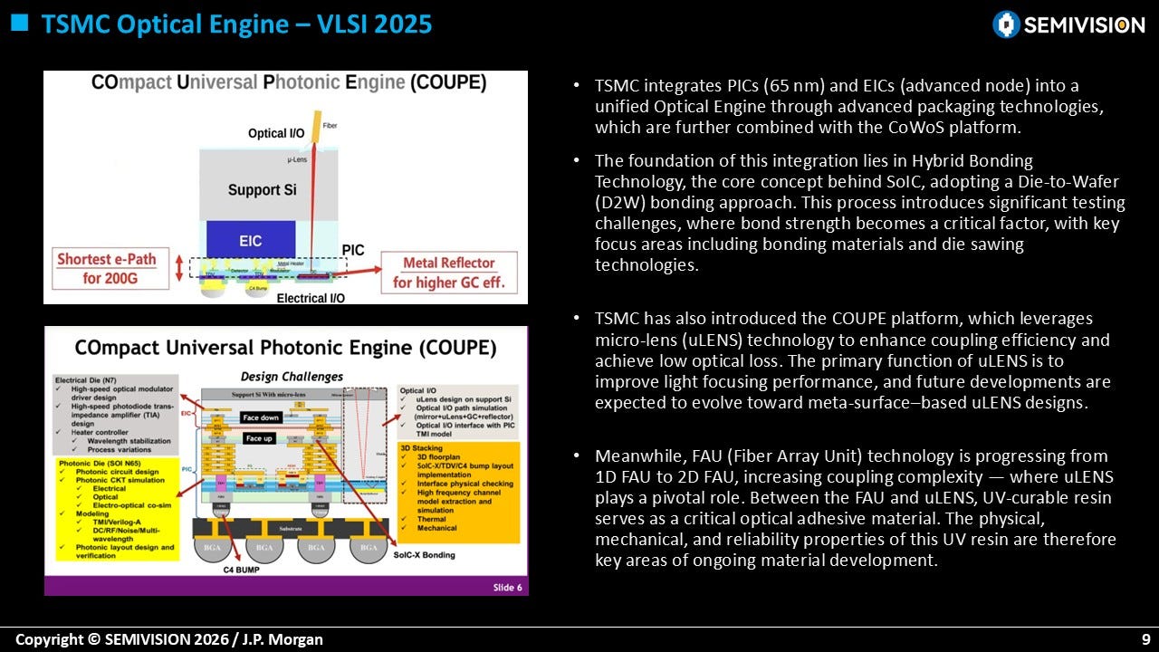
TSMC integrates 65 nm photonic integrated circuits (PIC) with advanced-node electronic integrated circuits (EIC) to form a unified optical engine architecture.
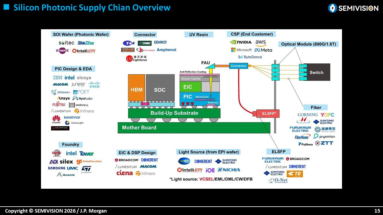
This integration uses SoIC hybrid bonding, enabling die-to-wafer (D2W) packaging with extremely high precision.
The COUPE platform further enhances optical coupling efficiency through the use of micro-lenses (uLENS), with future development targeting metasurface lenses.
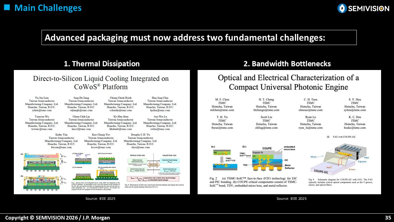
The report notes that fiber array units (FAUs) are evolving from 1D to 2D structures, and when combined with micro-lens arrays can effectively control optical coupling loss.
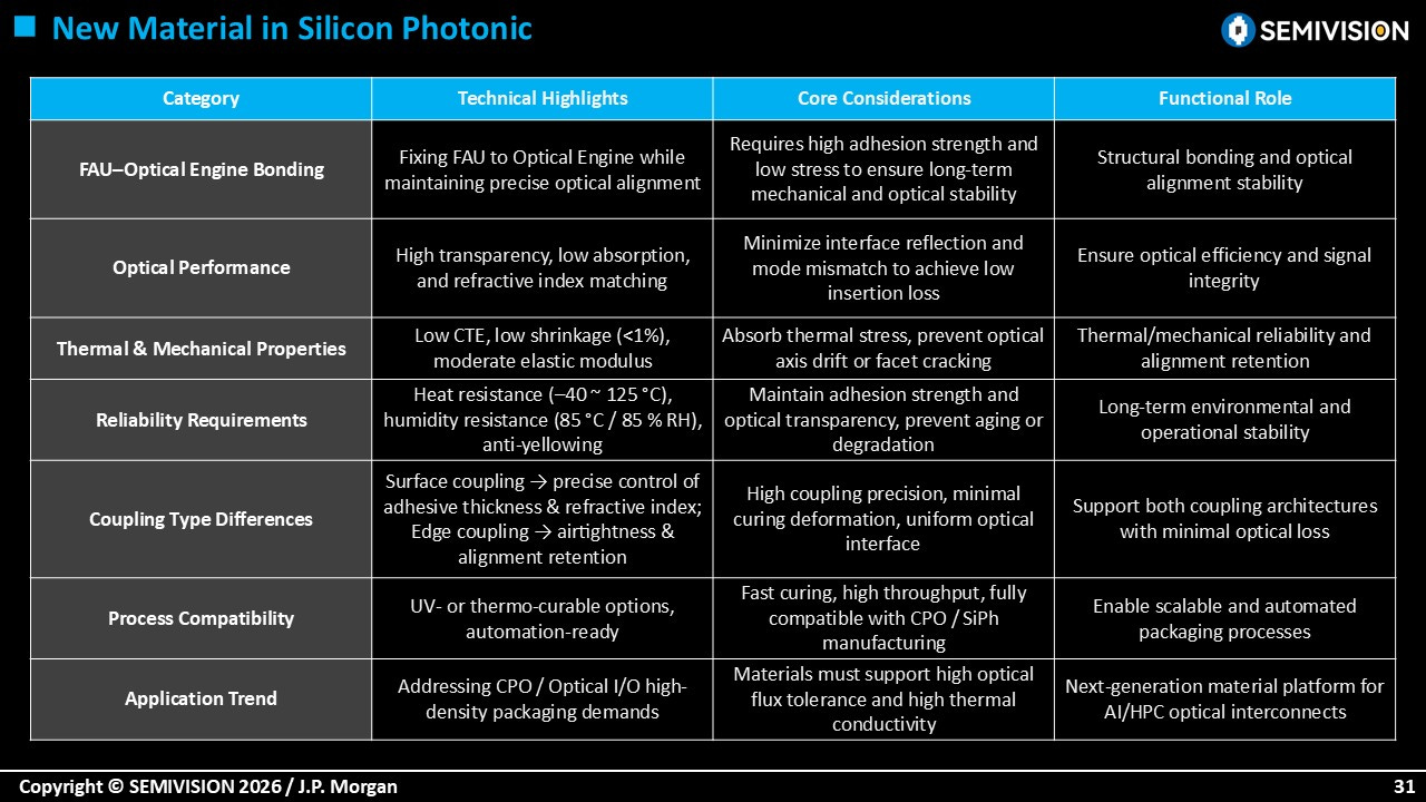
Meanwhile, UV-curable resins play a crucial role as optical bonding materials, as their optical and mechanical properties directly affect coupling efficiency and long-term reliability.

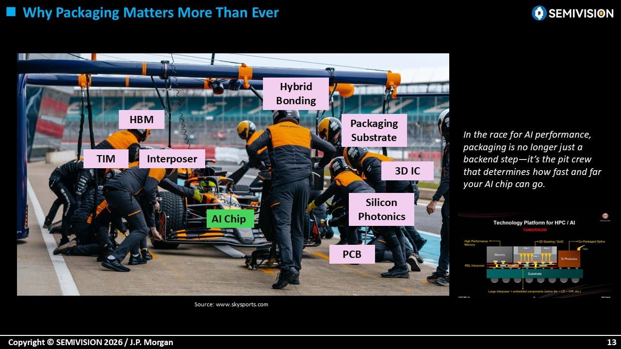
Advanced Packaging and Thermal Engineering
On the packaging side, TSMC combines SoIC-X and COUPE technologies to achieve optical alignment precision of ±0.5 µm.
Graphite heat spreaders
Thermal interface materials (TIM)
Thermoelectric modules
These cross-layer technologies help suppress heat accumulation under high power densities.
Together, they enable the integration of lasers, modulators, and photodetectors within a single chip, creating a truly monolithic optoelectronic system.

Optical Engine Architecture
The optical engine into multiple functional components.

Through these building blocks, TSMC can assemble an L-shaped integrated mega-module that covers the entire optical link—from light generation to signal transmission. In 1.6 Tb/s applications, the optical engine consumes only 5–9 W, representing a substantial reduction compared with traditional ~30 W solutions.
Timeline and Application Scenarios
TSMC’s silicon photonics roadmap divides optical engine deployment into three stages:
2025 – Pluggable Modules (1.6 Tb/s)
External pluggable modules used in switches and early AI systems, providing 1.6 Tb/s bandwidth and classified as Near-Packaged Optics (NPO).
2026–2027 – CPO Switches / AI Clusters (6.4 Tb/s)
Optical engines co-packaged with switching ASICs using CoWoS + COUPE, delivering 6.4 Tb/s bandwidth (based on a 1.6T optical engine).
Beyond 2028 – Optical I/O for GPU/CPU (≥ 12.8 Tb/s)
Optical engines integrated directly into GPU/CPU packages, leveraging 3D packaging technologies such as CoWoS, SoIC, and optical chiplets to enable interconnect bandwidth exceeding 12.8 Tb/s.


Testing and Mass Production Challenges
Testing for optical interconnect technologies still lacks a fully standardized process across the industry. The report notes that in highly automated, high-volume testing environments, optical probing technologies have yet to reach mature standardization. At present, most testing setups rely on multi-axis active alignment or passive alignment techniques to connect optical fibers with photonic devices.
Handling of fiber connections and calibration of optical measurement instruments also remains largely non-standardized. In many cases, testing workflows depend on customized setups and manual intervention, which limits scalability and throughput.
2025年7月16日
To achieve true high-volume manufacturing, several key capabilities must be developed and integrated:
Optical probes, fiber sockets, and optical test instrumentation must be deeply integrated with existing electrical test platforms.
Testing infrastructure must support automation, high throughput, and high-density parallel testing comparable to modern semiconductor wafer-level test systems.
Advanced alignment technologies are required to maintain sub-micron optical coupling precision during automated testing.
New testing methodologies must support both wafer-level and package-level validation of photonic devices.
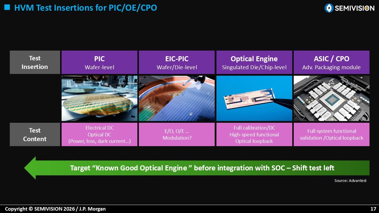
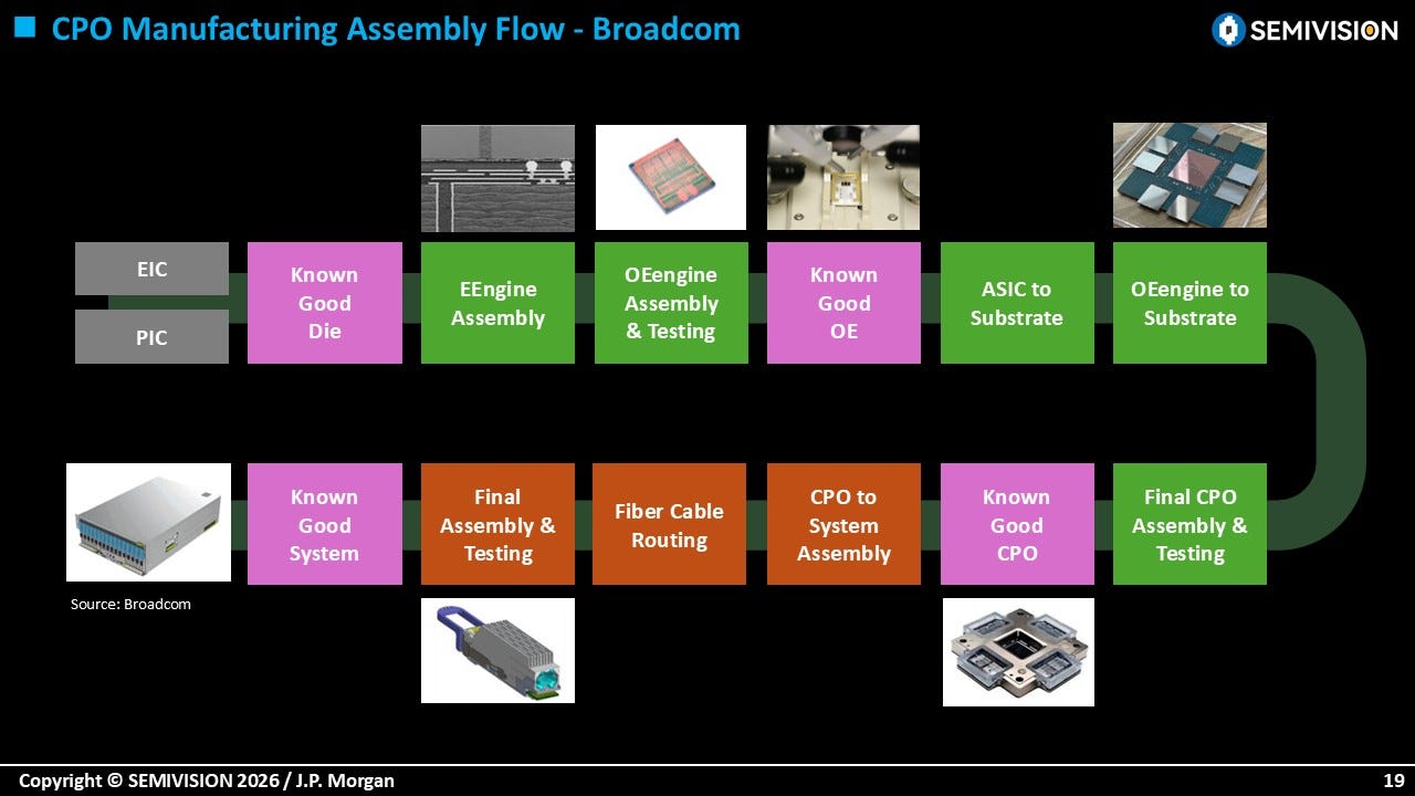
Another critical requirement is the development of a known-good optical engine (KGOE) testing flow. Similar to the concept of known-good dies (KGD) in advanced packaging, optical engines must be fully validated for functionality, performance, and reliability before they are integrated with system-on-chip (SoC) devices.
Without such pre-integration validation, defective optical components could compromise the yield of highly complex heterogeneous packages such as CoWoS, SoIC, and other 3D-integrated systems.

2025年8月10日
As optical engines become tightly integrated with GPUs, CPUs, and AI accelerators, testing strategies will need to evolve toward co-optimized electro-optical test frameworks, combining semiconductor testing methodologies with precision optical measurement techniques. Achieving this level of integration is essential for enabling the scalable mass production of optical I/O systems for next-generation AI infrastructure.

3D Silicon Photonics and NVIDIA’s Breakthrough
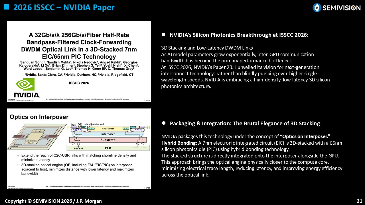
At the 2026 International Solid-State Circuits Conference (ISSCC), NVIDIA presented a paper titled “Optics on Interposer,” demonstrating an innovative architecture that stacks silicon photonic chips with electronic ICs using 3D integration. The key concepts include:
3D Stacking and Hybrid Bonding:
A 7 nm electronic integrated circuit is stacked with a 65 nm silicon photonics die using hybrid bonding and directly integrated onto the interposer next to the GPU. This approach shortens the distance between the optical engine and the compute core, reducing electrical routing complexity and latency.
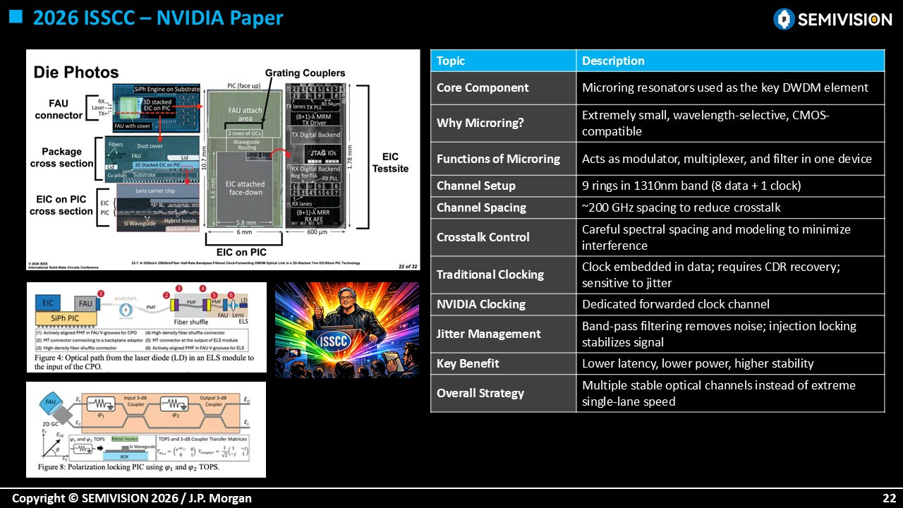
DWDM Micro-Ring Resonators:
Micro-ring resonators are used as modulators, multiplexers, and filters. In the 1310 nm wavelength band, nine rings are configured—eight for data channels and one for the clock. Each channel is spaced at approximately 200 GHz, helping reduce crosstalk.
Dedicated Forward Clock and Jitter Management:
Unlike conventional approaches that embed the clock within the data stream, NVIDIA proposes a dedicated forward clock channel. Signal stability is achieved through band-pass filtering and injection-locking techniques, enabling lower latency and improved power efficiency.
Multi-Channel Strategy:
Instead of pushing extremely high speeds on a single optical channel, NVIDIA emphasizes using multiple stable optical channels, which helps control power consumption and reduces manufacturing complexity.

2月26日

2月28日
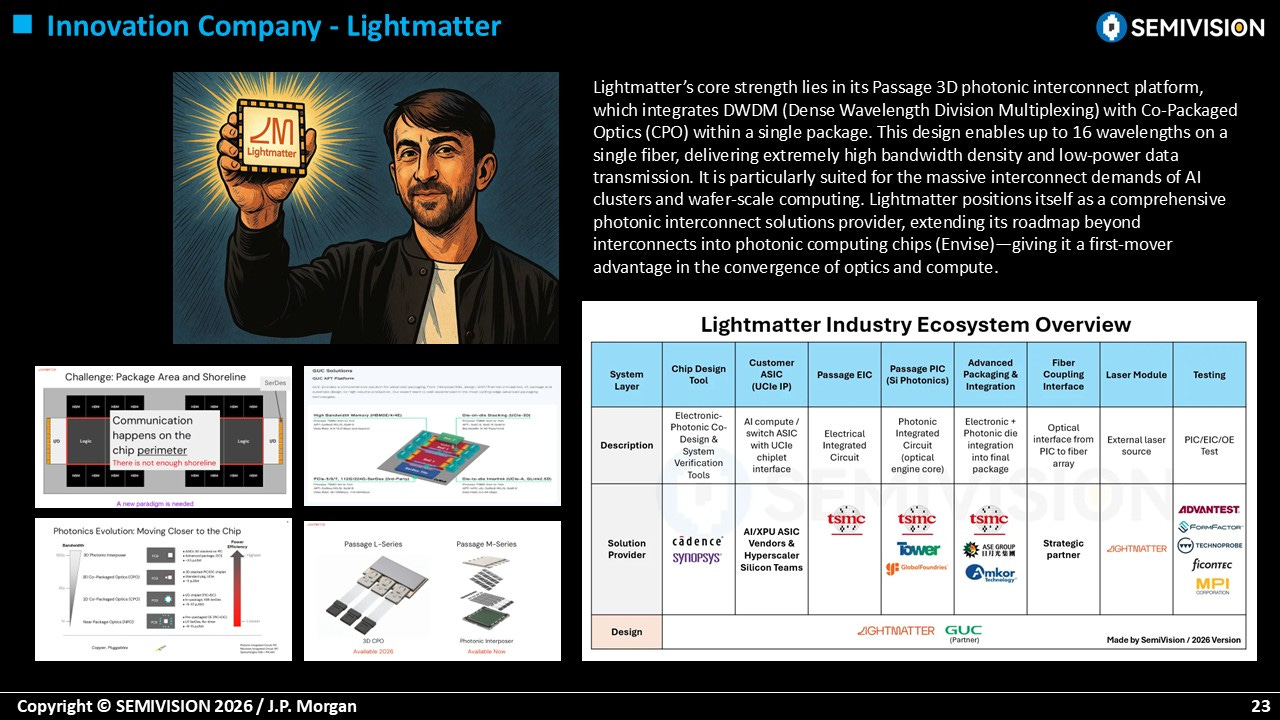
Lightmatter – Passage 3D Platform
Lightmatter positions its core advantage in the Passage 3D optical interconnect platform. This platform integrates dense wavelength division multiplexing (DWDM) with co-packaged optics (CPO) within a single package. A single optical fiber can carry up to 16 wavelengths, delivering extremely high bandwidth density and low-power data transmission.

1月29日
This architecture is particularly well suited for the massive interconnect requirements of AI clusters and wafer-scale computing systems. Lightmatter also notes that its technology roadmap extends toward optical computing chips (Envise), combining computation and interconnect capabilities, which gives the company a first-mover advantage in the emerging field of optoelectronic integration.

Celestial AI / Marvell – Photonic Fabric Platform
Celestial AI (now part of Marvell) demonstrated its Photonic Fabric platform at OFC 2024. The platform is an optical interconnect solution designed to support chip-to-chip communication and compute-to-memory connectivity.
It utilizes germanium-silicon (GeSi) electro-absorption modulators (EAM). Compared with the Mach–Zehnder modulators (MZM) or micro-ring modulators commonly used in mainstream silicon photonics, this approach exhibits distinct characteristics.

2025年7月4日
Celestial AI emphasizes that its GeSi EAM avoids the thermal tuning limitations associated with Mach–Zehnder modulators (MZM) and micro-ring modulators (MRM), enabling more stable optical interconnect performance across varying temperature conditions.
The Photonic Fabric platform also supports multimode operation, providing advantages for chip-to-memory interconnects.

Ayar Labs – Optical I/O and the TeraPHY Engine
Ayar Labs focuses on integrating optical I/O directly into advanced packaging and ASIC architectures, enabling AI accelerators to scale through system-level optical connectivity. Its flagship product, the TeraPHY optical I/O engine, uses co-packaged optics (CPO) technology to replace traditional copper interconnects that suffer from high power consumption and bandwidth limitations.
In March 2026, Ayar Labs announced it had raised $500 million in Series E funding to expand high-volume manufacturing and testing capacity. As part of this expansion, the company also established an office in Hsinchu, Taiwan, aiming to accelerate deployment in hyperscale AI infrastructure.
CEO Mark Wade has emphasized that modern AI infrastructure is approaching a “power wall” driven by inefficient interconnects. Optical I/O, enabled by CPO architectures, allows thousands of GPUs to operate as a unified system, overcoming the physical and energy limitations of copper links.
The TeraPHY engine is designed to be manufactured using standard CMOS processes and conventional semiconductor packaging flows, enabling seamless integration with major AI accelerators, CPUs, GPUs, and switching ASICs. Combined with Ayar Labs’ SuperNova™ remote laser source, the platform delivers scalable optical bandwidth while simplifying thermal management and improving energy efficiency in large-scale AI clusters.
Beyond chip-to-chip connectivity, Ayar Labs is positioning optical I/O as a foundational technology for rack-scale and data center-scale architectures, supporting next-generation AI fabrics where thousands of compute nodes must communicate with extremely high bandwidth and low latency.

Ranovus – Odin® Series
Canadian startup Ranovus is focused on next-generation interconnect solutions for AI data centers. The company specializes in silicon photonics and co-packaged optics (CPO) technologies.
Its Odin® series co-packaged optical modules can reduce power consumption to one-third of traditional optical modules, while shrinking size and cost to approximately one-tenth of conventional solutions.
Ranovus offers a broad portfolio that includes:
Custom optical engines
Pluggable optical modules
Near-Packaged Optics (NPO) solutions
Co-Packaged Optics (CPO) architectures
These solutions are designed to support high-performance computing (HPC), hyperscale data centers, and storage infrastructure.
A key aspect of the Odin platform is its use of multi-wavelength DWDM optical engines, which allow a single optical interface to carry multiple high-speed channels. This architecture significantly improves bandwidth density while reducing the electrical I/O burden on large processors and AI accelerators.
Ranovus has also been actively collaborating with system vendors and hyperscalers to enable rack-scale optical fabrics, positioning the company as a key emerging player in the race to build optically interconnected AI infrastructure.
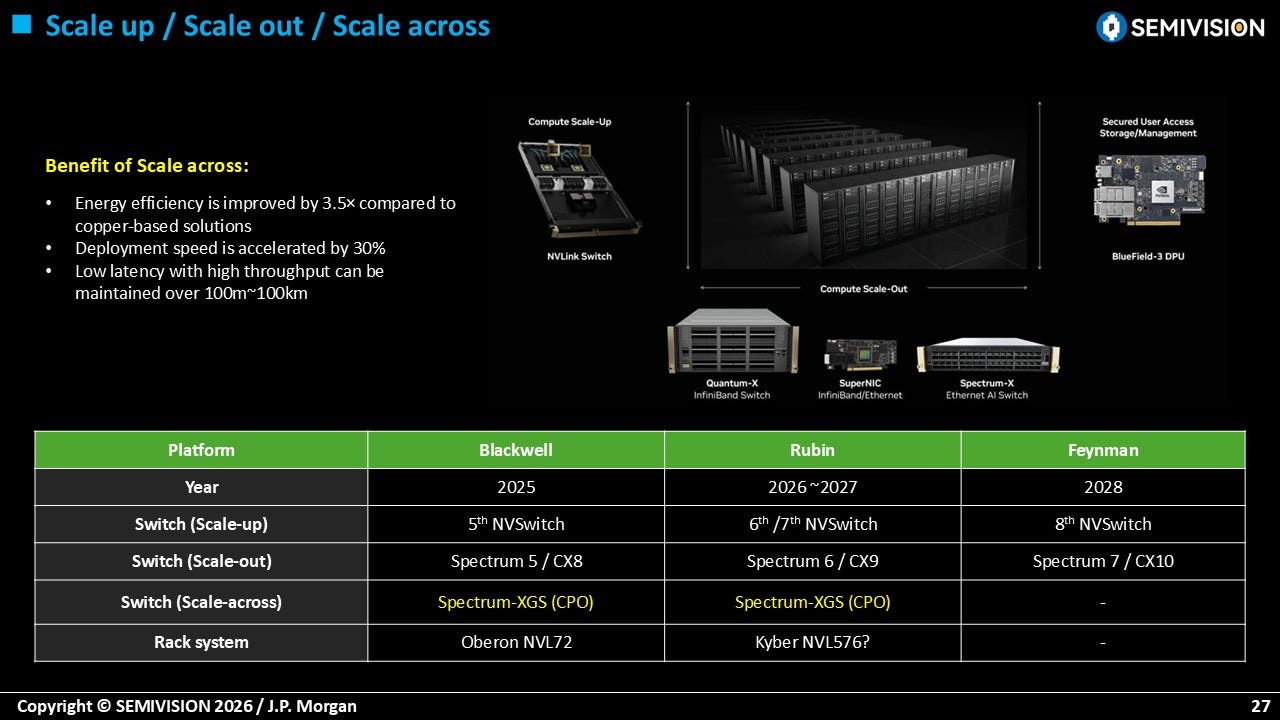
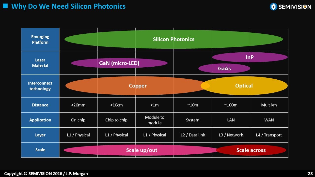
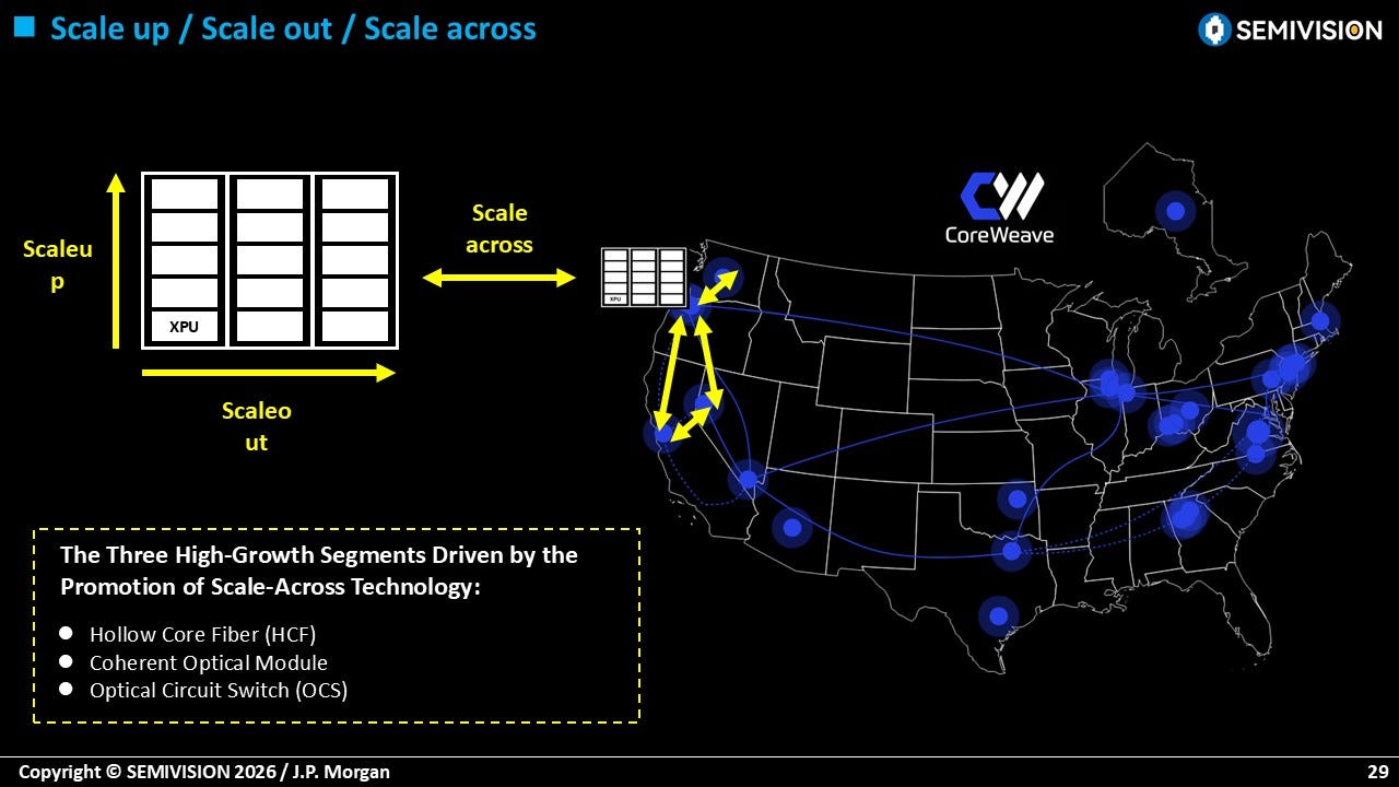



Conclusion and Outlook
Optical interconnects are gradually transitioning from laboratory research to large-scale commercial deployment, becoming an essential foundation for future AI and high-performance computing (HPC) systems. Through advanced packaging technologies such as CoWoS, SoIC, and COUPE, and by integrating photonic integrated circuits (PIC) and electronic integrated circuits (EIC) via hybrid bonding into a unified optical engine, TSMC has established a critical foundation for package-level optical interconnects.
Meanwhile, the 3D silicon photonics architecture presented by NVIDIA at ISSCC 2026 demonstrates that compute vendors are actively adopting new technologies—such as DWDM micro-ring resonators and forward clock architectures—to overcome bandwidth and latency bottlenecks.
At the same time, companies including Lightmatter, Celestial AI, Ayar Labs, and Ranovus are advancing optical engine technologies along different paths. These range from 1.6 Tb/s pluggable modules, to 6.4 Tb/s switch-class optical engines, and ultimately toward 12.8 Tb/s or higher CPO and optical I/O architectures, shaping both the competitive and collaborative landscape of the industry.
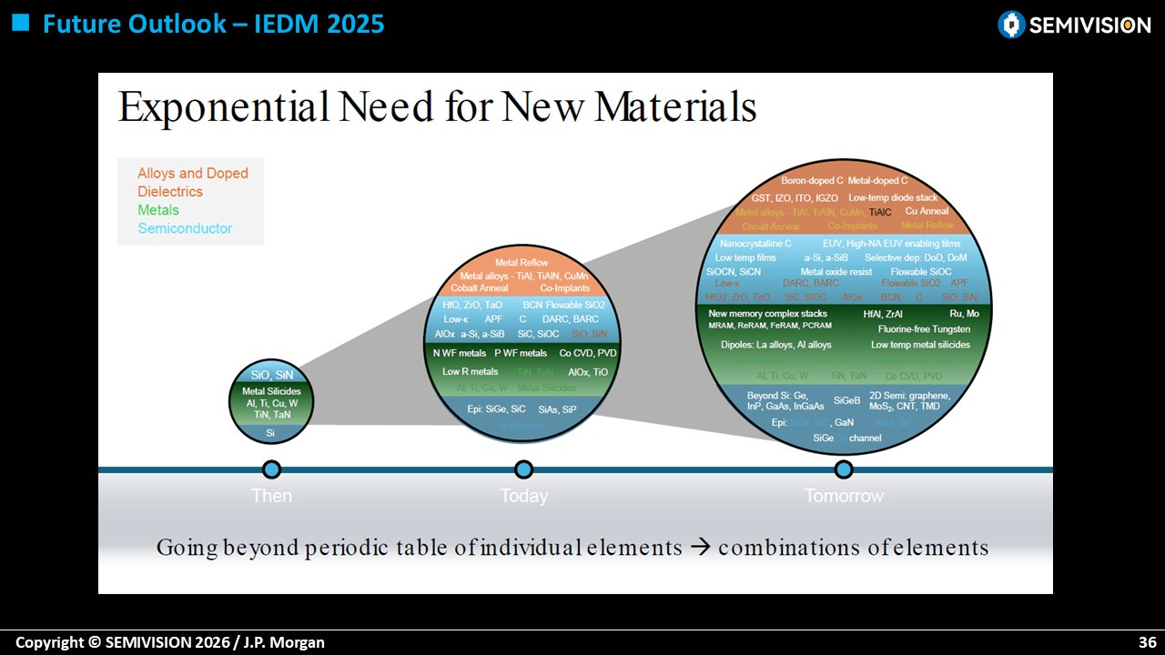
However, materials engineering and high-volume testing remain major challenges. Bonding materials between fiber array units (FAUs) and optical engines must balance both mechanical reliability and optical performance. Emerging material platforms—including III–V heterogeneous integration, 2D materials, and thin-film lithium niobate (TFLN)—are opening new possibilities for next-generation photonic devices.
At the same time, standardized optical probes, fiber connectors, and instrument calibration procedures will be critical for enabling high-throughput manufacturing and ensuring consistent product quality.
Looking ahead, the roadmap for optical interconnect technologies will involve comprehensive innovation across advanced packaging, silicon photonic circuits, materials science, and system architecture. From near-packaged optics (NPO) to co-packaged optics (CPO), and ultimately to fully integrating optical I/O directly into processor cores, this technological trajectory represents a new computing foundation for the post-Moore era.
As industry collaboration deepens and capital investment accelerates, optical interconnects are poised to become a key enabling technology for scaling AI training and inference infrastructure in the years ahead.

3月10日


PreviousNext
TopLatestDiscussions








See all